-
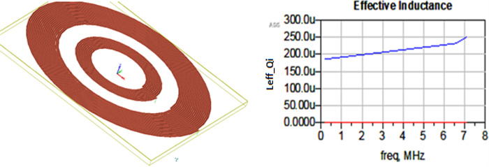
Figure 1.
The 3D EM modeling of the proposed concentric dual-band inductors.
-
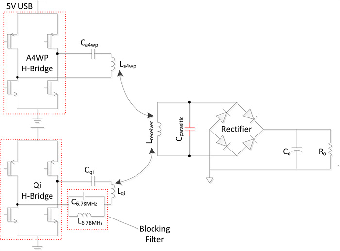
Figure 2.
Combined wireless power transfer system block diagram with blocking filter.
-
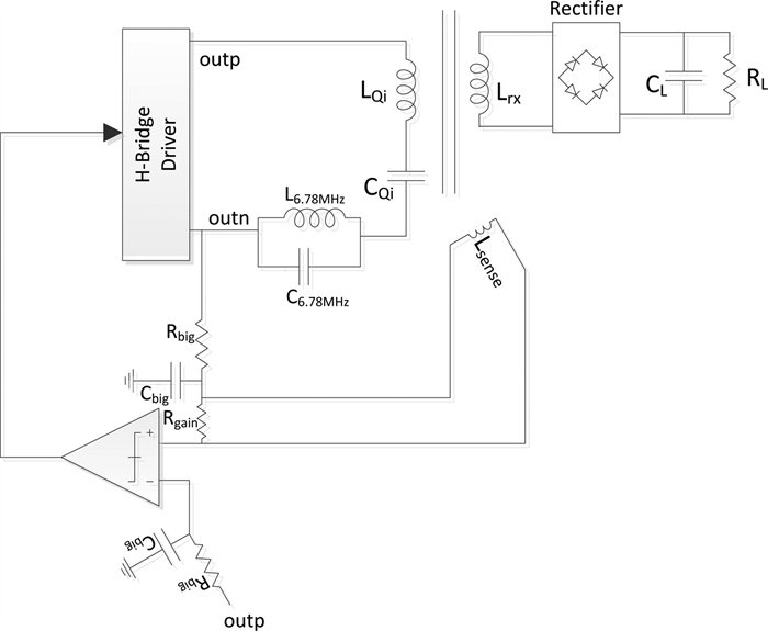
Figure 3.
Qi sub-system analog automatic-tracking resonance lock loop.
-
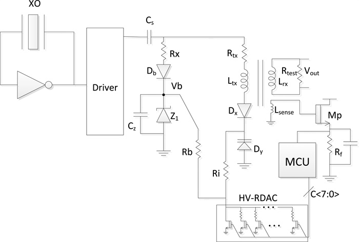
Figure 4.
High-speed A4WP sub-system resonance lock loop.
-
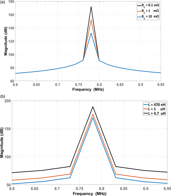
Figure 5.
(a) The bode diagram of Q factor of parallel LC filter by varying internal resistance of the inductor. (b) The bode diagram of Q factor of parallel LC filter by varying inductance value and capacitance value according to the resonance condition at 6.78 MHz.
-
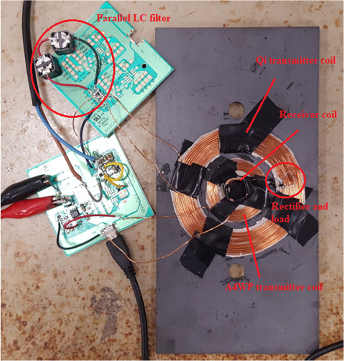
Figure 6.
Experimental prototype of the proposed combo system on a ferrite shield.
-
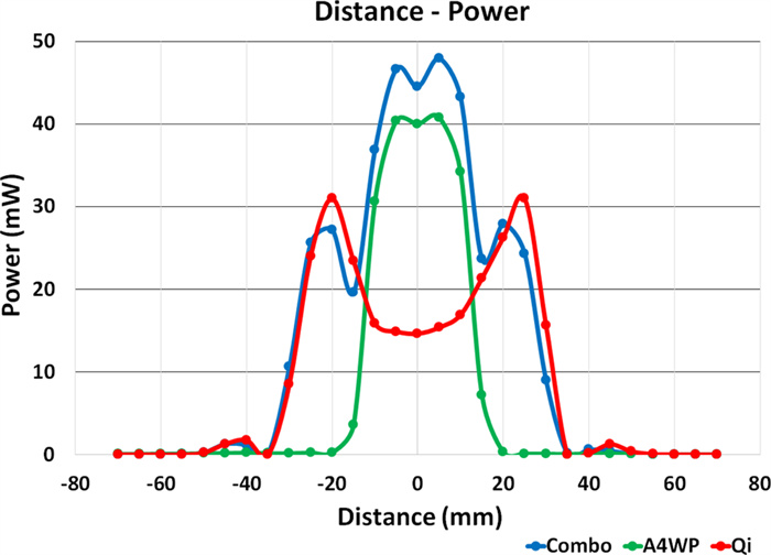
Figure 7.
The measured total RX power with respect to the position of receiver coil for all three types of transmitters.
-
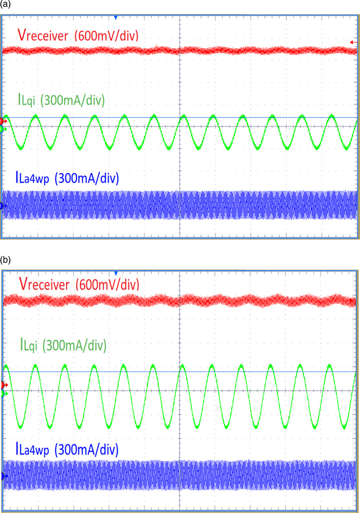
Figure 8.
(a) The measured output voltage and transmitter coil currents without parallel LC resonant filter. (b) With the blocking resonant filter in place.
-
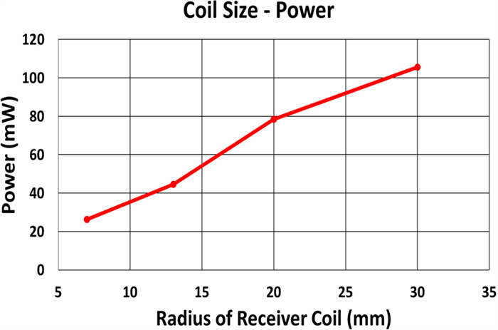
Figure 9.
Measurement results for output power versus 30-turn fixed coil radius.
-
Symbol Parameter values Ca4wp 76 pF La4wp 7.6 μH Cqi 7 nF Lqi 68 μH C6.78 MHz 95 pF L6.78 MHz 4.7 μH ESRL6.78 MHz 3 mOhm Table 1.
Optimized component values for the proposed combo system
-
Table 2.
Performance comparison with respect to various other studies in the literature
Figures
(9)
Tables
(2)