-
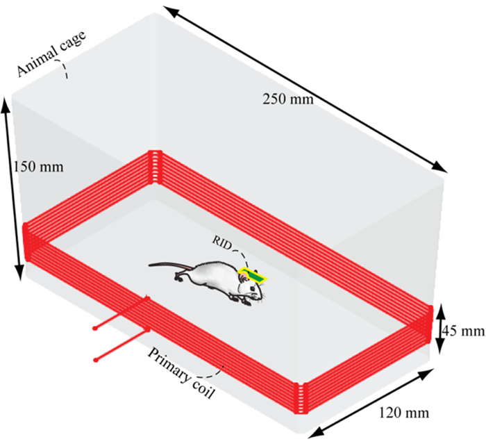
Figure 1.
WPT concept for a mouse, with primary coil wrapped around a small mouse housing cage.
-
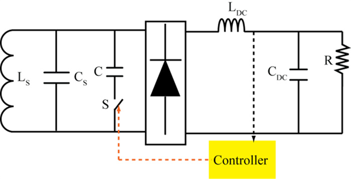
Figure 2.
Schematic of the DTD technique.
-
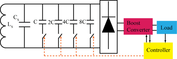
Figure 3.
Schematic using relay to tune the secondary circuit.
-
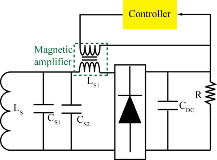
Figure 4.
Using magnetic amplifier in the secondary circuit.
-
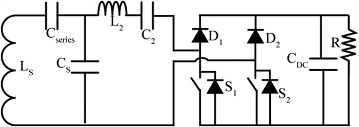
Figure 5.
Using fast switching in the secondary circuit.
-
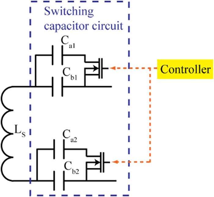
Figure 6.
Designed switching capacitors of [26].
-
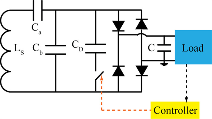
Figure 7.
Controlling open circuit impedance of the secondary circuit.
-
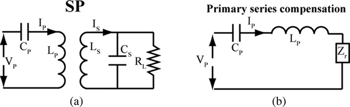
Figure 8.
SP topology of primary and secondary coils: (a) SP topology and (b) primary series compensation.
-
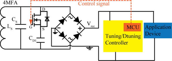
Figure 9.
Initial switching capacitor technique (non-working).
-
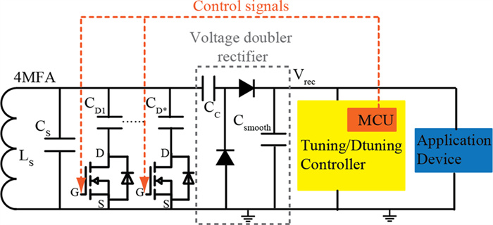
Figure 10.
Switching capacitor technique using a voltage doubler rectifier, whereby the source of the MOSFET is grounded on a common ground.
-
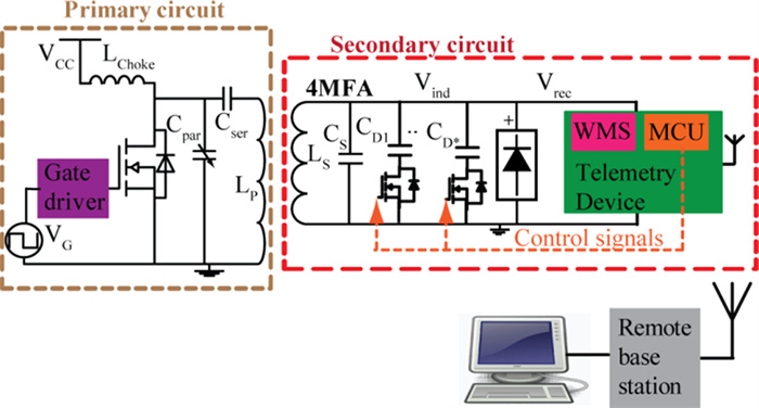
Figure 11.
Block diagram of our CTD LCWPT system.
-
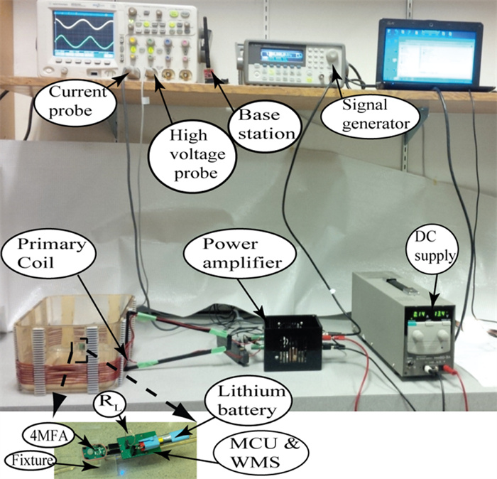
Figure 12.
Experimental setup of our controllable LCWPT system.
-
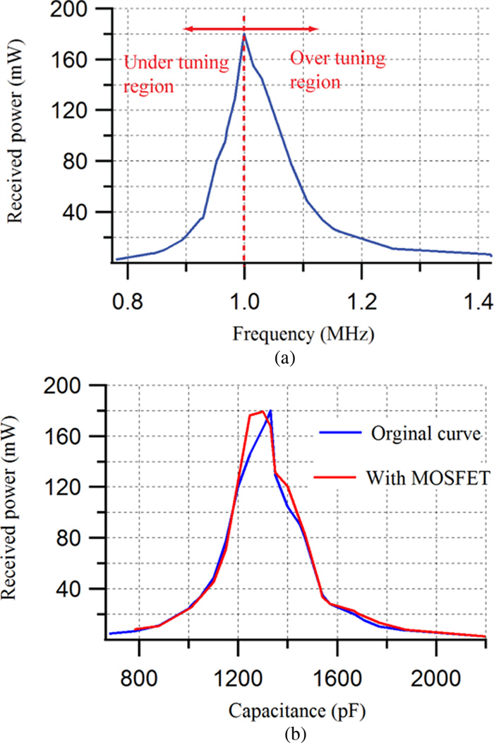
Figure 13.
Received power versus frequency/capacitance: (a) power versus frequency and (b) power versus capacitance with and without MOSFET.
-
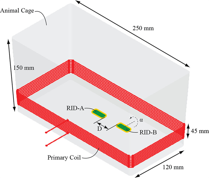
Figure 14.
WPT using multiple rodents in the same primary coil.
-
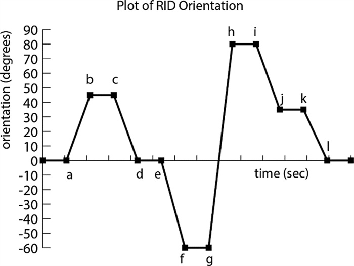
Figure 15.
Plot of RID orientation with respect to time, to simulate angles of rat's head.
-
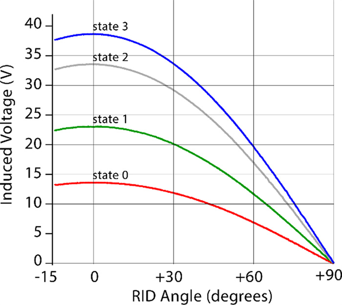
Figure 16.
Four operational states of RID showing Vrec versus orientation.
-
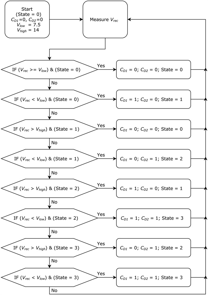
Figure 17.
Flow chart of control code for the CTD algorithm.
-
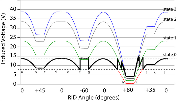
Figure 18.
Performance of CTD system switching between four states of the RID, showing Vrec versus orientation.
-
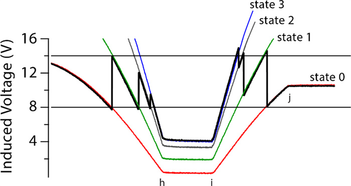
Figure 19.
Close-up of CTD system switching between four states in vicinity of segments h–i.
-
Configuration AWG RP (kΩ) Q L (μH) Primary coil (LP) 22 49.5 165 38.5 Secondary coil (LS) 44 8.2 55 19.3 Table 1.
Parameters of the primary and the secondary coils
-
RID-B at 0° RID-B at 30° Dist. D (cm) RID-A Vrec (V) P (mW) RID-A Vrec (V) P (mW) 0 40.9 167 41.6 173 1 41.2 170 41.9 176 2 41.8 175 42.3 179 3 42.1 177 42.4 180 4 42.3 179 42.4 180 5 42.4 180 42.4 180 6 42.4 180 42.4 180 Table 2.
Measurements of Vrec and received power for fixed RID-A, for orientations 0 and 30° of RID-B
-
RID-B at 60° RID-B at 90° Dist. D (cm) RID-A Vrec (V) P (mW) RID-A Vrec (V) P (mW) 0 41.9 176 42.2 178 1 42.2 178 42.4 180 2 42.4 180 42.4 180 3 42.4 180 42.4 180 4 42.4 180 42.4 180 5 42.4 180 42.4 180 6 42.4 180 42.4 180 Table 3.
Measurements of Vrec and received power for fixed RID-A, for orientations 60 and 90° of RID-B
-
RID state CS
320 pFCD1
100 pFCD2
150 pFVreca(V) Pa(mW) 3 – On On 38.7 150 1 – On Off 23.5 55 2 – Off On 33.5 112 0 – Off Off 13.5 18 aValues of Vrec and power correspond to 0° orientation of RID. Table 4.
Capacitor values for CTD switching experiment
Figures
(19)
Tables
(4)