-
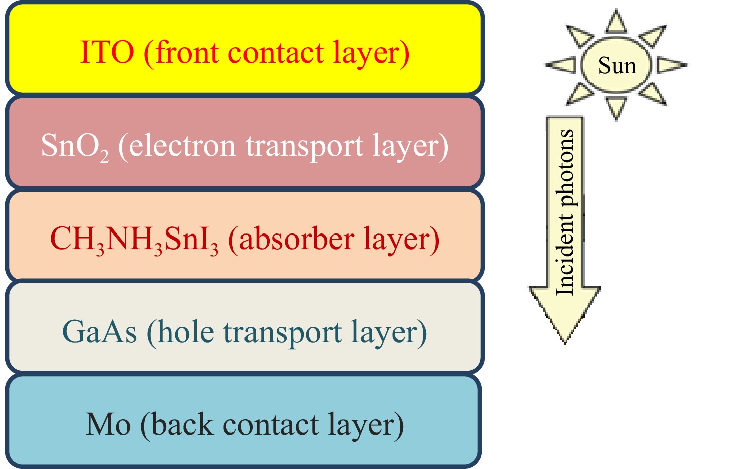
Figure 1.
Schematic structure of proposed device ITO/SnO2/CH3NH3SnI3/GaAs/Mo.
-
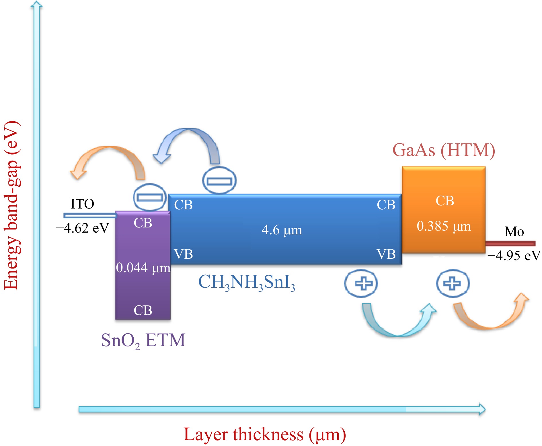
Figure 2.
Energy band-gap versus layer thickness of Perovskite solar cell.
-
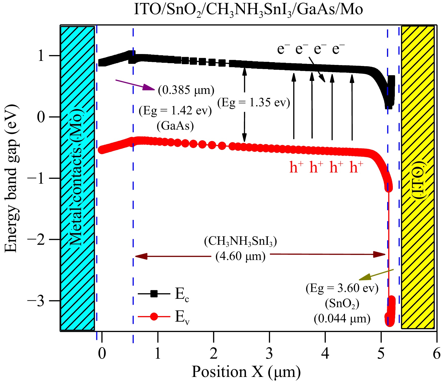
Figure 3.
Schematic diagram of valence and conduction band of ITO/SnO2/CH3NH3SnI3/GaAs/Mo solar cell.
-
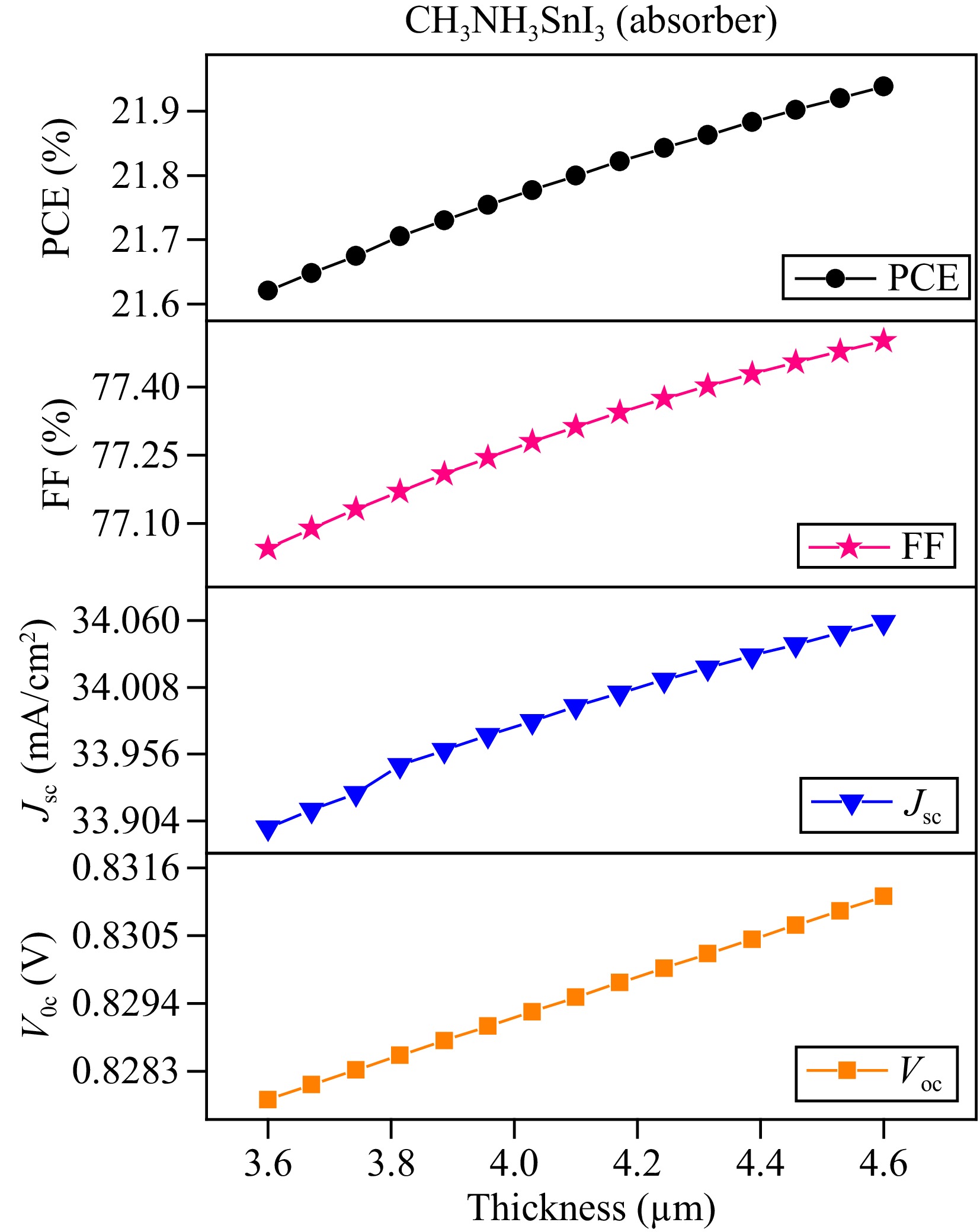
Figure 4.
Effect of absorber thickness on electrical parameters.
-
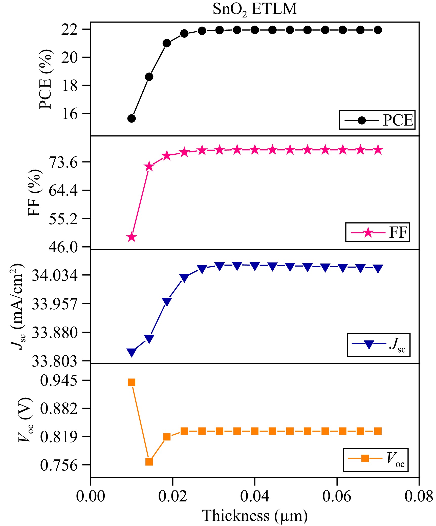
Figure 5.
Impact of ETL thickness variation on solar cell parameters.
-
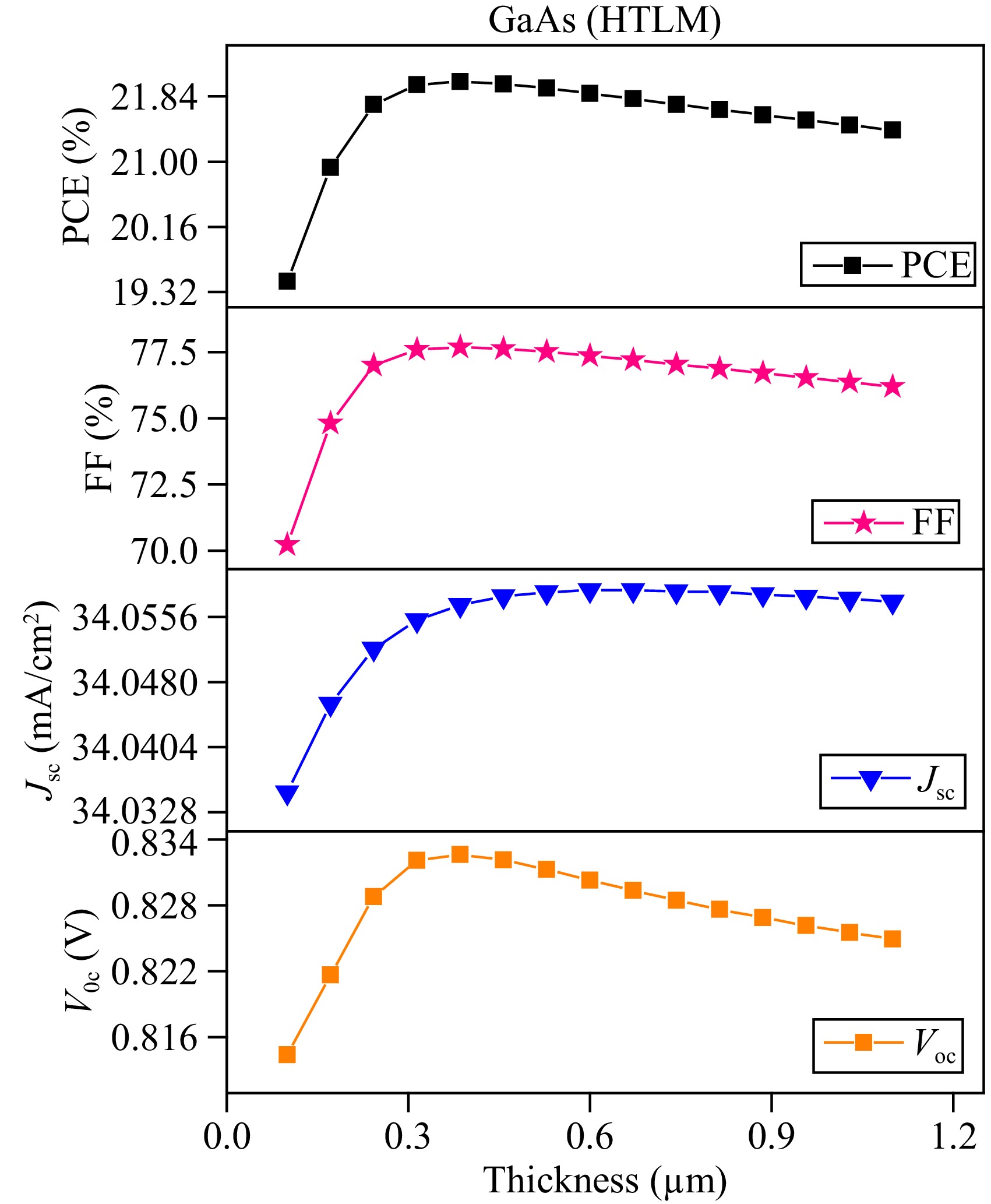
Figure 6.
Impact of HTL thickness variation on solar cell parameters.
-
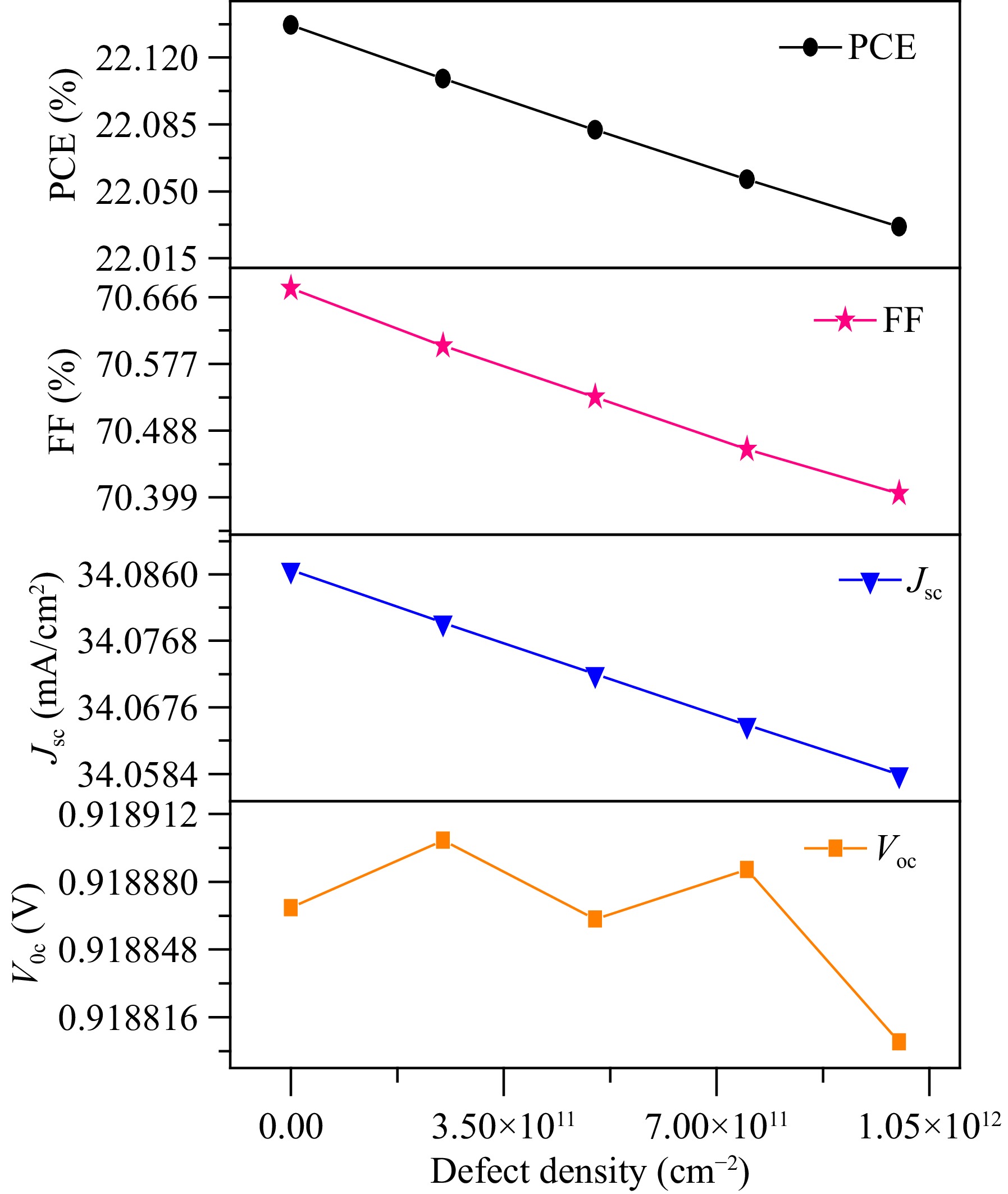
Figure 7.
Defect density versus electrical parameters.
-
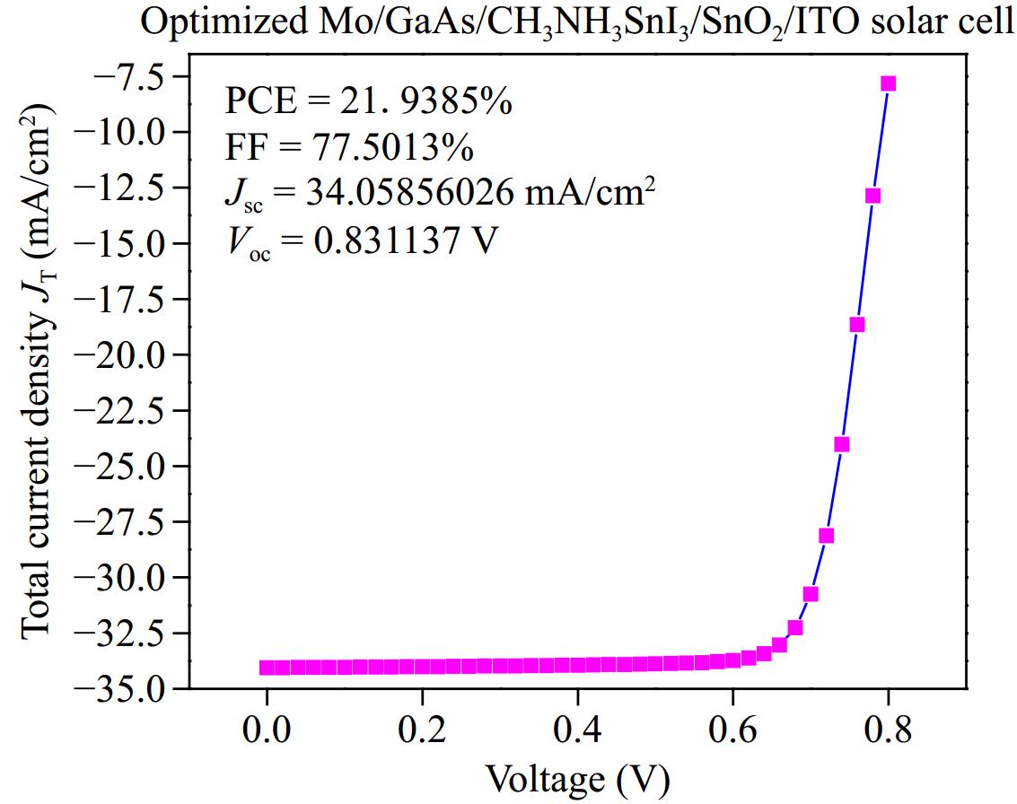
Figure 8.
Graph between current density and voltage.
-
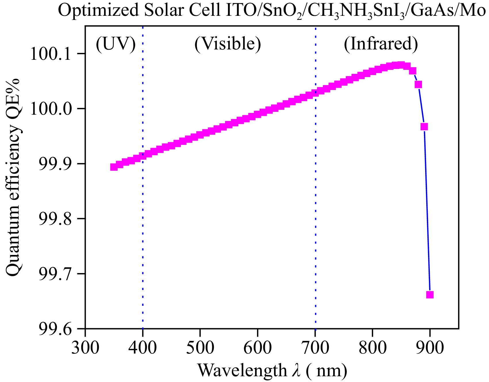
Figure 9.
Quantum efficiency vs wavelength.
-
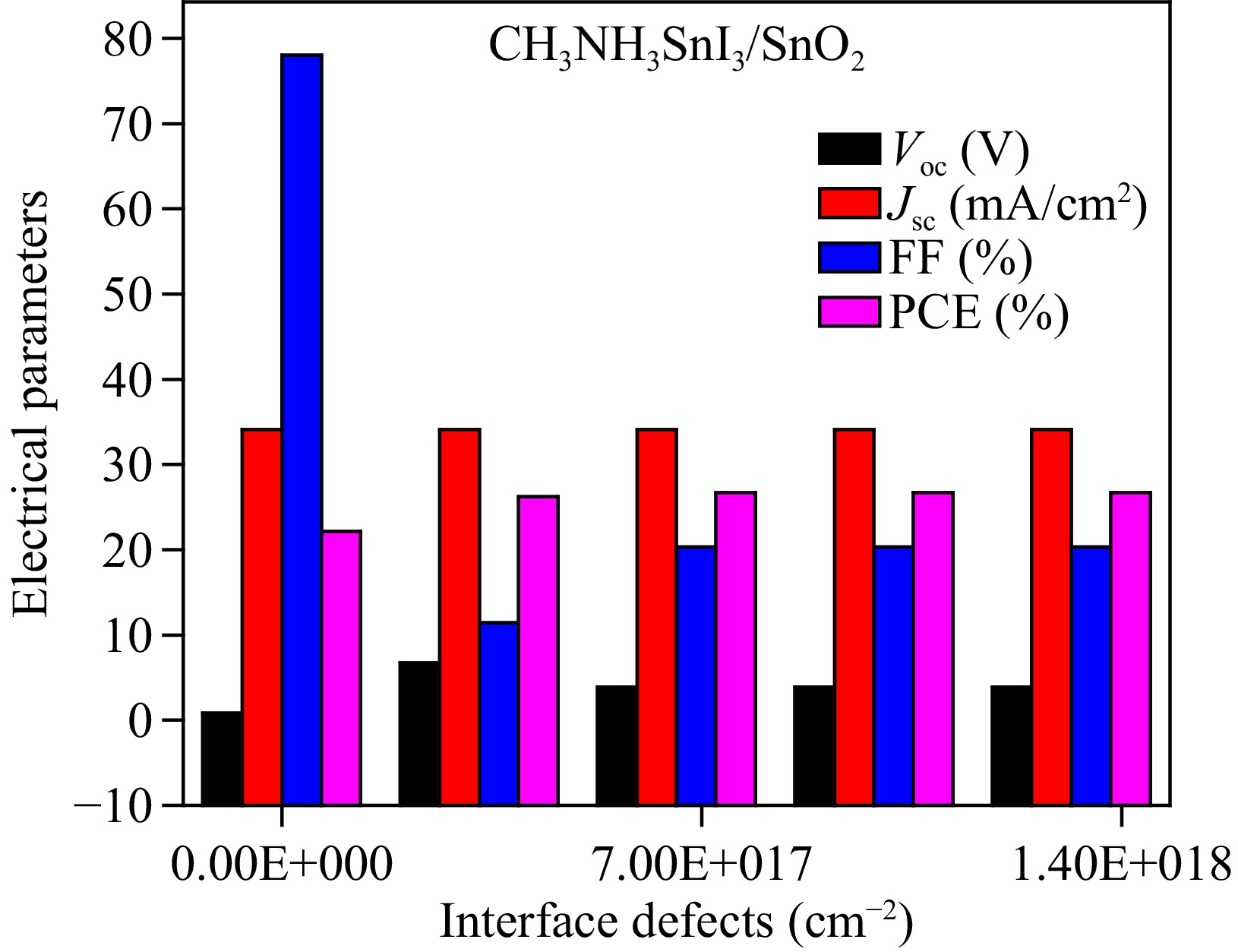
Figure 10.
Influence of interface defect density on photovoltaic parameters.
-
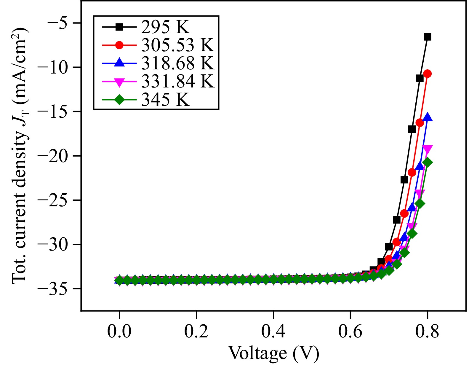
Figure 11.
Influence of temperature on Jsc and Voc.
-
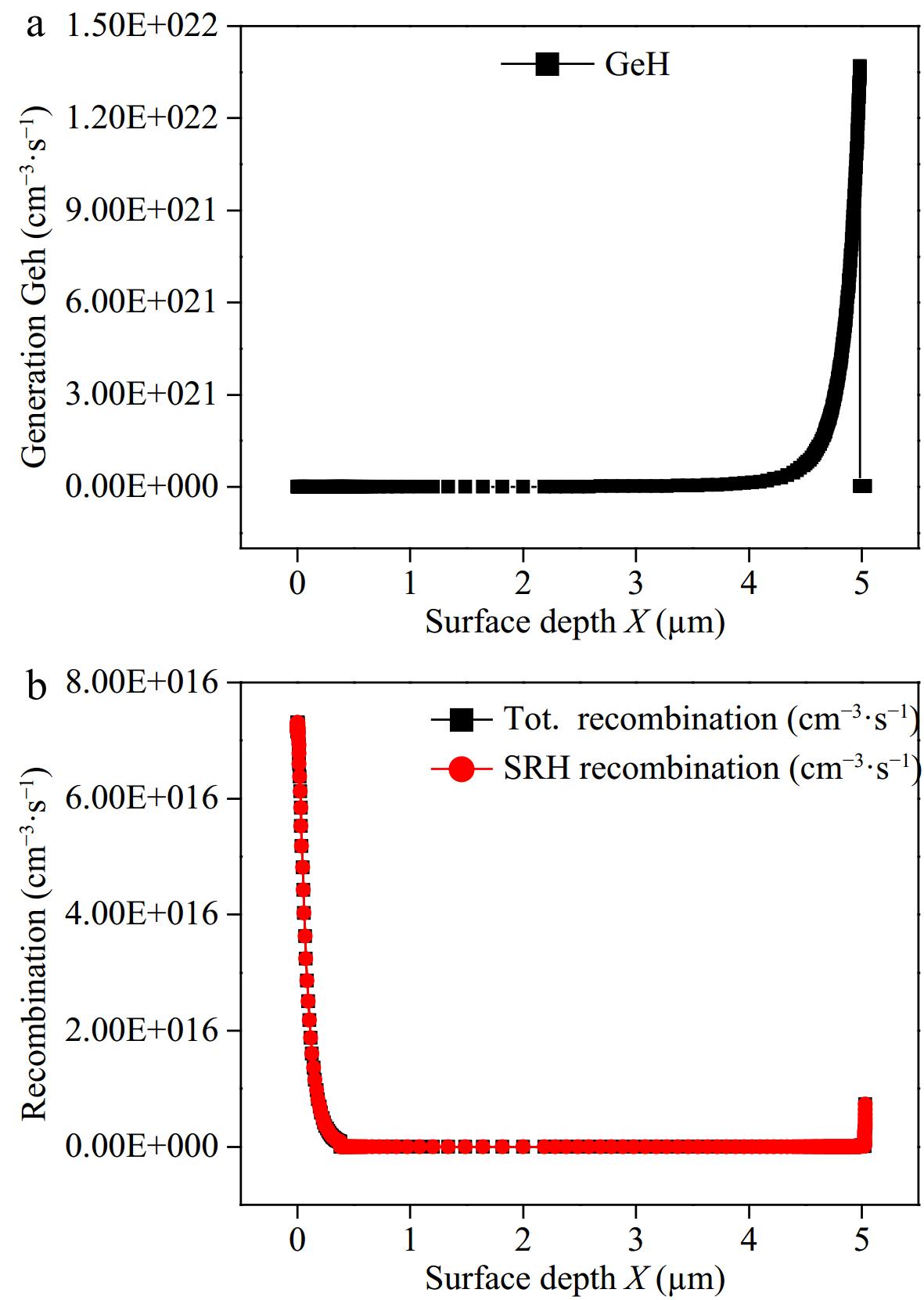
Figure 12.
(a) Variation in generation rate with surface depth of device. (b) Variation in recombination rate with surface depth of device.
-
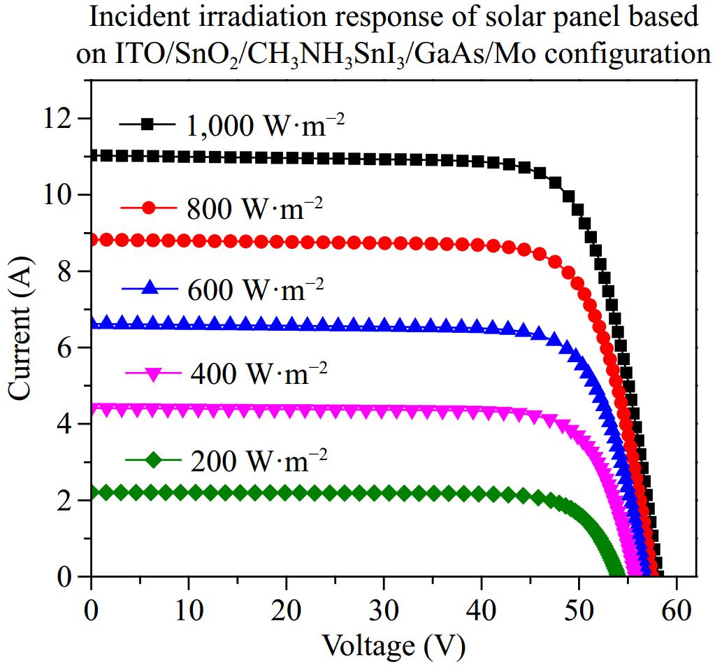
Figure 13.
Impact of light intensity on output characteristics of the solar panel.
-
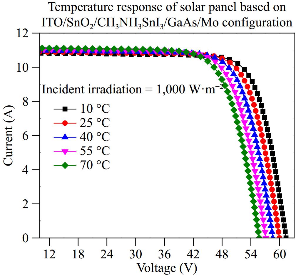
Figure 14.
Effect of temperature on I-V curve of the solar panel.
-
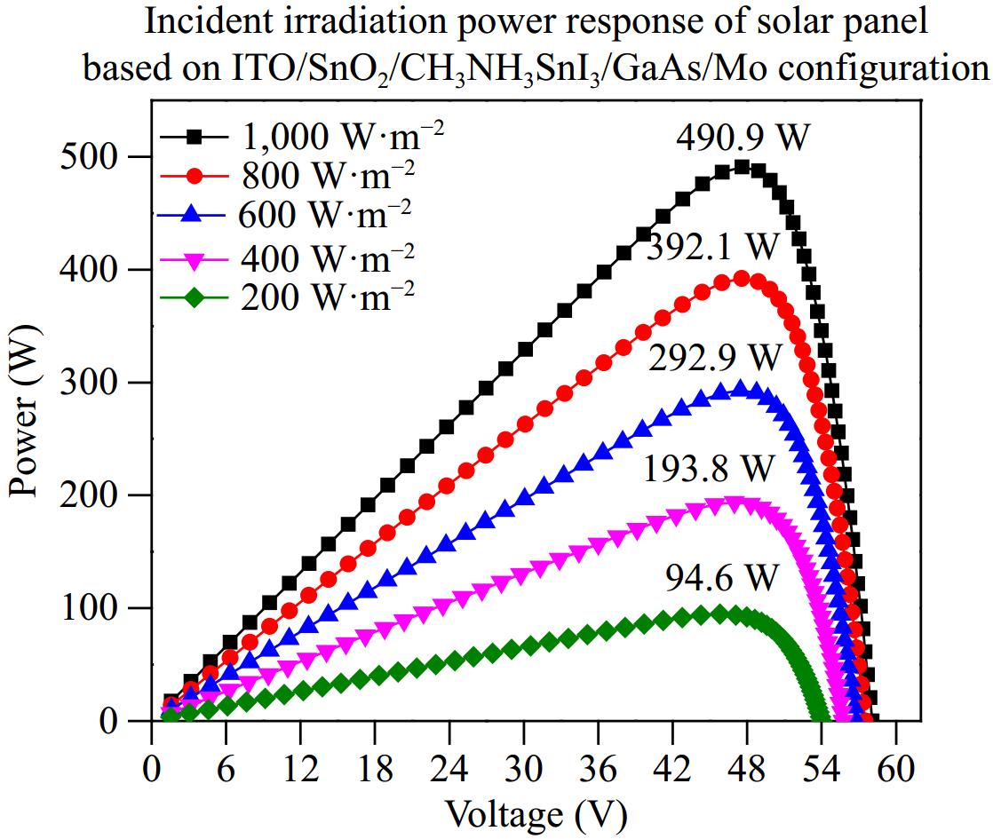
Figure 15.
Influence of light intensity on the output power of the solar panel.
-
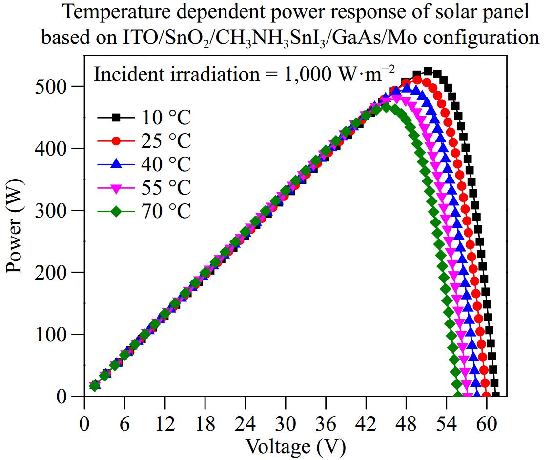
Figure 16.
Dependance of output power on the temperature of the solar panel.
-
Material parameters SnO2
(ETL)MASnI3
(absorber layer)GaAs
(HTL)X (μm) 0.044 Arbitrary 4.60 Arbitrary 0.385 Arbitrary Eg (eV) 3.60 1.35 1.42 χ (eV) 4.000 4.17 4.070 ε (relative) 9.000 6.500 12.900 Nc (cm−3) 2.200E+18 1.000E+18 2.200E+18 Nv (cm−3) 1.800E+19 1.000E+19 1.800E+19 Ve (cms−1) 1.000E+7 1.000E+7 1.00E+7 Vh (cms−1) 1.000E+7 1.000E+7 1.00E+7 μe (cm2V−1-s1) 1.000E+2 1.600E+0 8.500E+3 μh (cm2V−1-s1) 2.500E+1 1.600E+0 4.000E+2 ND (cm−3) 1.000E+18 0.0 0.0 NA (cm−3) 0.0 3.200E+15 1.000E+11 Nt (cm−3) 1.000E+15 − 1.000E+14 Nt (cm−3) 5.642E+15 − Table 1.
Material parameters of HTLs, absorber layer and ETL.
-
Material parameters CuI/CH3NH3SnI3
interfaceCuSCN/CH3NH3SnI3
interfaceCH3NH3SnI3/C60
interfaceDefect type Neutral Neutral Neutral Capture cross section for (n,p) (cm−2) 1 × 10⁻¹⁹ 1 × 10⁻¹⁹ 1 × 10⁻¹⁹ Energy distribution Single Single Single E- level w.r.t Ev (above Ev, Ev) 0.6 0.6 0.6 Total density (cm−3) 1 × 10¹³ 1 × 10¹³ 1 × 10¹³ Table 2.
Material parameters of HTLs/ CH3NH3SnI3 interface defects and CH3NH3SnI3/ C60 interface defects.
Figures
(16)
Tables
(2)