-
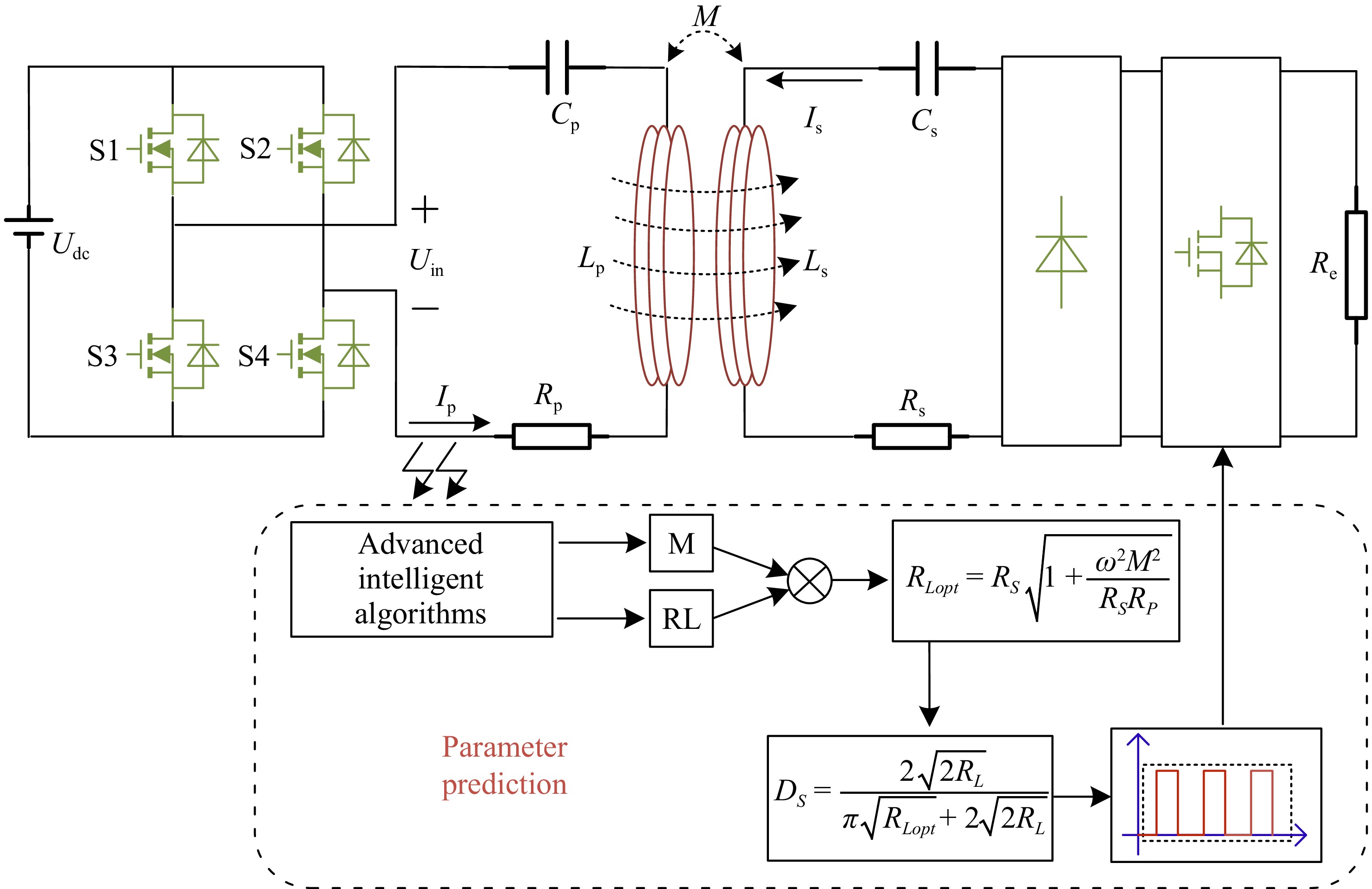
Figure 1.
SS type topology structure input by inverter.
-
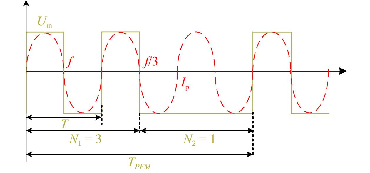
Figure 2.
PFM theoretical modulation waveform.
-
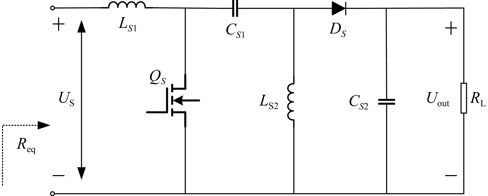
Figure 3.
Receiver added to the Sepic circuit.
-
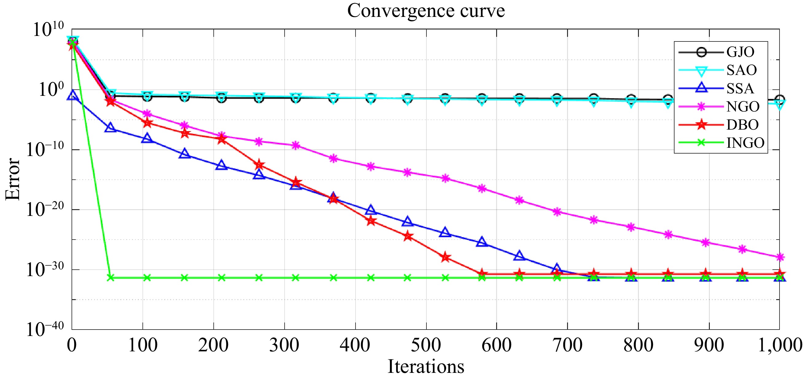
Figure 4.
Comparison of the performance of the optimization proposed in this paper with the remaining several optimizations.
-
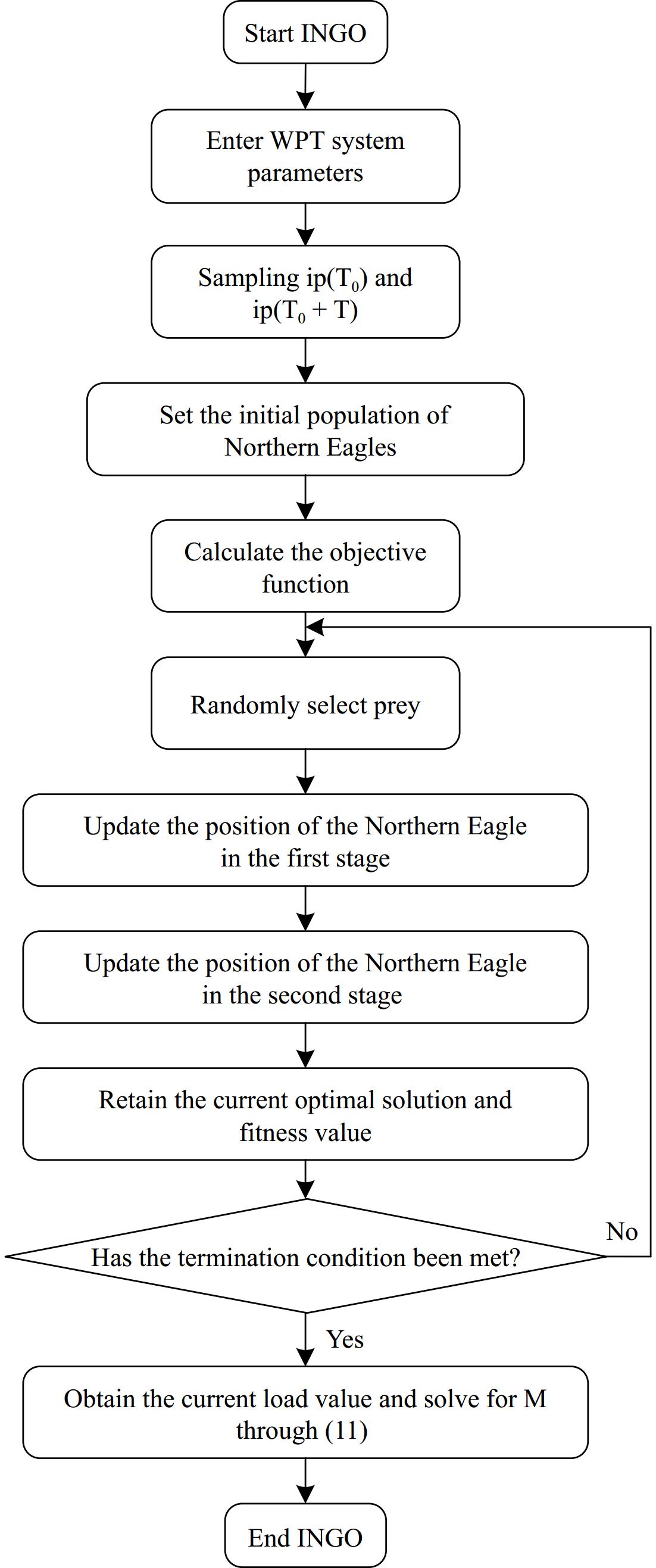
Figure 5.
INGO recognition flowchart.
-
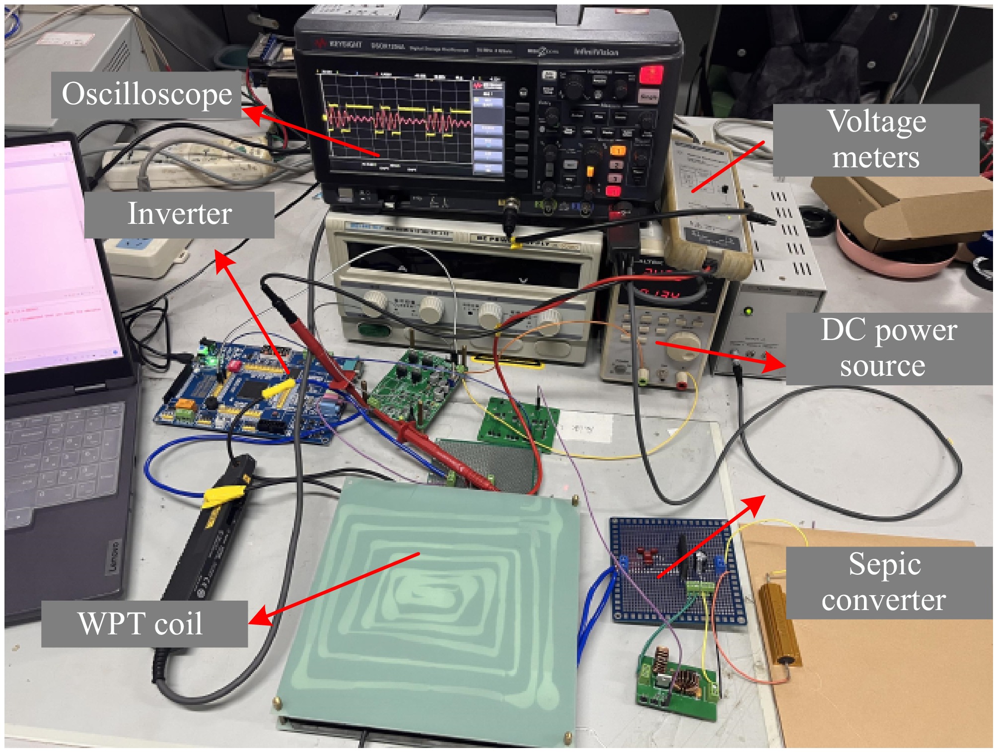
Figure 6.
Experimental model of the proposed WPT system.
-
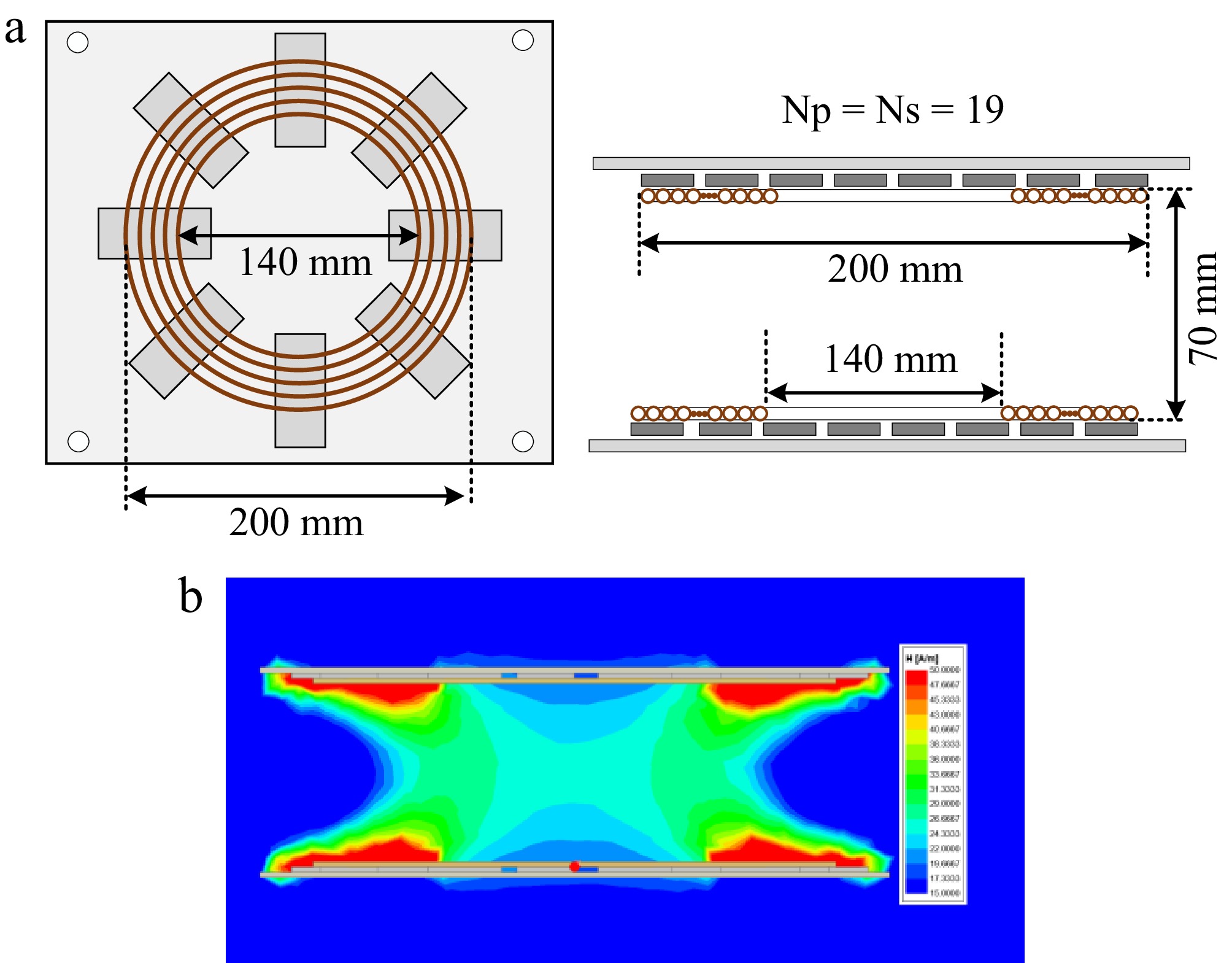
Figure 7.
(a) Transmitter and receiver side coil geometry. (b) Coil magnetic field distribution.
-
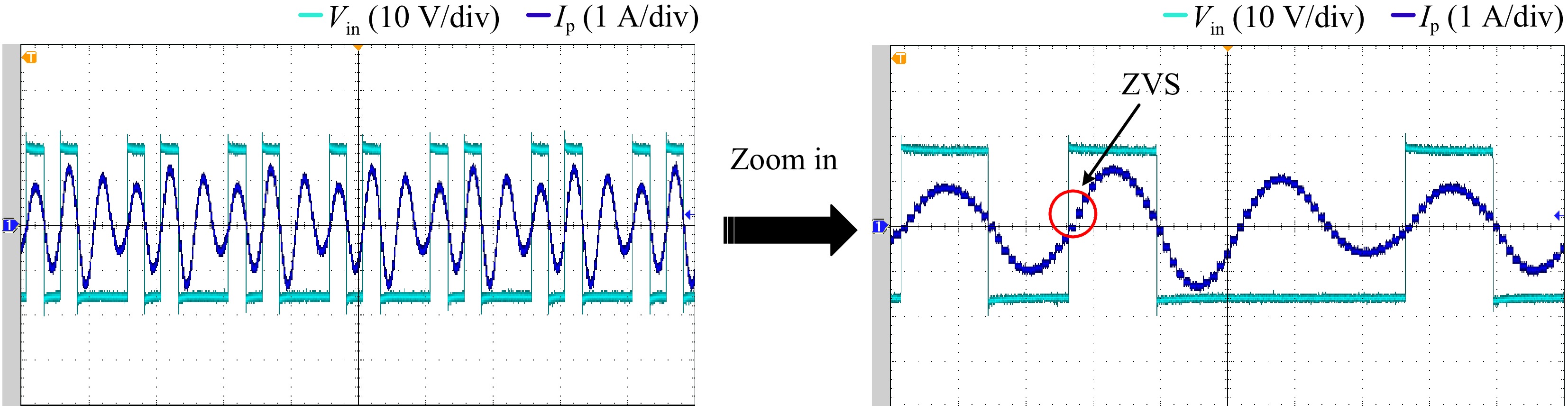
Figure 8.
Measured waveform of the PFM transmitter.
-
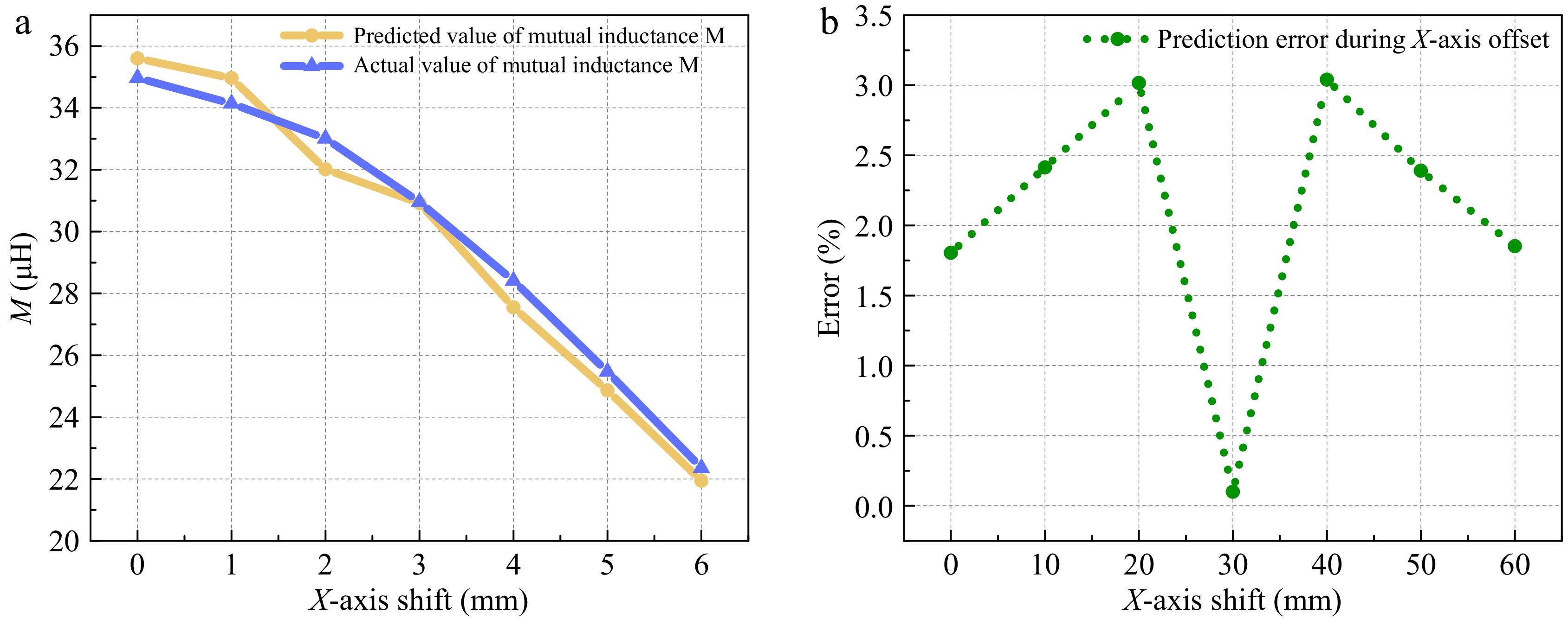
Figure 9.
Comparison between the actual value of mutual sensing and the recognition result at lateral offset. (a) Comparison of identified and actual values. (b) Error.
-
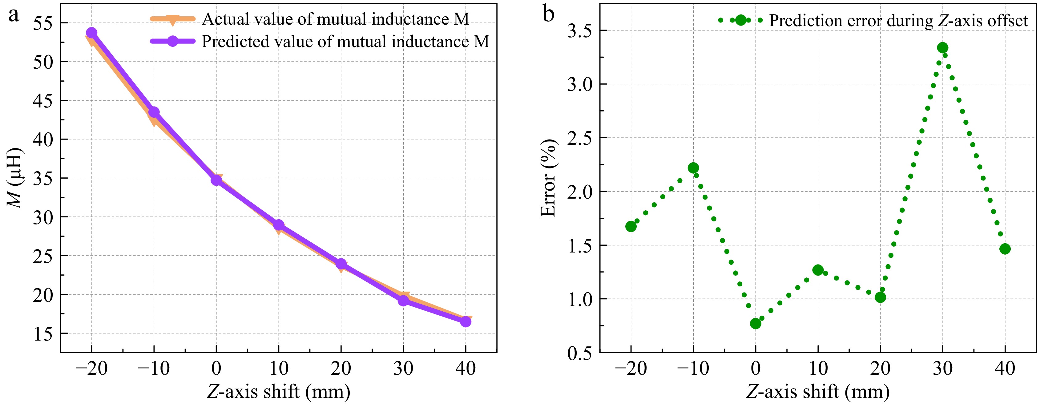
Figure 10.
Comparison between the actual value of mutual sensing and the recognition result at longitudinal offset. (a) Comparison of identified and actual values. (b) Error.
-
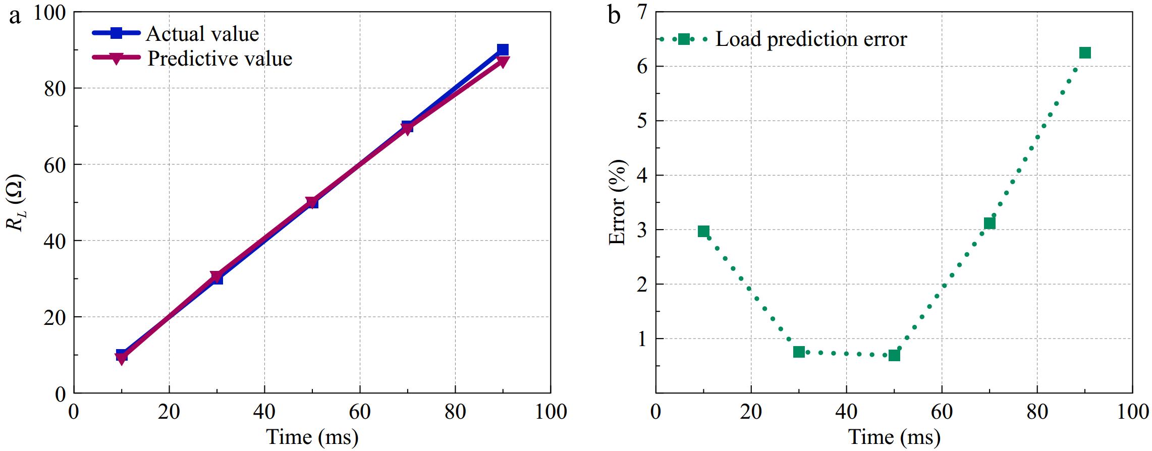
Figure 11.
Comparison of recognised values with actual values when the load changes (a) Comparison of identified and actual values. (b) Error.
-
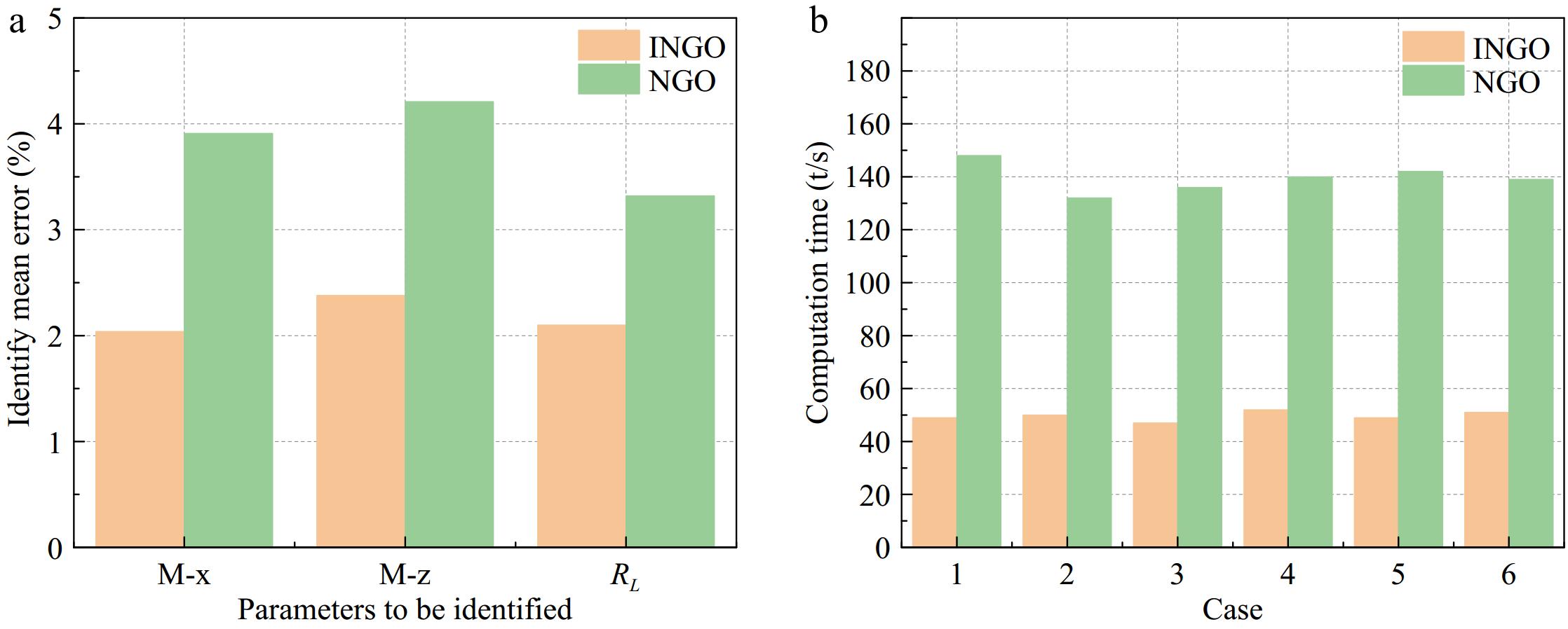
Figure 12.
Comparison of INGO and NGO algorithms. (a) Comparison of average error. (b) Comparison of computing time.
-
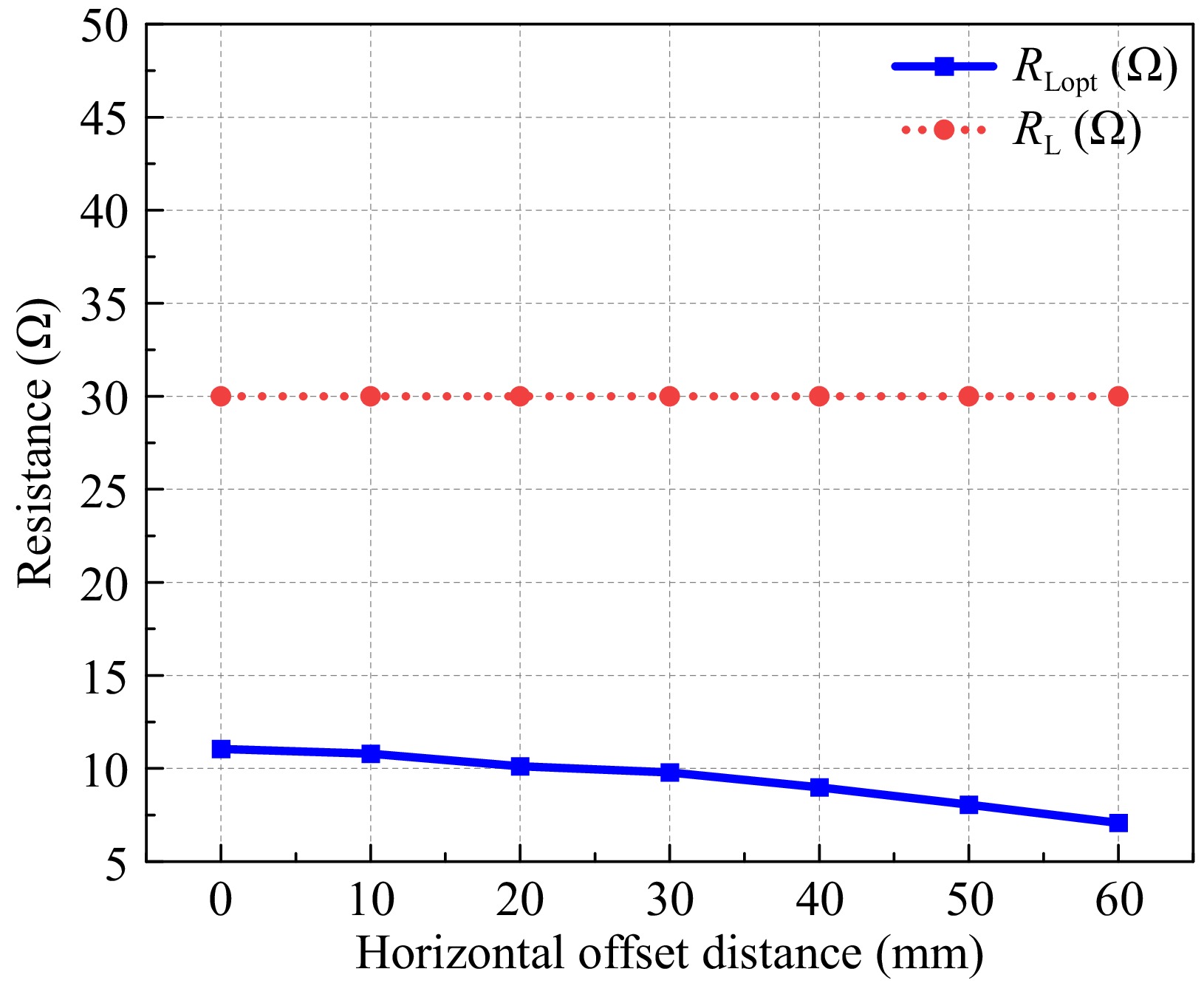
Figure 13.
Equivalent resistance calculated from recognised mutual inductance.
-
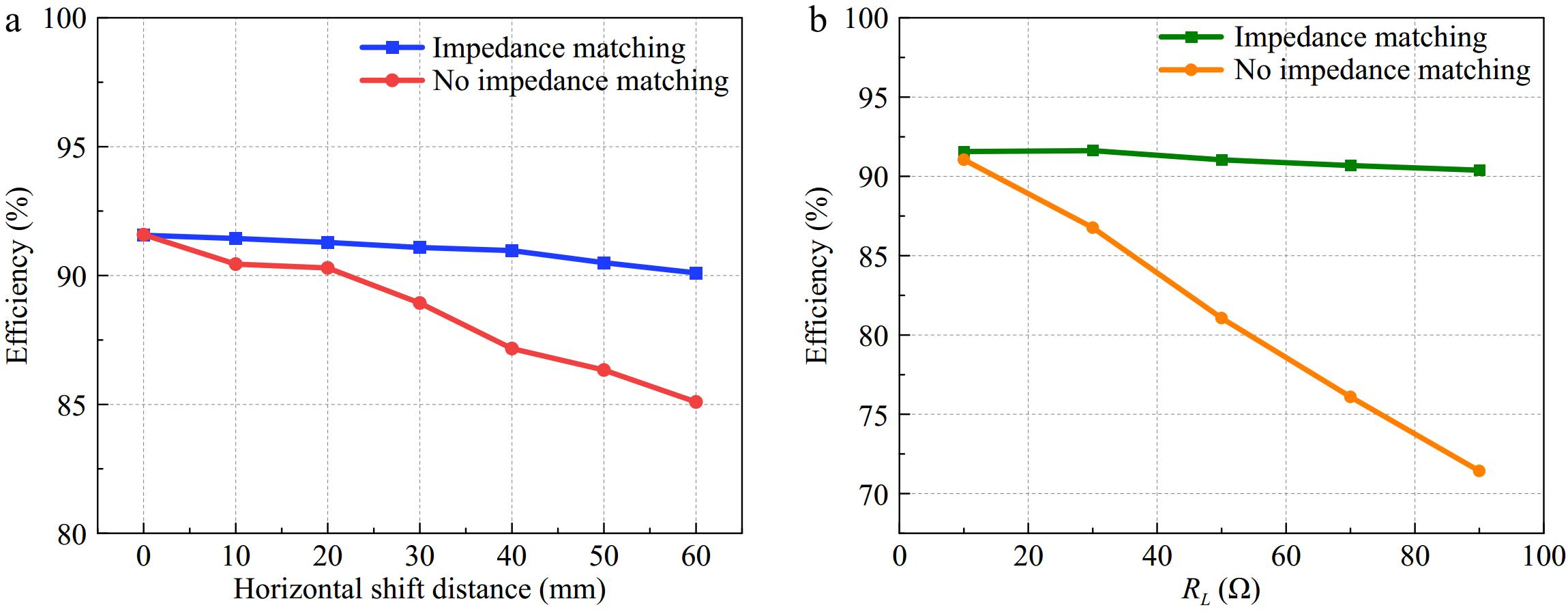
Figure 14.
Transmission efficiency with or without impedance matching applied (a) coil shift, (b) load variation.
-
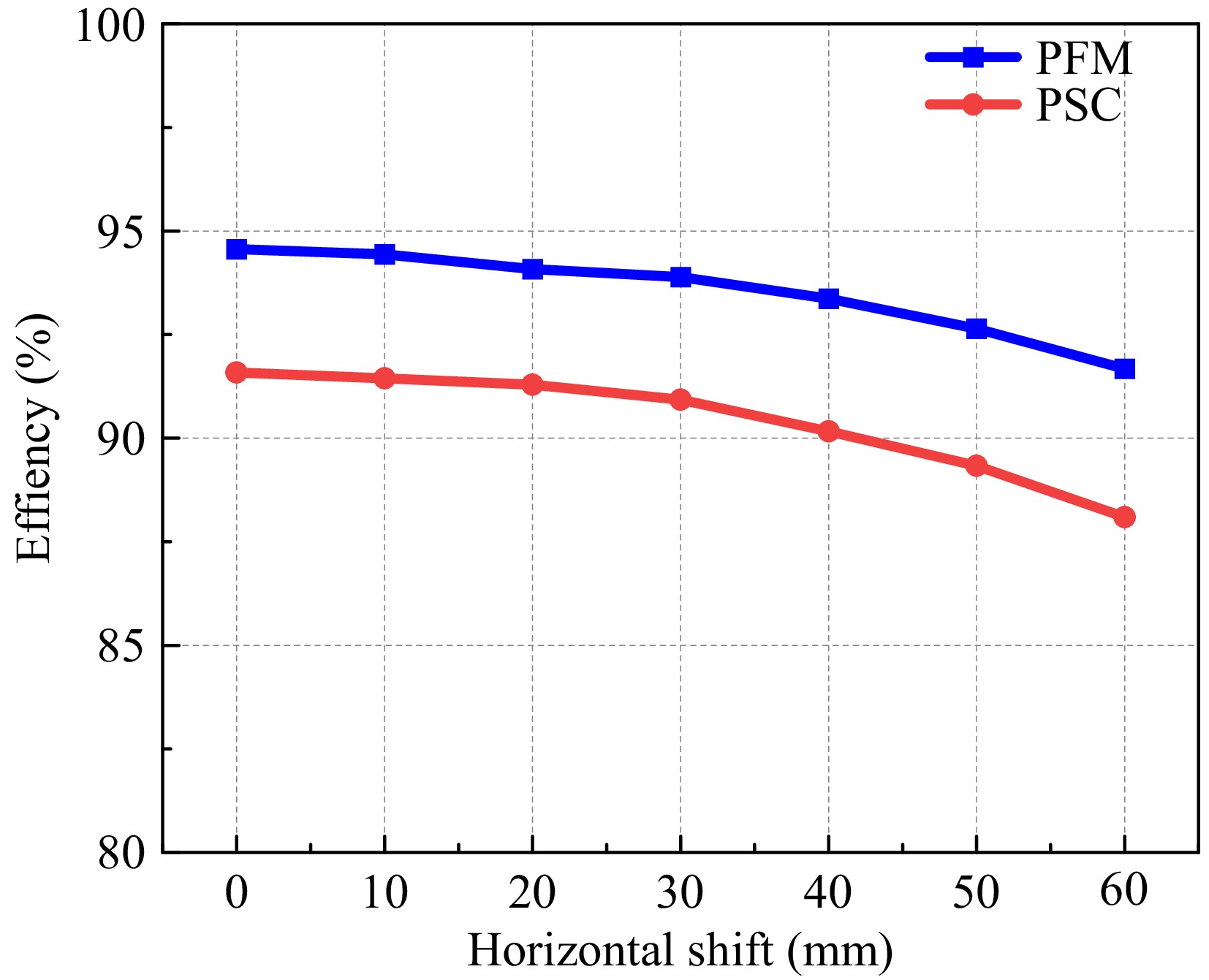
Figure 15.
Comparison of efficiency at different control strategies.
-
Characteristic Sepic Boost Buck-Boost Cuk Zeta The range of Req 0 ~ $ + \infty $ 0 ~ RL 0 ~ $ + \infty $ 0 ~ $ + \infty $ 0 ~ $ + \infty $ The polarity of US/Uo Same Same Reverse Reverse Reverse Conversion efficiency Higher higher medium medium medium Input current continuity Continuous Discontinuous Discontinuous Continuous Continuous Cost medium Lower medium higher higher Table 1.
Comparison of five basic DC-DC converters
-
Algorithm Avg. error (%) Iterations Computation time (t/s) INGO 1.5% 87 50 SAO 3.8% 50 30 SSA 1.5% 49 110 DBO 1.5% 581 80 GJO 3.8% 726 30 Table 2.
Comparison with other algorithms in parameter identification.
-
Items Value DC input voltage (Udc) 24 V Transmitter compensated capacitance (CP) 16.5 nF Transmitter coil inductance (LP) 152.87μH Receiver compensated capacitance (CS) 16.49 nF Receiver inductances (LS) 153.6 μH Sepic inductances (LS1) 34.6 μH Sepic inductances (LS2) 33.4 μH Sepic compensated capacitance (CS1) 47 μF Sepic output capacitance (CS2) 2,200 μF Fundamental switching frequency (f) 100 kHz Table 3.
Design parameters and specifications.
-
0ffset (cm) R (Ω) M-x (μH) 1 30 34.14 2 30 33.01 3 30 30.95 4 30 28.41 5 30 25.47 6 30 22.35 Table 4.
Identification parameter value of mutual inductance parameter change.
-
0ffset (cm) R (Ω) M-z (μH) −2 30 53.72 −1 30 43.49 1 30 28.95 2 30 23.93 3 30 19.17 4 30 16.47 Table 5.
Identification parameter value of mutual inductance parameter change.
-
Case R (Ω) M (μH) 1 10 34.97 2 30 34.97 3 50 34.97 4 70 34.97 5 90 34.97 Table 6.
Identification of parameter values for load parameter variations.
-
Table 7.
Compared with other identification methods.
Figures
(15)
Tables
(7)