-
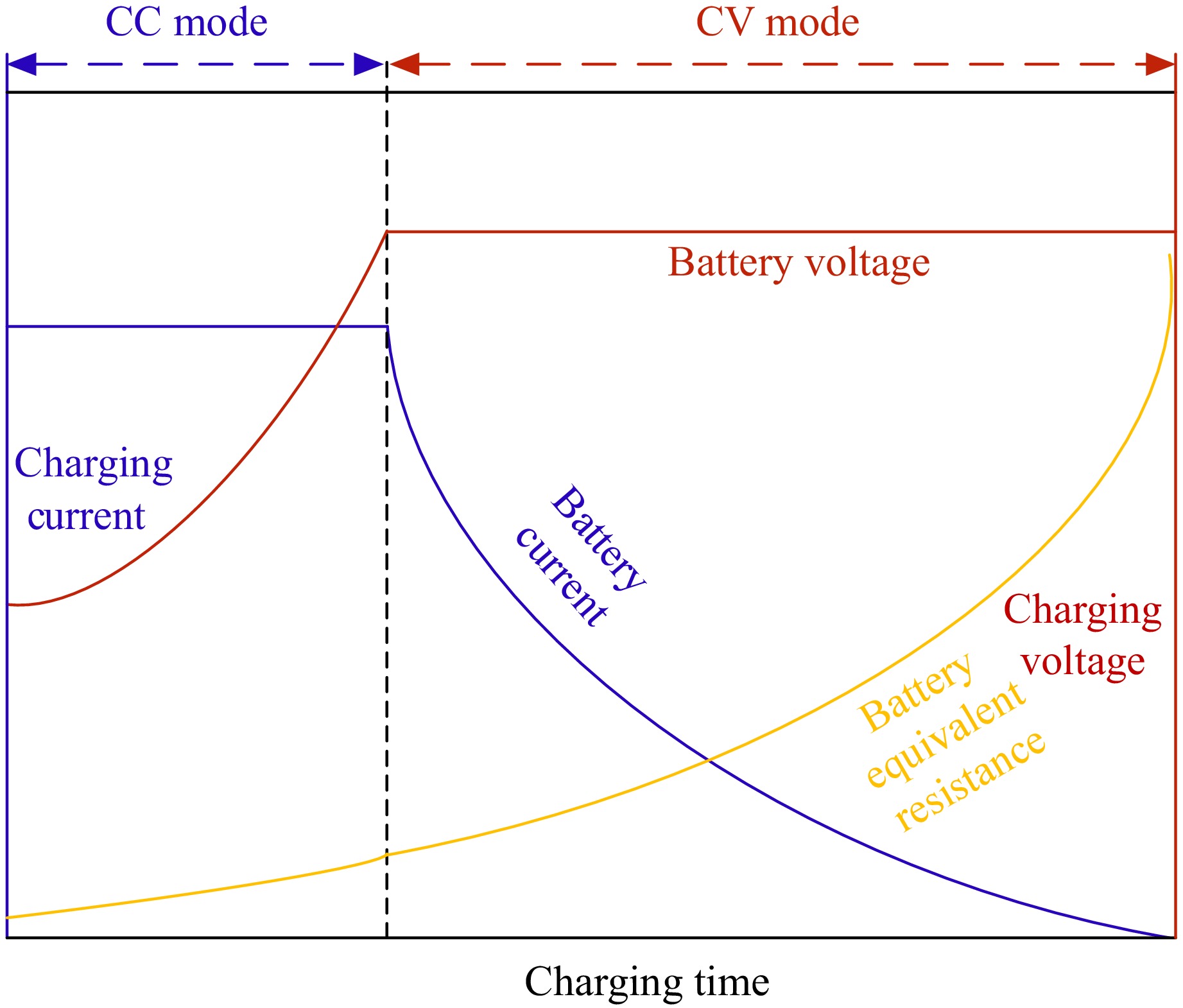
Figure 1.
Charging curve of a battery.
-
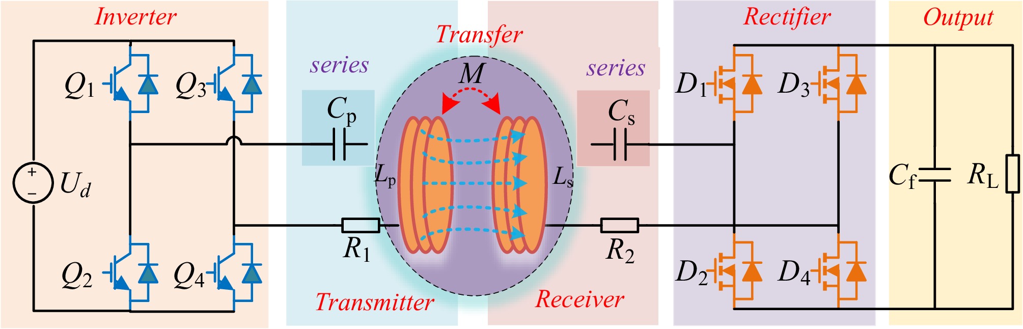
Figure 2.
WPT system architecture with S/S compensation structure.
-
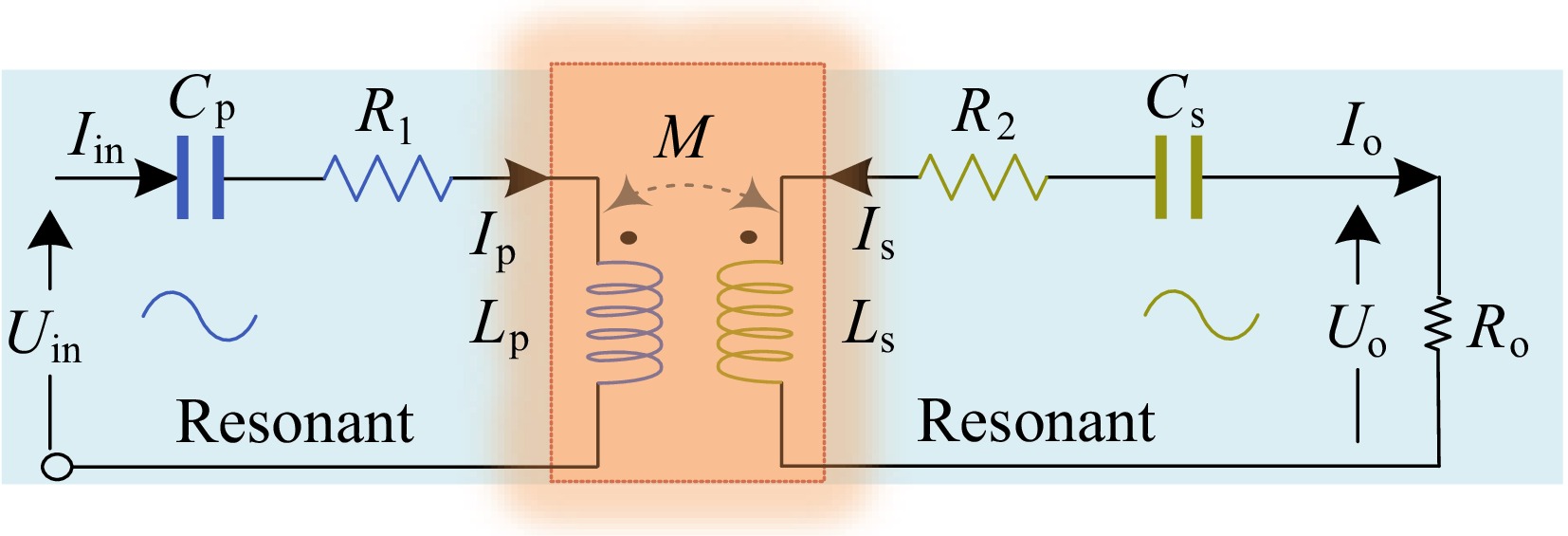
Figure 3.
Equivalent circuit diagram of the WPT system with S/S compensation structure.
-
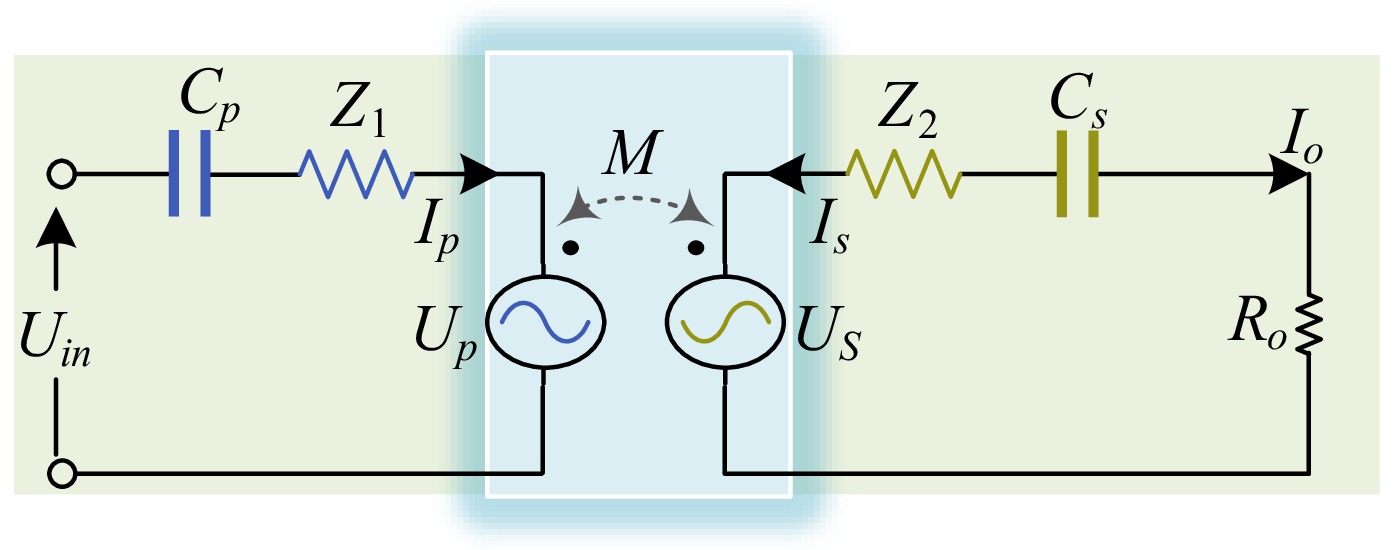
Figure 4.
Mutual inductance model of WPT system with S/S compensation structure.
-
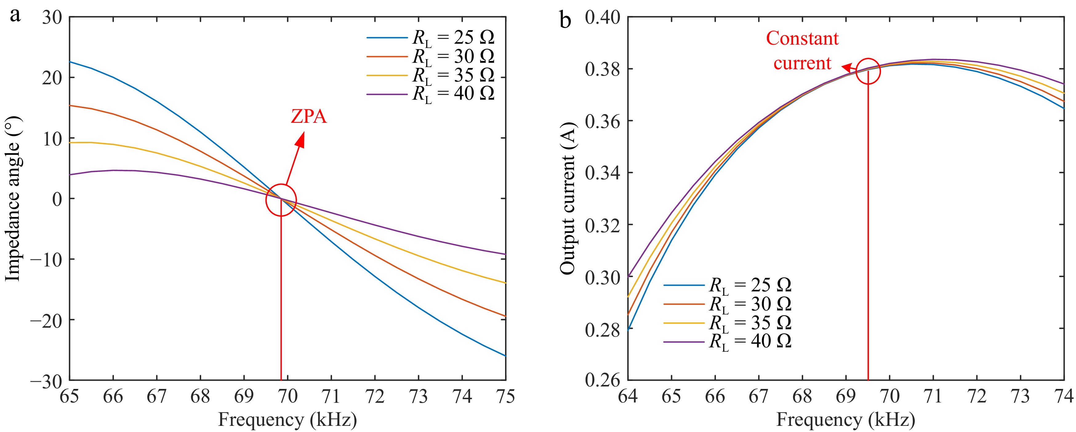
Figure 5.
Relationship between load resistance RL and output current and input impedance angle under different frequencies in CC mode. (a) Impedance angle under different loads for frequency change. (b) CC output characteristics.
-
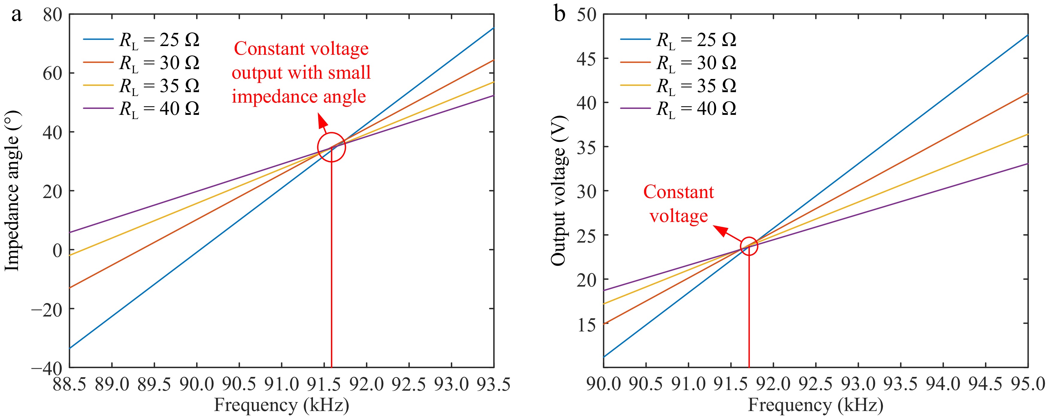
Figure 6.
Relationship between load resistance RL and output voltage and input impedance angle under different frequencies in CV mode. (a) Impedance angle under different loads for frequency change. (b) CV output characteristics.
-
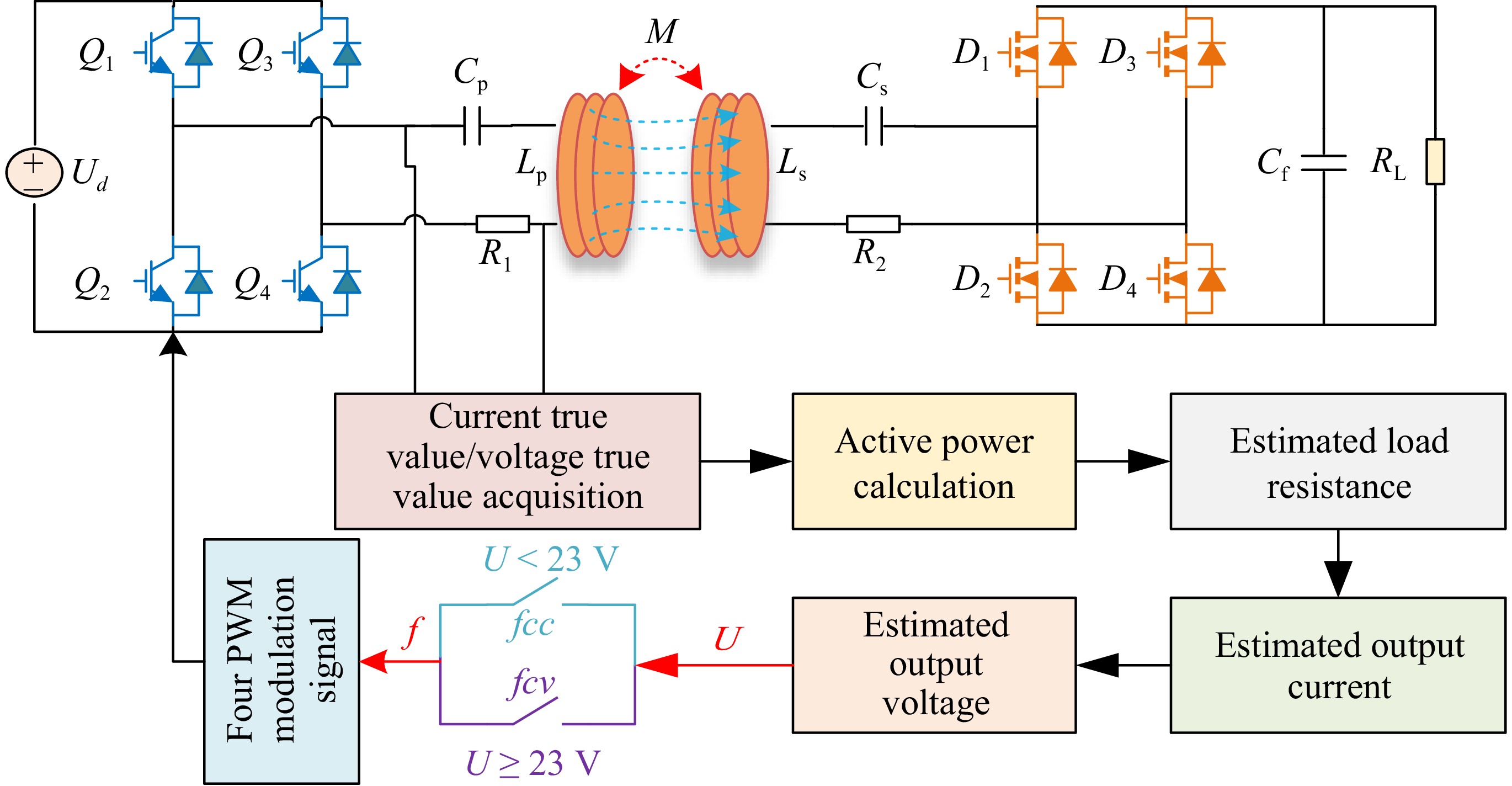
Figure 7.
System switching strategy.
-
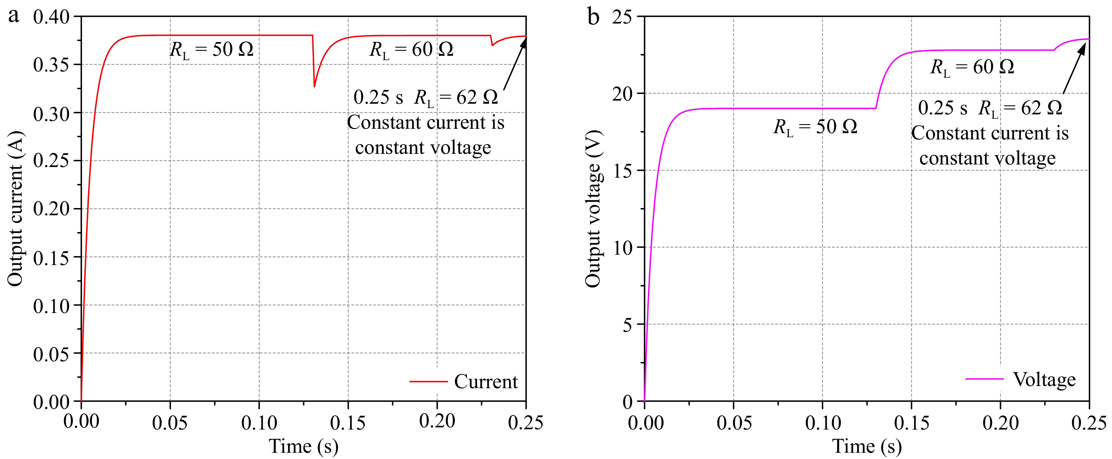
Figure 8.
Current-voltage diagram in constant-current mode. (a) Current. (b) Voltage.
-
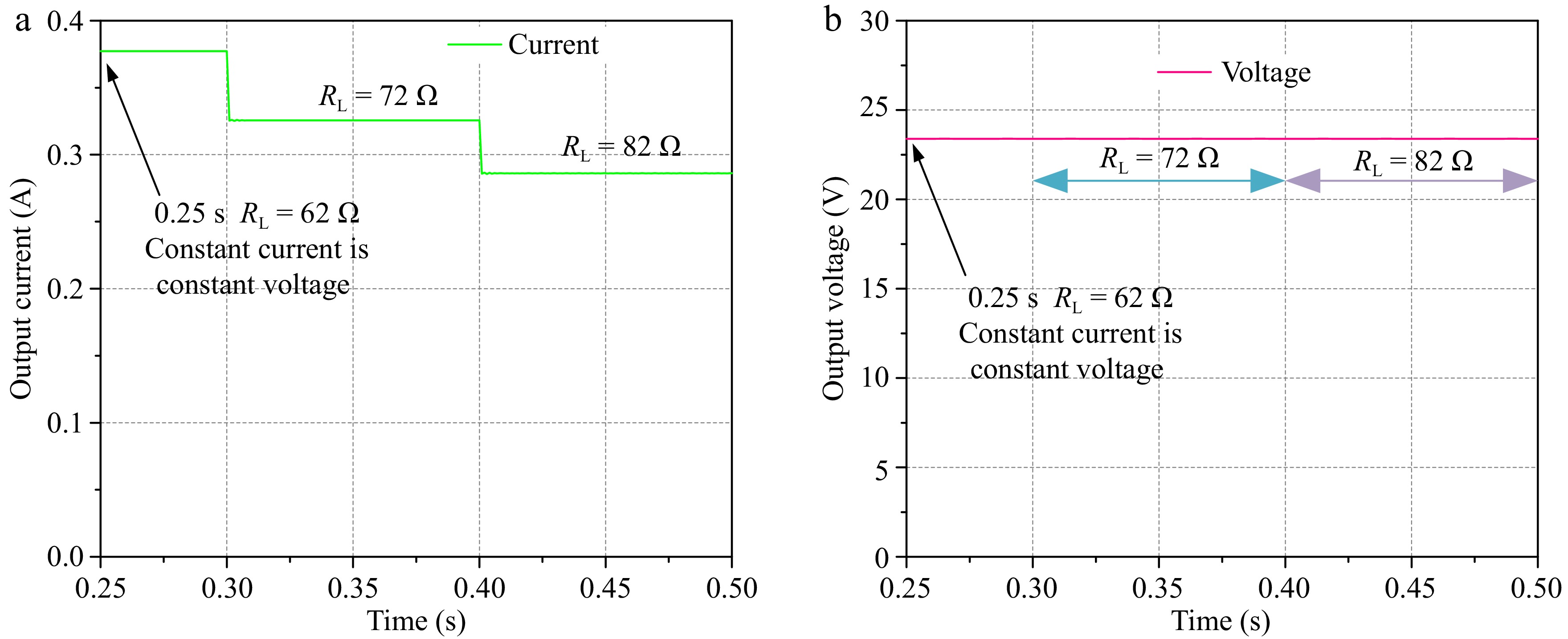
Figure 9.
Current-voltage diagram in constant-voltage mode. (a) Current. (b) Voltage.
-
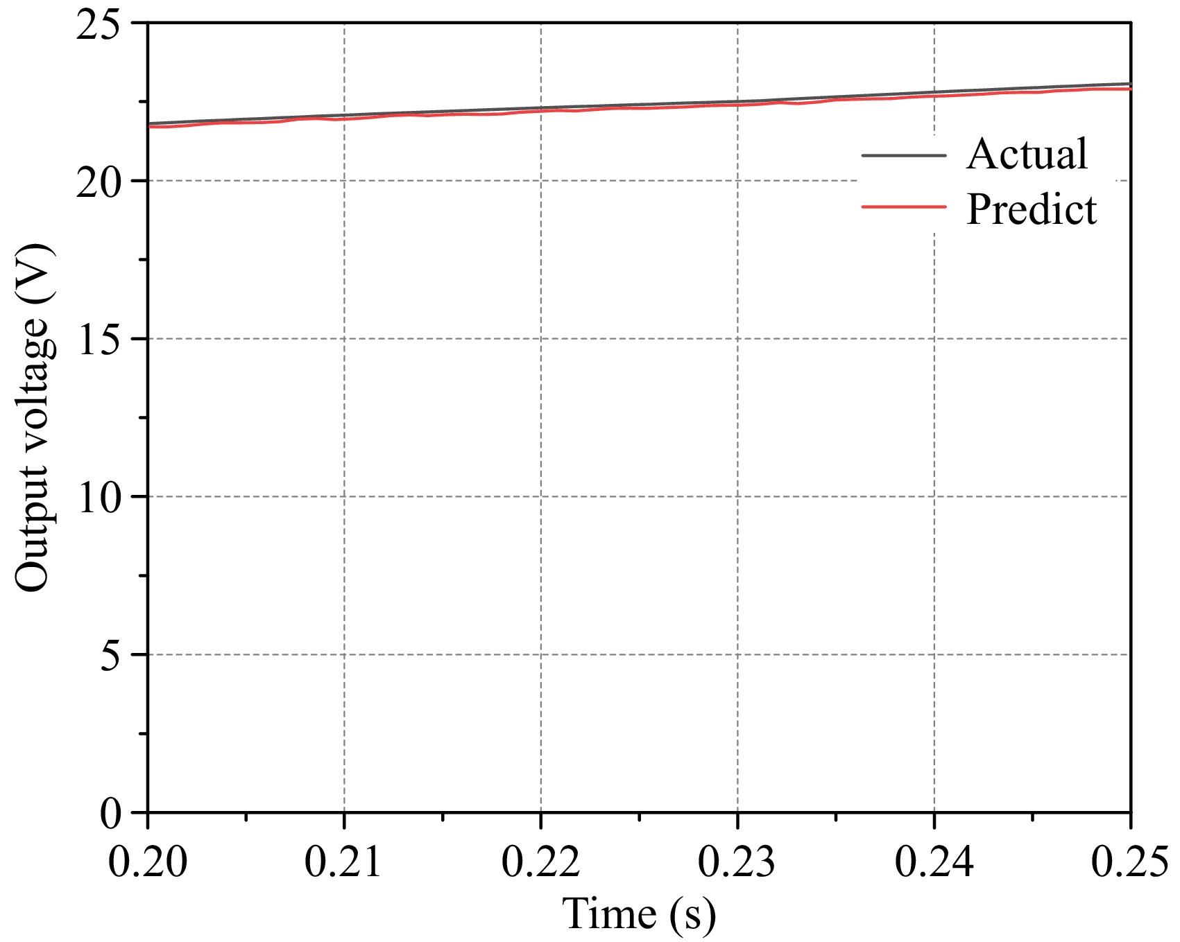
Figure 10.
Predicted and actual voltage waveforms at frequency switching.
-
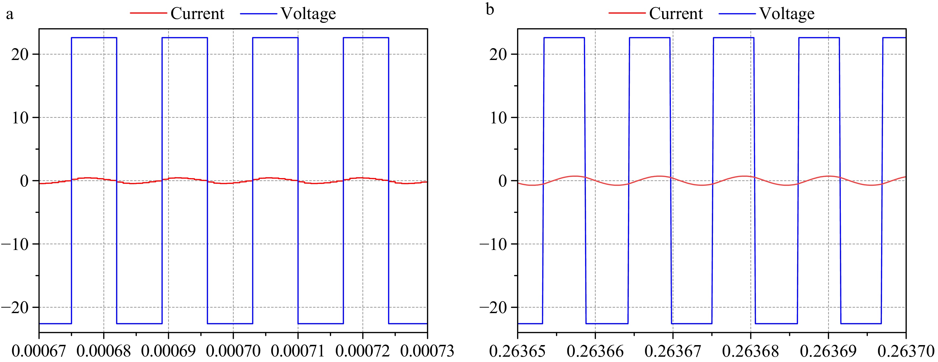
Figure 11.
Voltage-current waveform of inverter output. (a) CC. (b) CV.
-
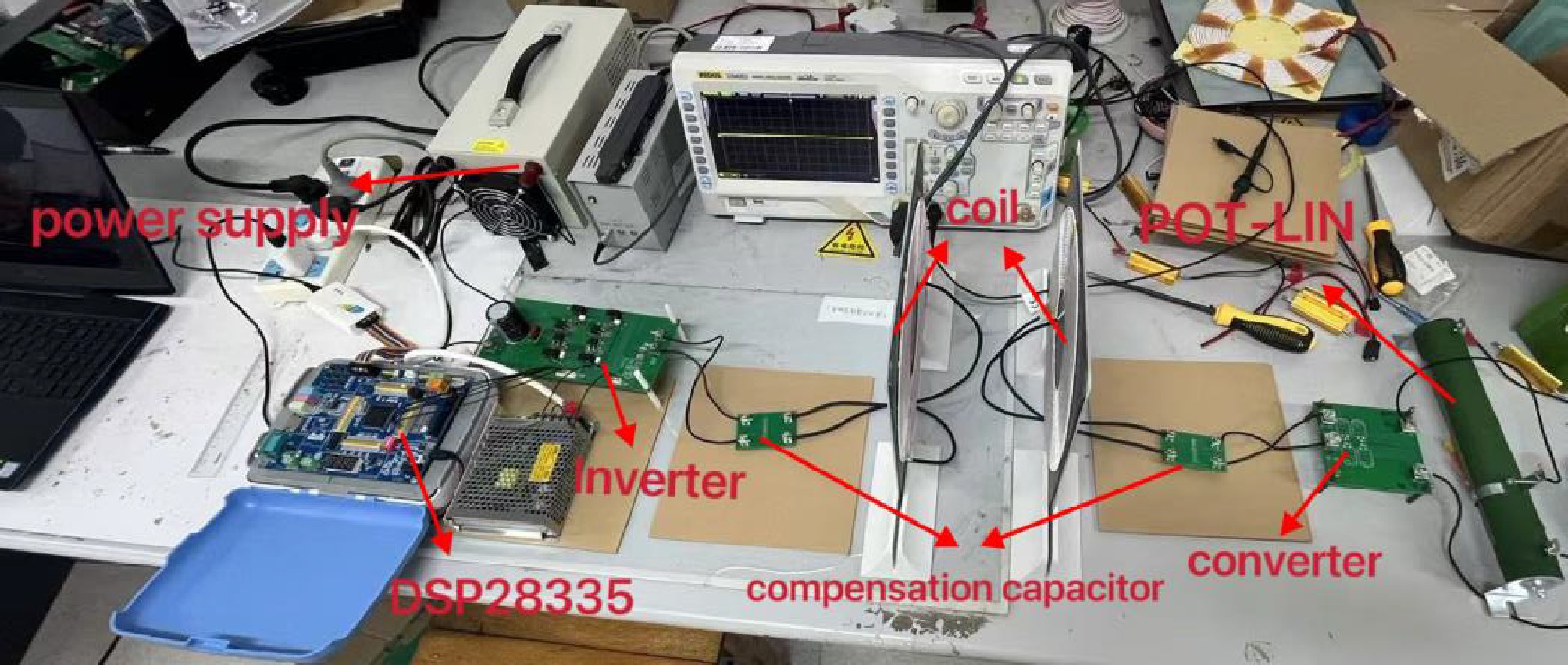
Figure 12.
Experimental platforms.
-
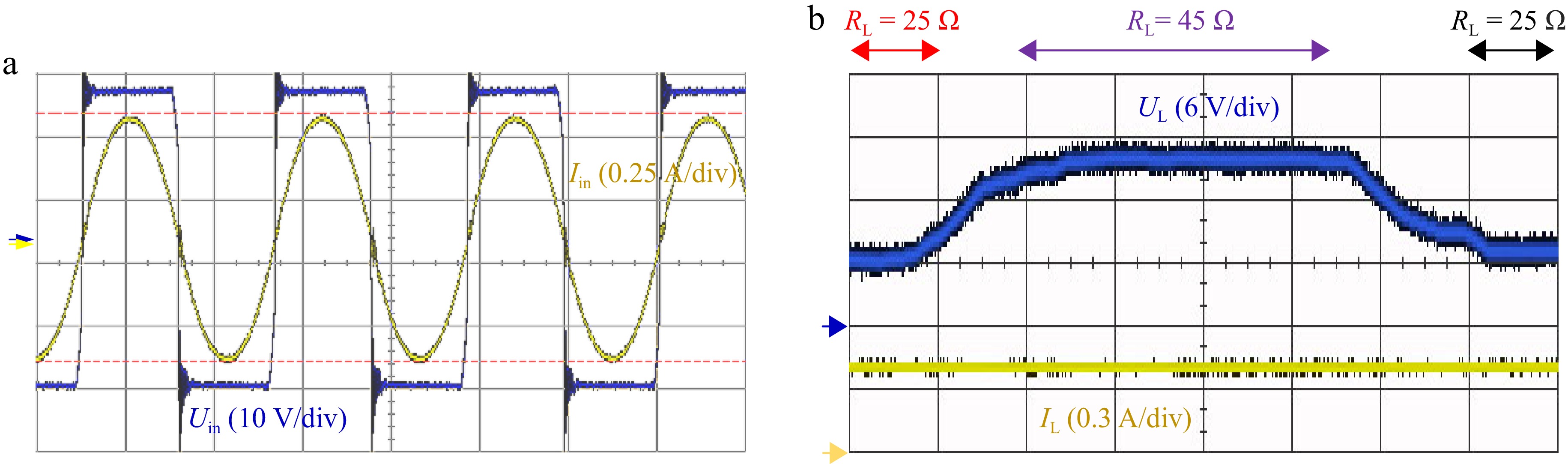
Figure 13.
Experimental diagram of the system in CC mode. (a) Inverter voltage and current phase. (b) Load current and voltage at constant current output.
-
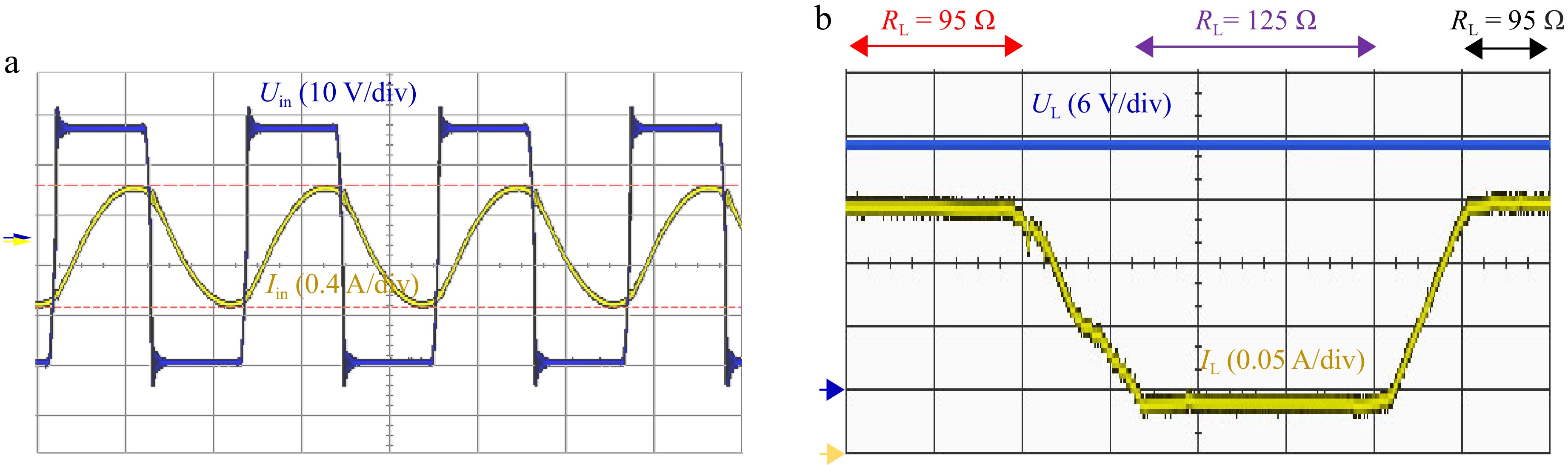
Figure 14.
Experimental diagram of the system in CV mode. (a) Inverter voltage and current phase. (b) Load current and voltage at constant voltage output.
-
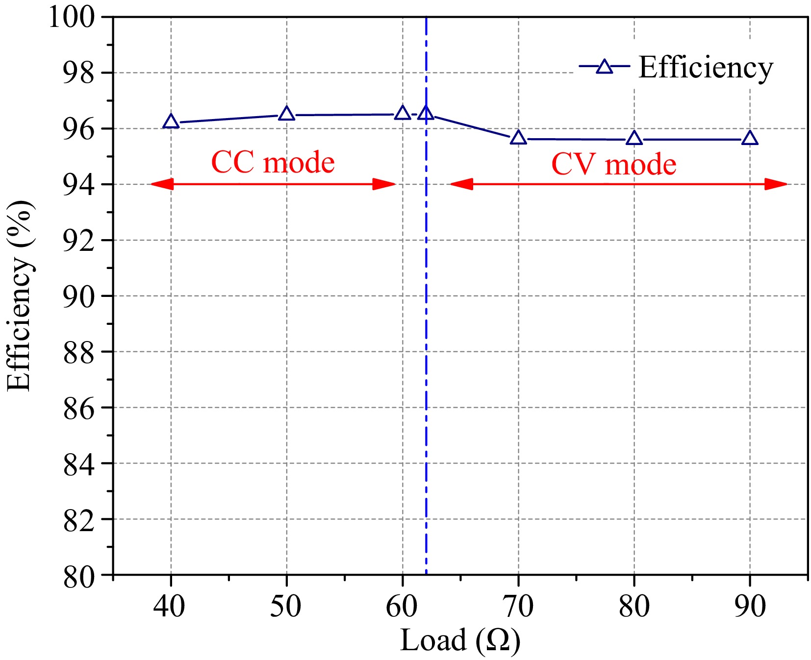
Figure 15.
Efficiency of WPT system with S/S structure.
-
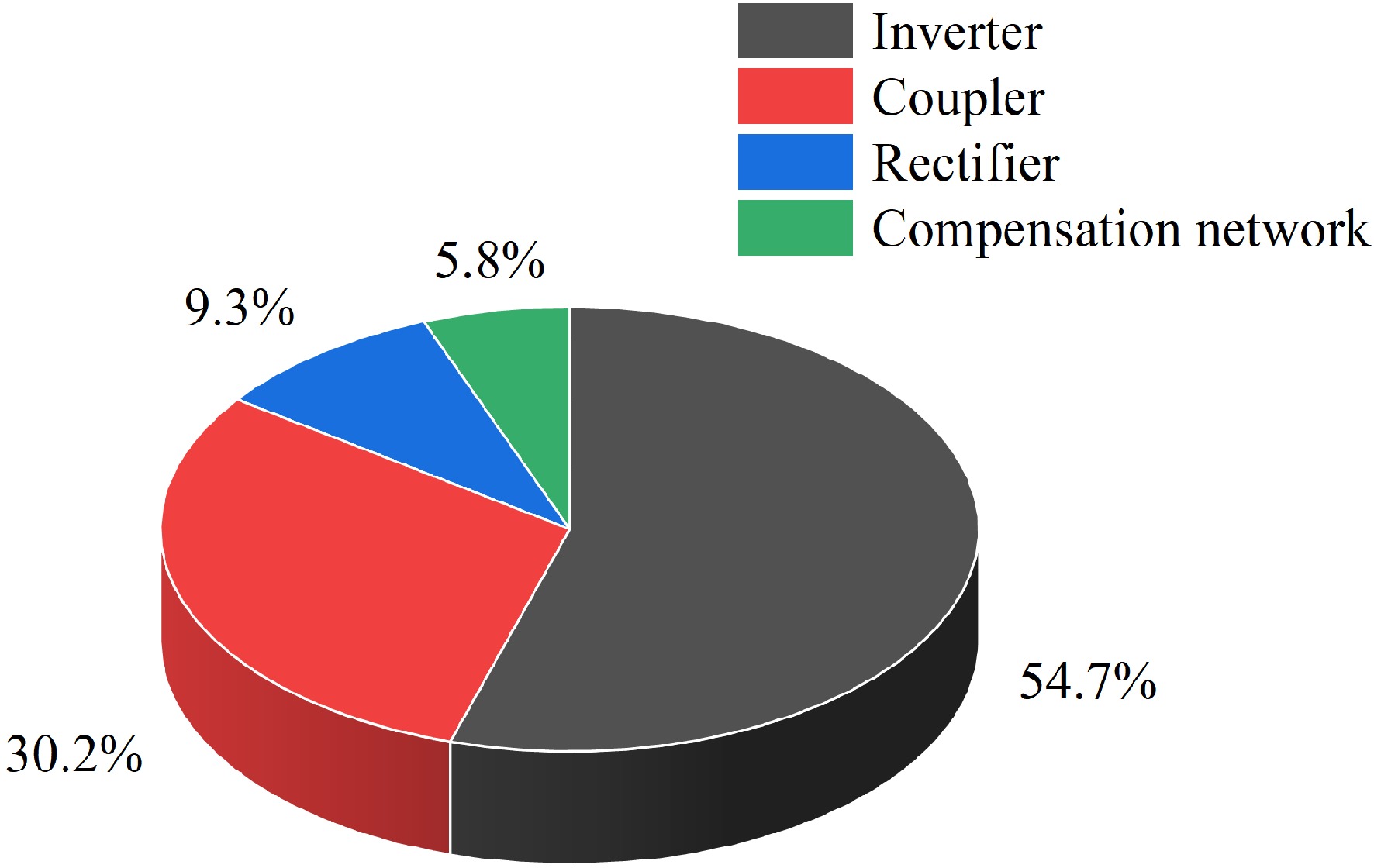
Figure 16.
Analysis of efficiency losses.
-
Parameters Value fcc (kHz) 70 fcv (kHz) 91.7 Cp (nF) 18.546 Cs (nF) 18.221 Lp (μH) 280 Ls (μH) 285 M (μH) 115.918 R1 (Ω) 0.15 R2 (Ω) 0.1 Table 1.
Theoretical circuit parameters.
-
Table 2.
Comparison of CC and CV output WPT systems.
Figures
(16)
Tables
(2)