-
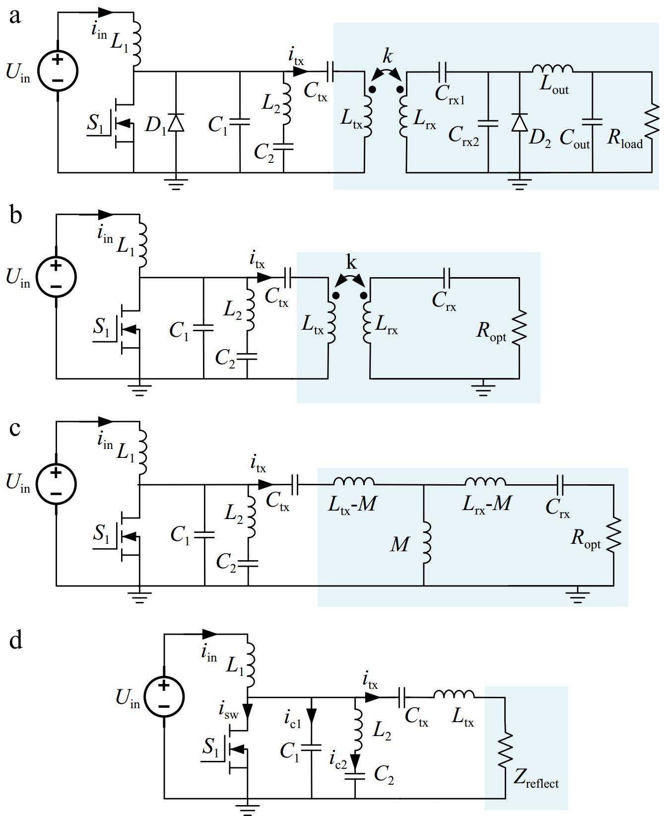
Figure 1.
Circuit of load-independent WPT system design.
-
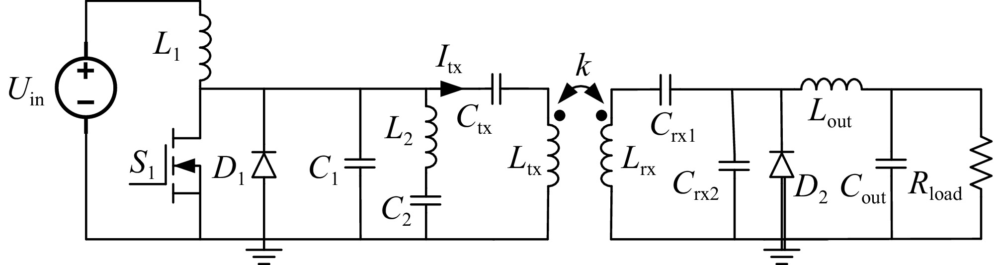
Figure 2.
Proposed 6.78 MHz load-independent WPT system.
-
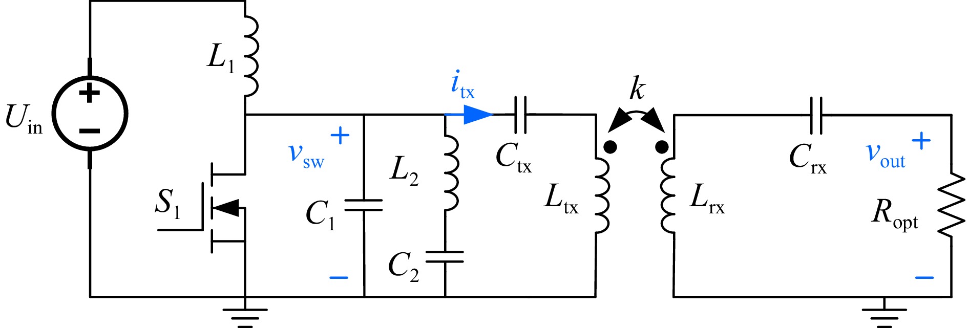
Figure 3.
Simulated circuit diagram of load-independent WPT system.
-
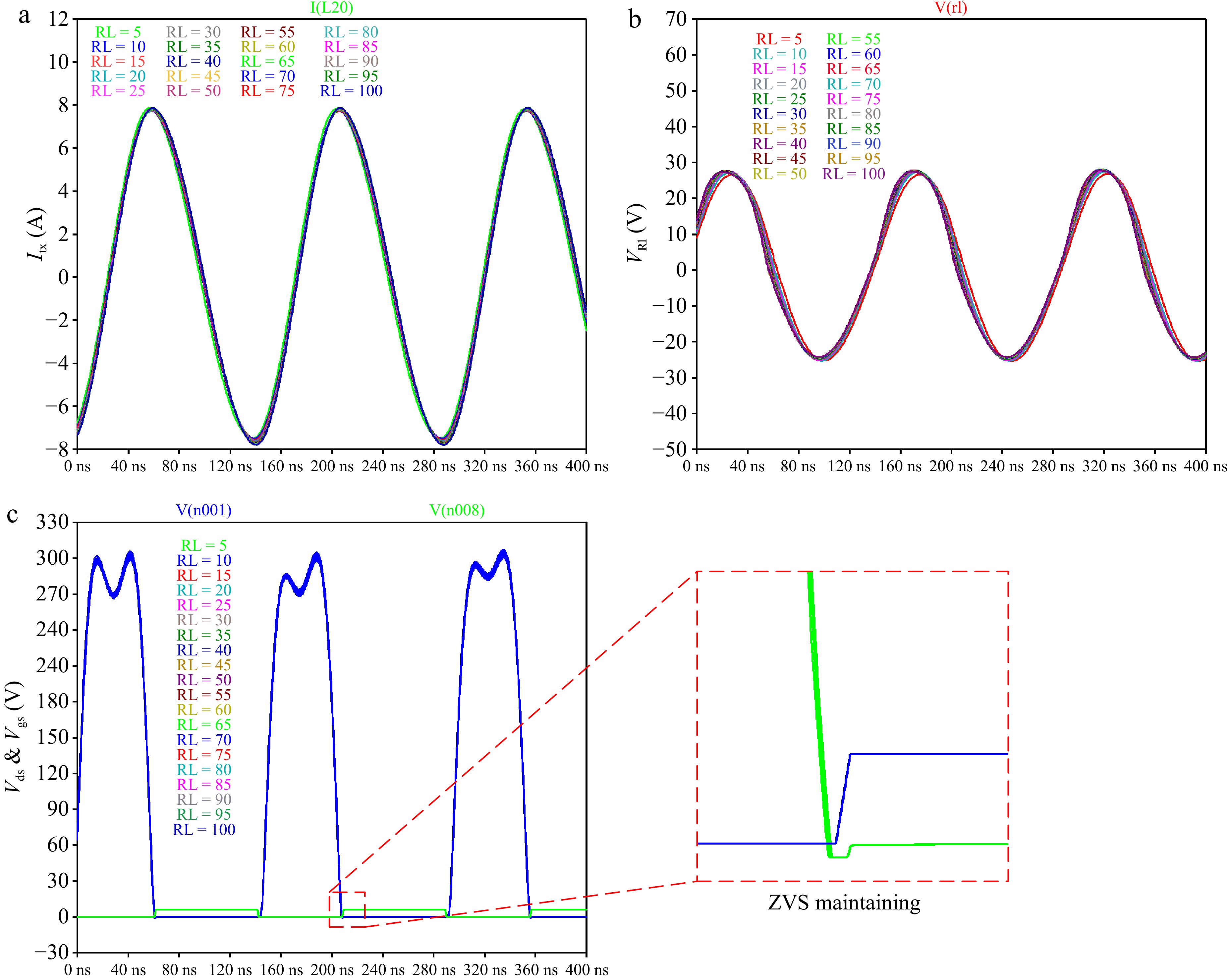
Figure 4.
Simulation TX current and drain-source voltage waveforms and output voltage.
-
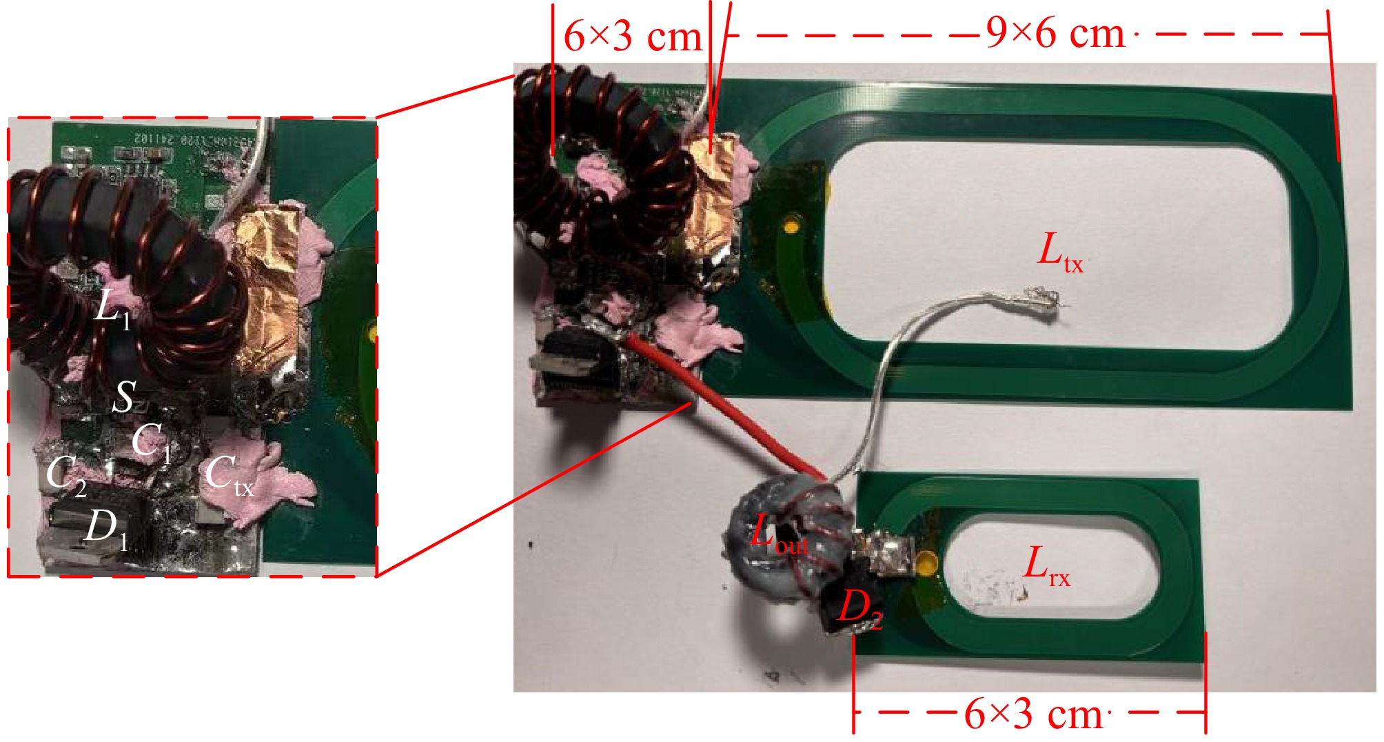
Figure 5.
Proposed load-independent WPT system.
-
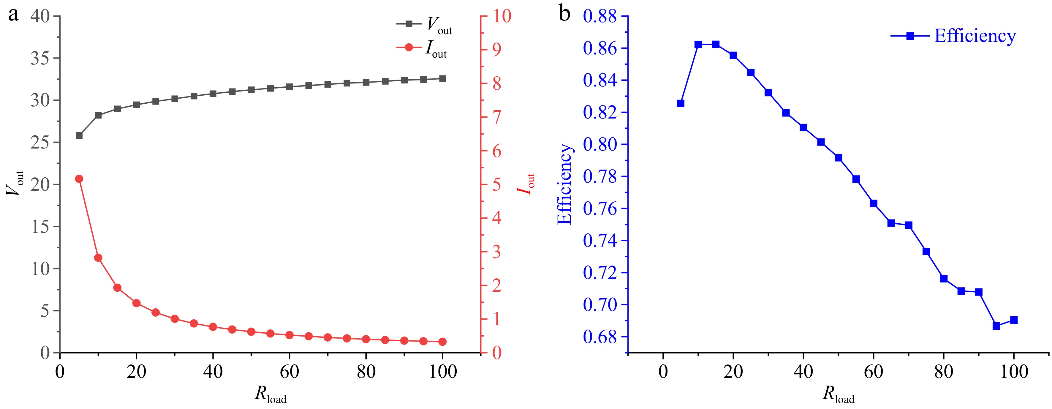
Figure 6.
(a) Experimental output voltage and output current, and (b) system efficiency.
-
Parameter Value Parameter Value Vin 100 v $ {C}_{out} $ 175 nf L1 33 μH $ {C}_{1} $ 160 pf L2 500 nH $ {C}_{2} $ 130 p Ltx 2.25 μH $ {C}_{tx} $ 310 p Lrx 266 nH $ {C}_{rx} $ 2.6 nf Lout 1.8 μH $ {C}_{rx2} $ 2.6 nf Table 1.
Parameters of the MIMO WPTN system.
Figures
(6)
Tables
(1)