-
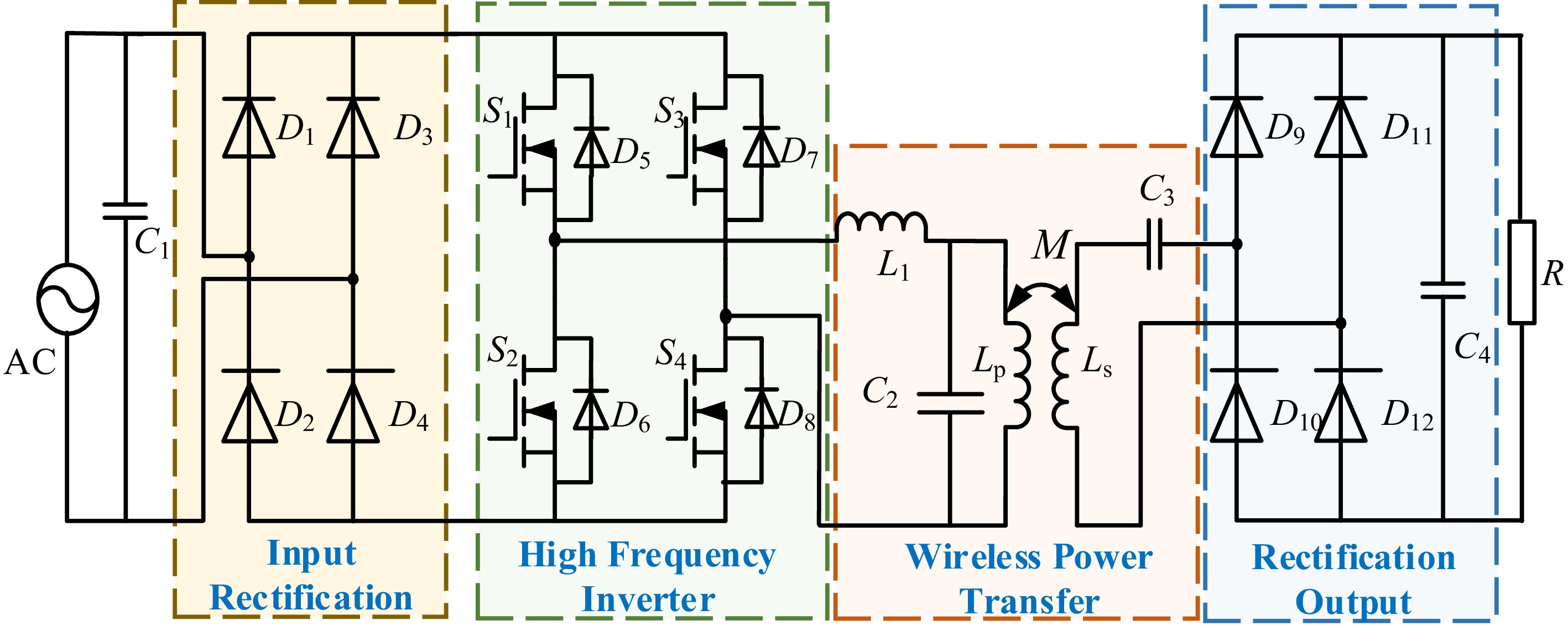
Figure 1.
Main circuit topology.
-
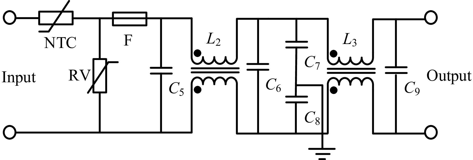
Figure 2.
Rectification and filtering circuit diagram.
-
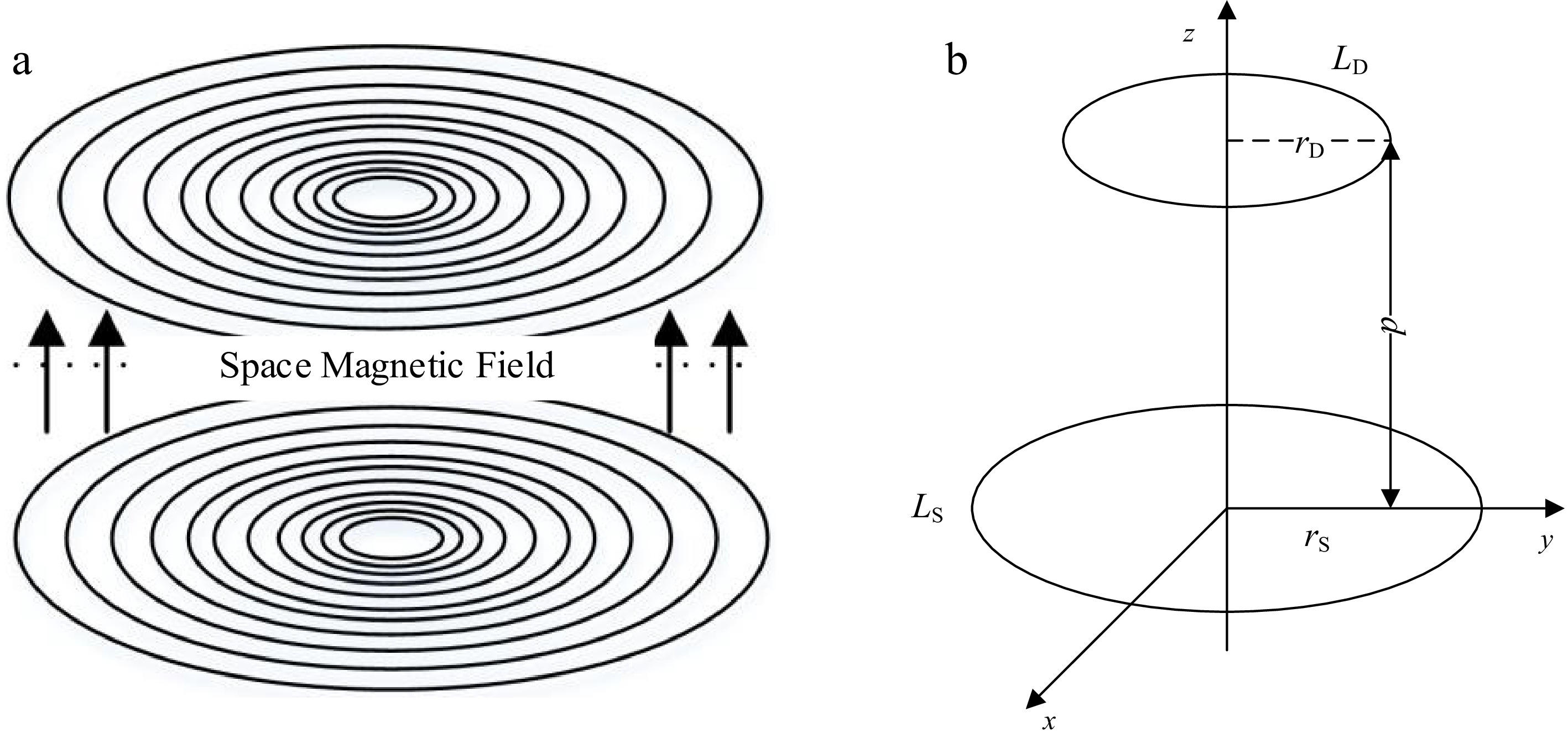
Figure 3.
Diagram of WPT coil. (a) Diagram of planar coil structure. (b) Diagram of parallel coaxial coil spatial structure.
-
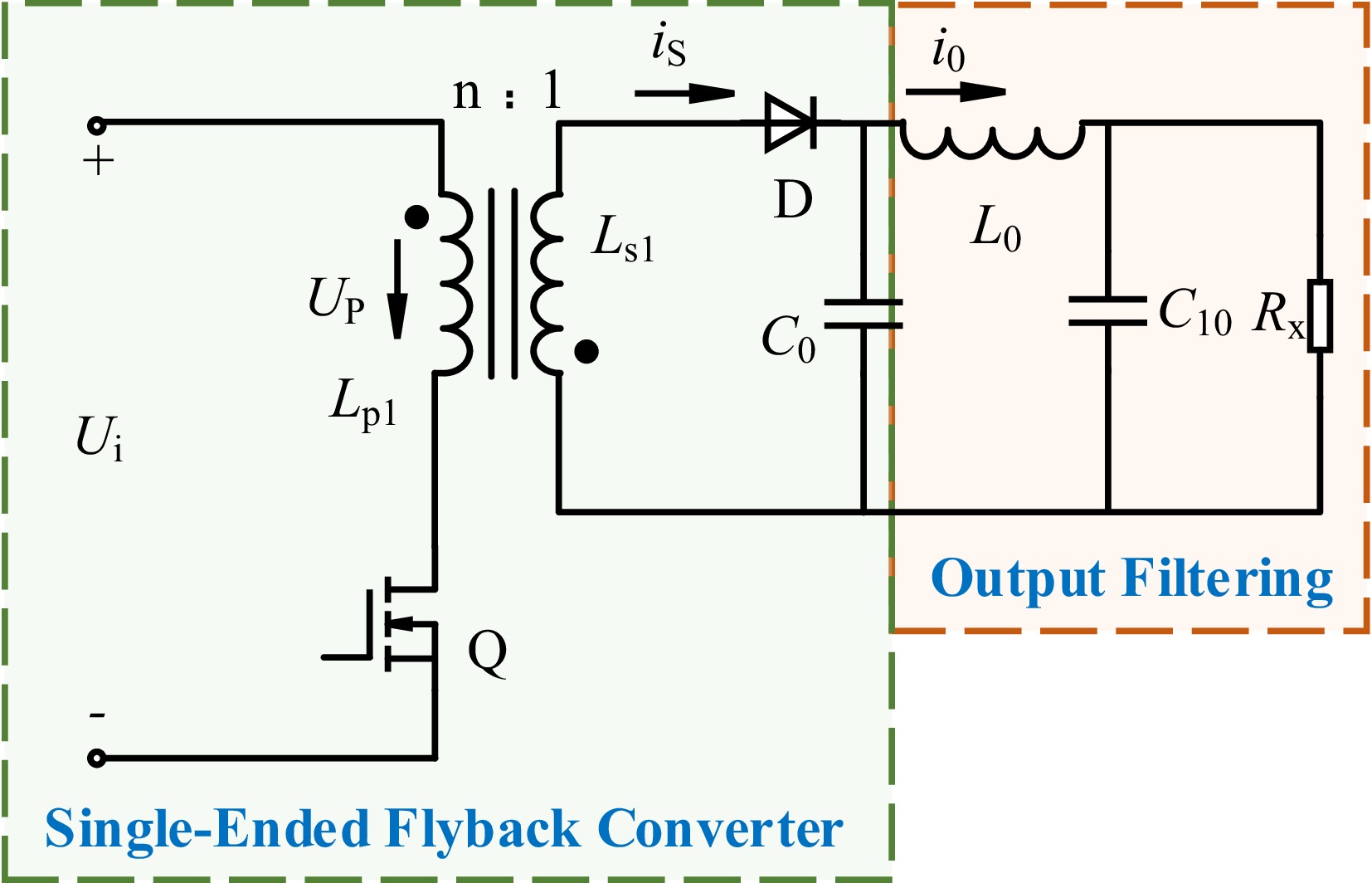
Figure 4.
Single-ended flyback converter with output filtering.
-
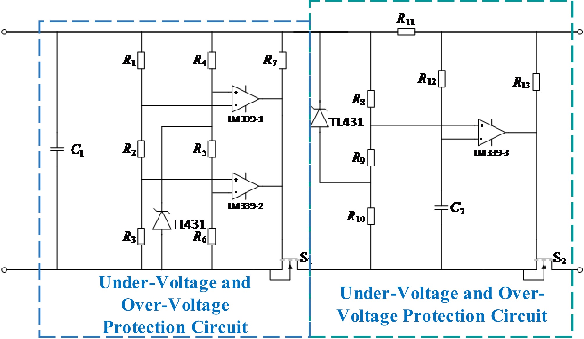
Figure 5.
Single-ended flyback converter with output filtering.
-
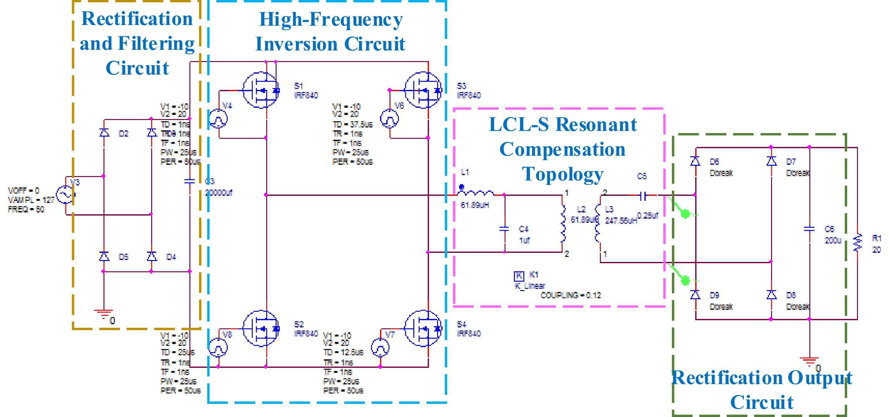
Figure 6.
Diagram of main circuit simulation.
-
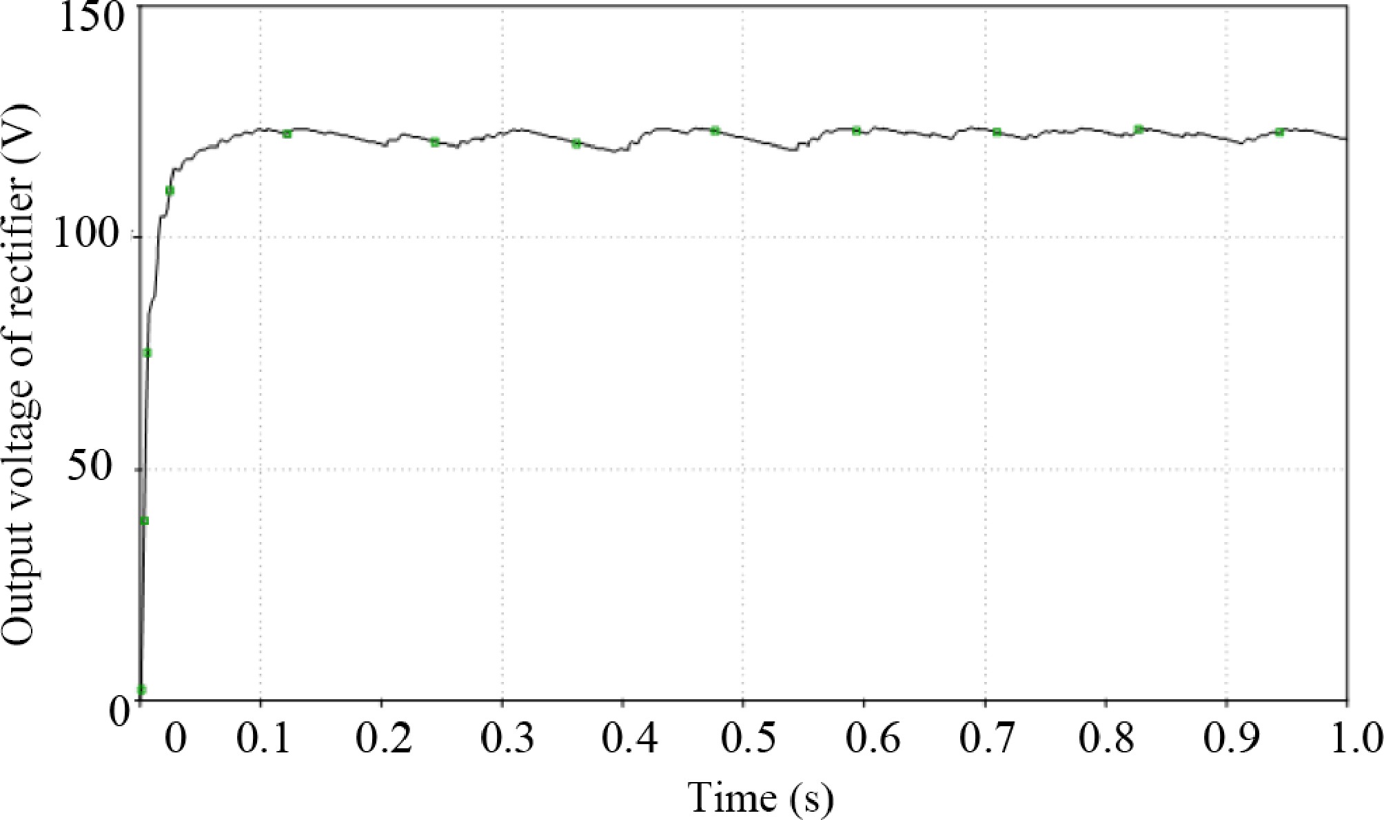
Figure 7.
Waveform of rectified output voltage.
-
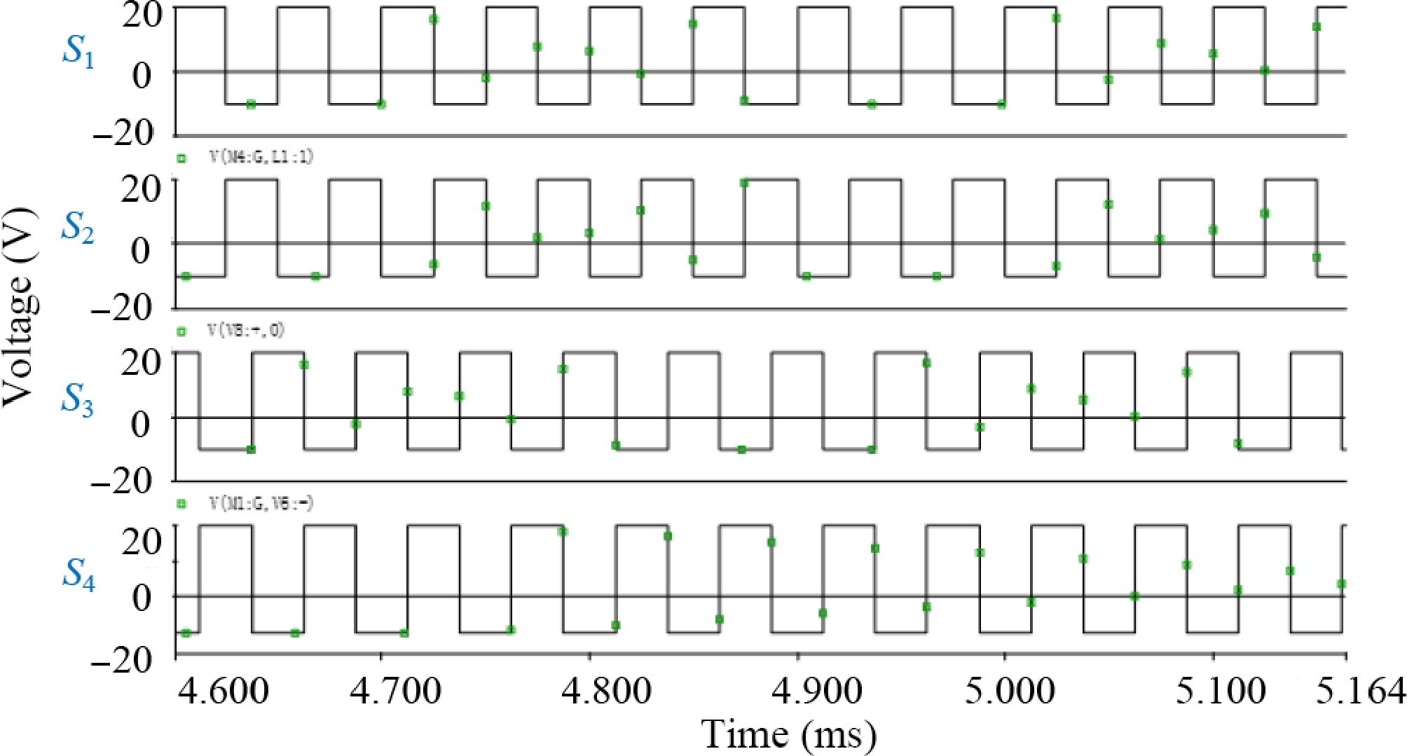
Figure 8.
Waveform of phase shift control pulse.
-
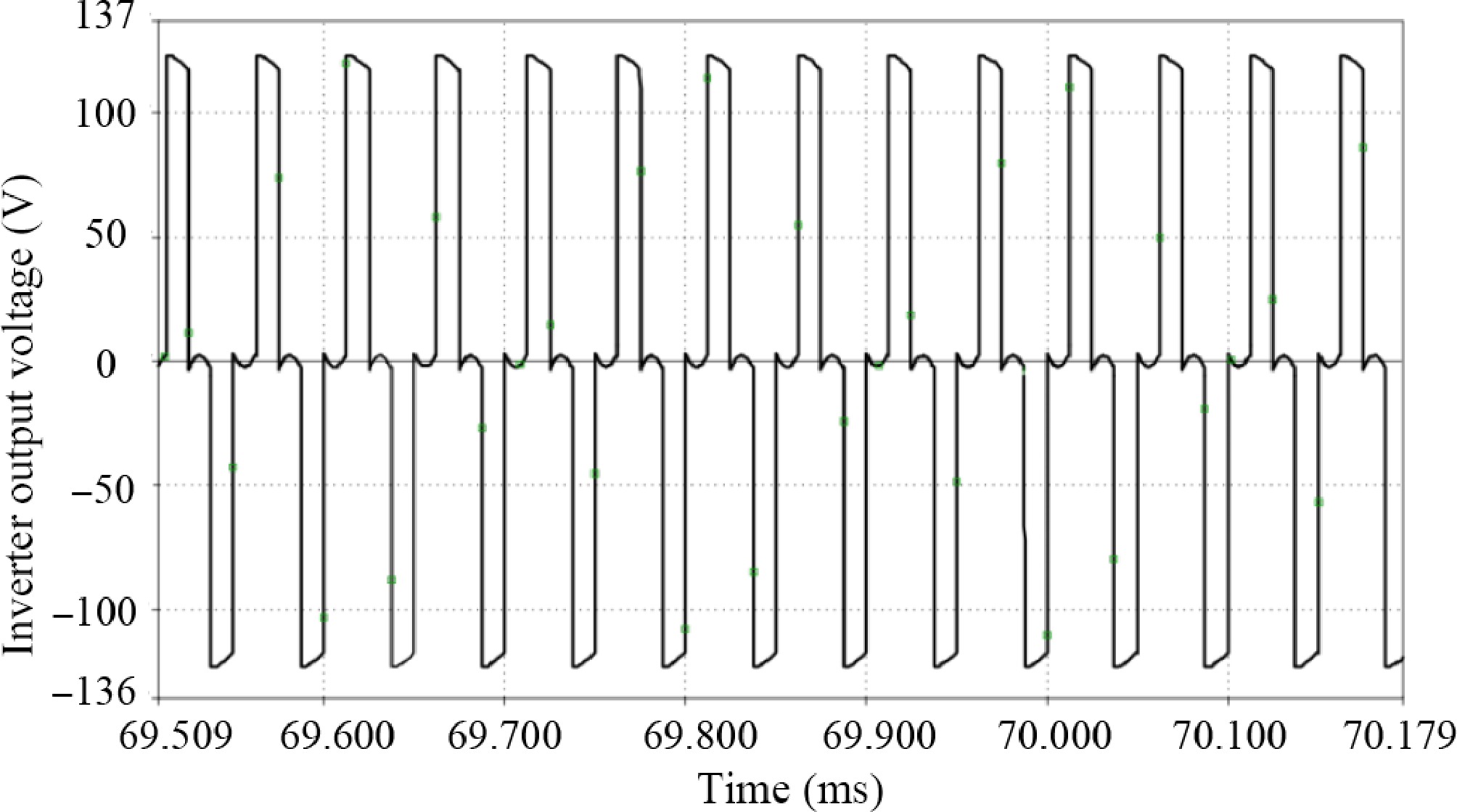
Figure 9.
Waveform of inverter circuit output.
-
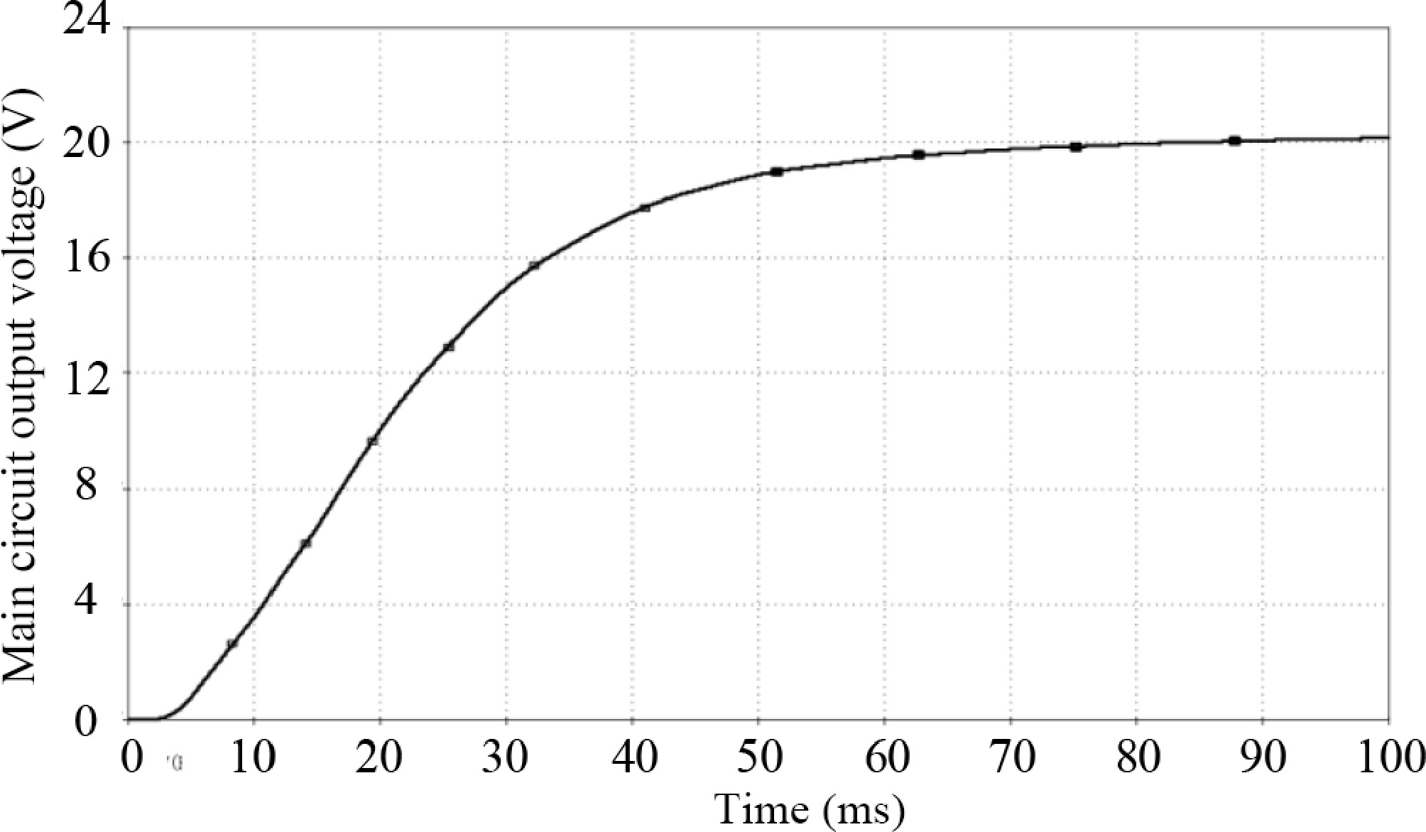
Figure 10.
Waveform of main circuit output.
-
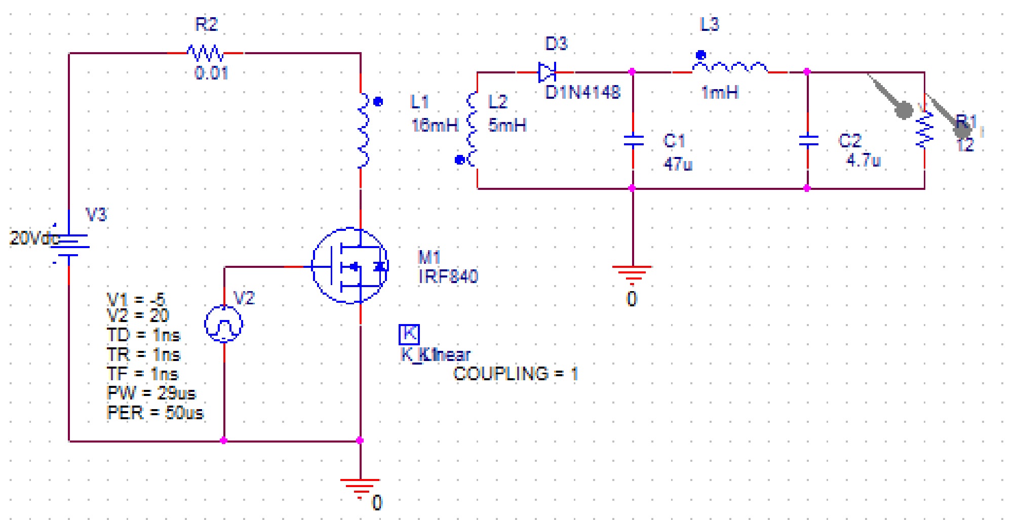
Figure 11.
Single-ended flyback DC-DC converter.
-
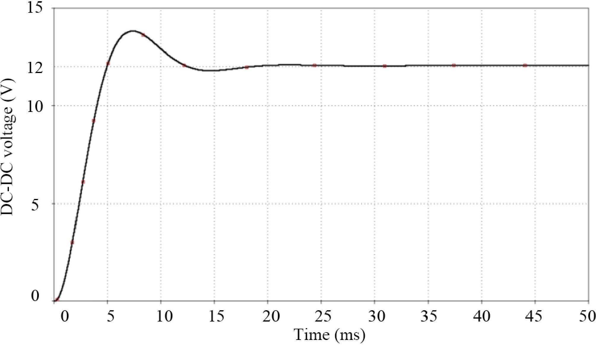
Figure 12.
Result of DC-DC voltage regulation simulation.
-
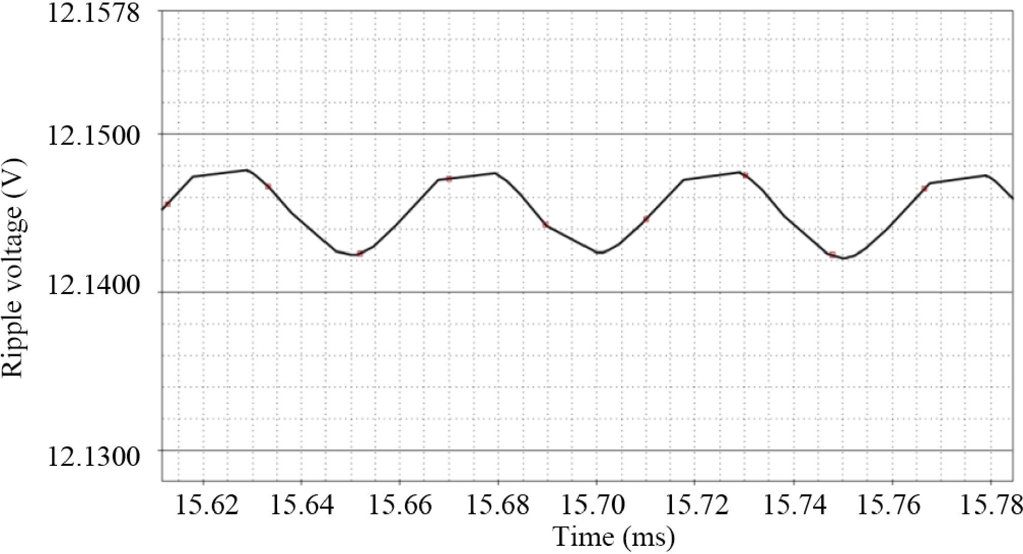
Figure 13.
Waveform of output voltage ripple.
-
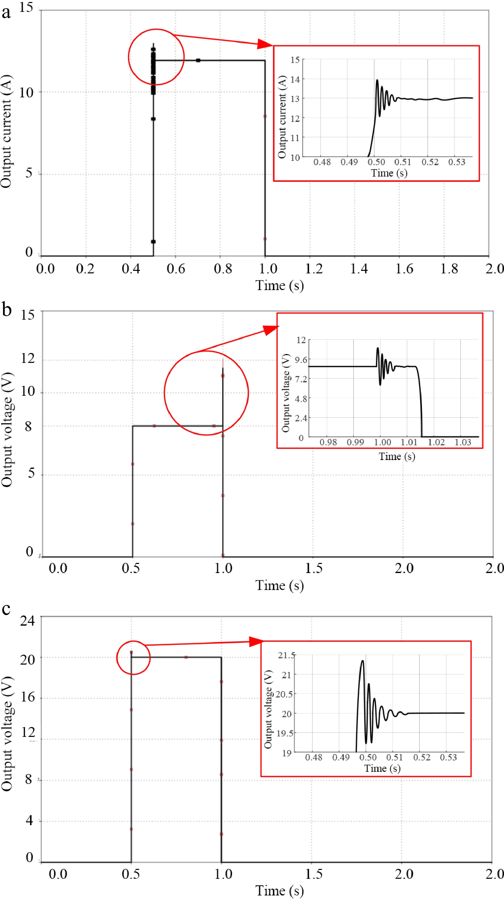
Figure 14.
Results of the protection circuit experiment. (a) Overcurrent protection simulation result. (b) Undervoltage protection simulation result. (c) Overvoltage protection simulation result.
-
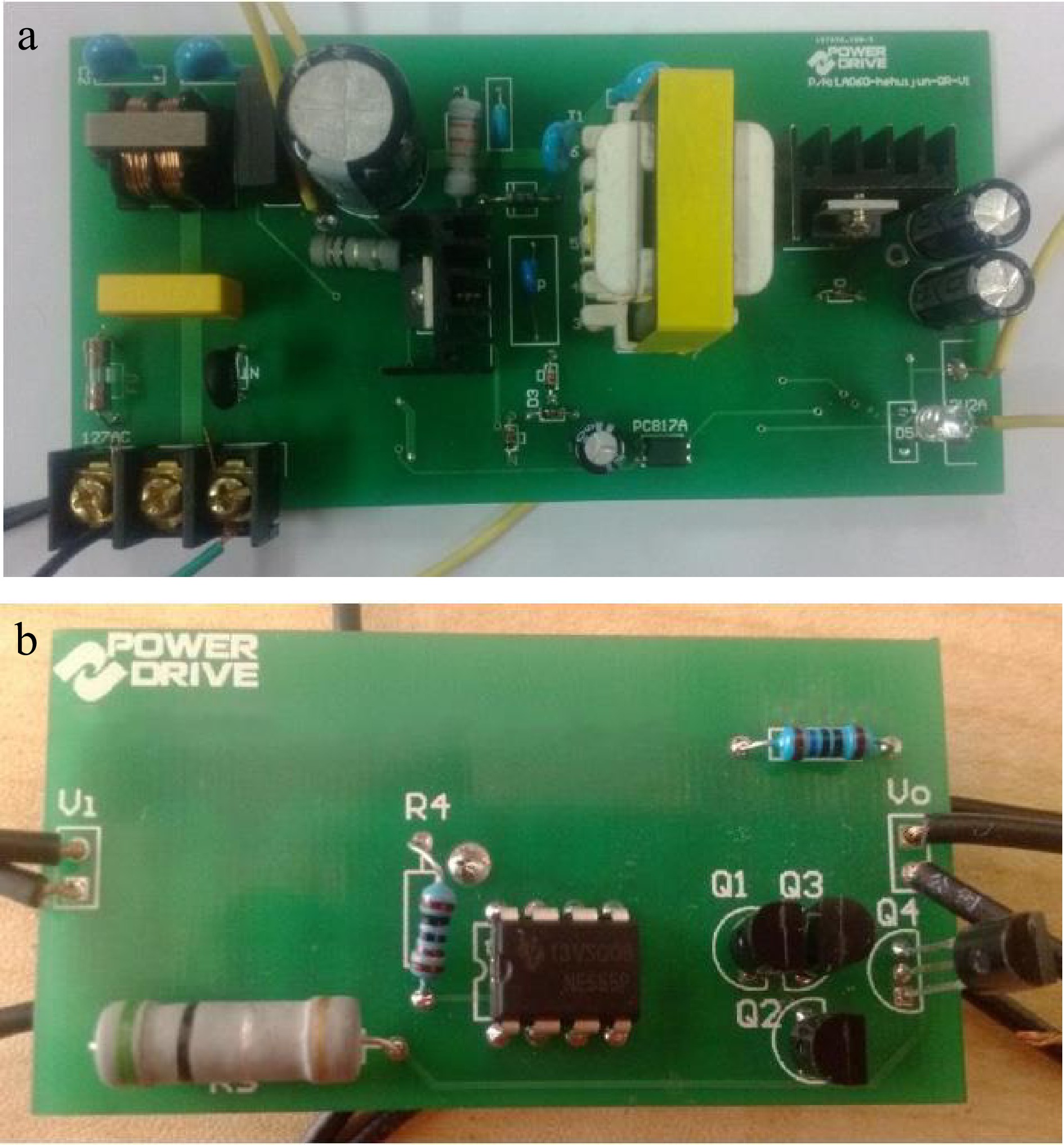
Figure 15.
Prototype of the improved clamping-based single-stage flyback converter. (a) Single-stage flyback converter. (b) Improved clamping-based protection circuit.
-
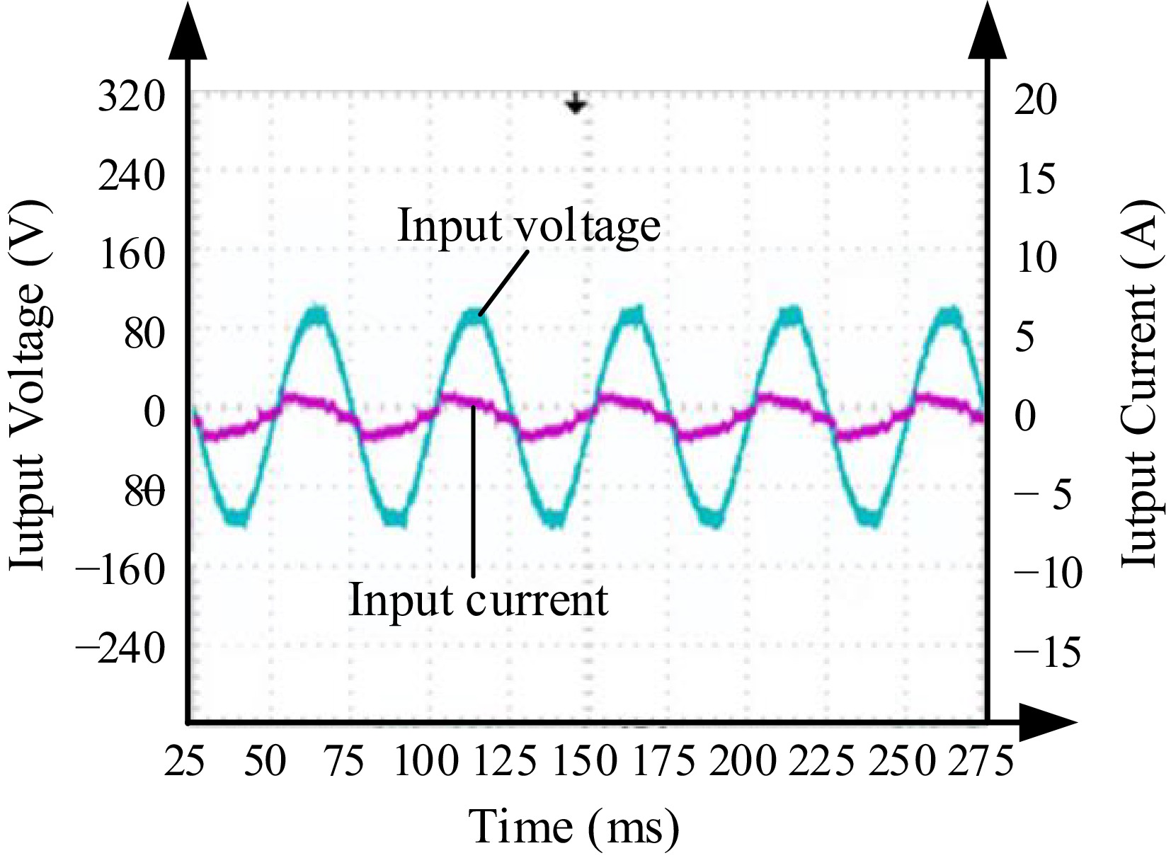
Figure 16.
Waveform of the input voltage and current.
-
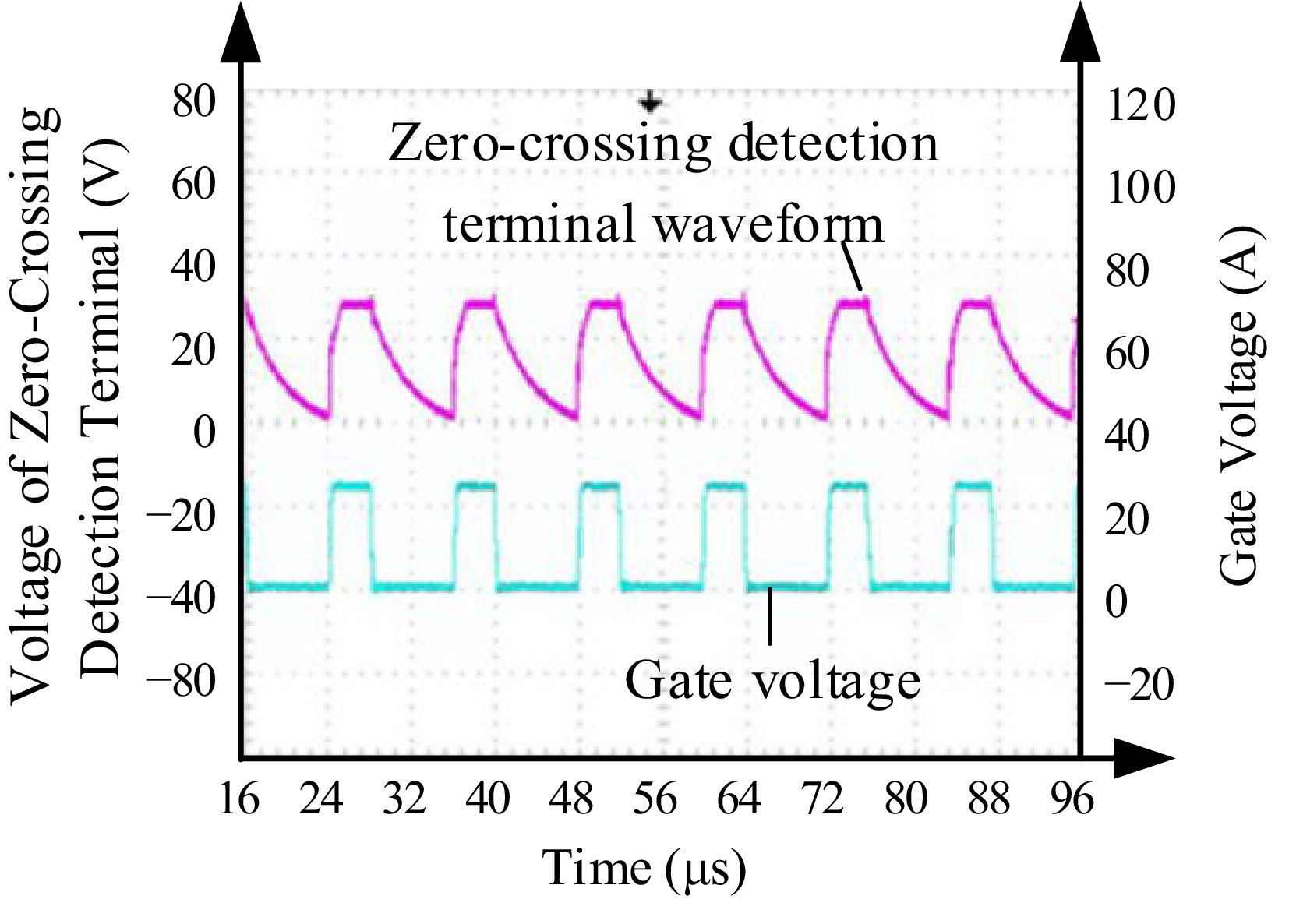
Figure 17.
Waveform of the gate voltage and the zero-crossing detection terminal.
-
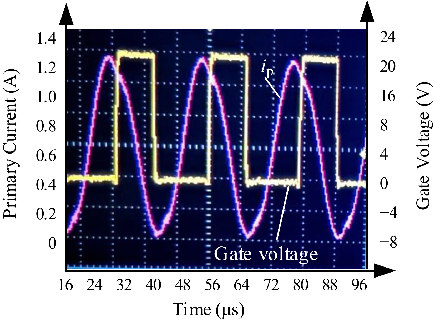
Figure 18.
Waveform of inverter control voltage and WPT system primary current.
-
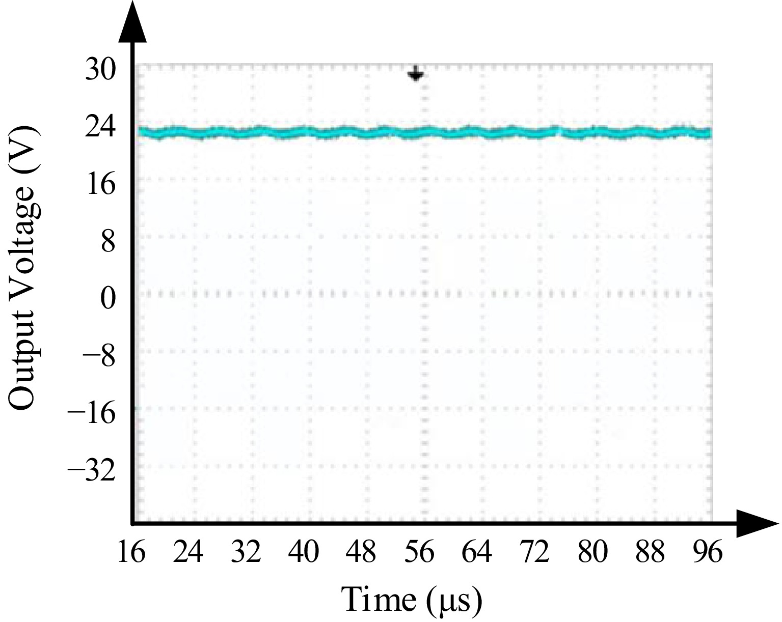
Figure 19.
Waveform of the output voltage.
-
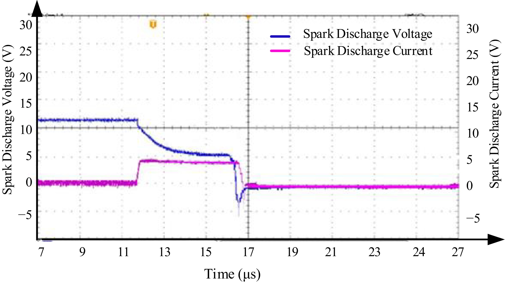
Figure 20.
The waveform of the ameliorated cutoff experiment.
-
Parameter Single-ended fly-back converter Full-bridge converter Efficiency Moderate (85%−90%) High (90%−95%) Cost Low High Complexity Low High Failure points Few Multiple Suitability for harsh environments High Moderate Table 1.
Comparison of the single-ended flyback converter with a full-bridge converter.
-
Parameter Value Parameter Value Vinmax 150 V R4 5 kΩ IBF 0.14 A R5 and R6 1 kΩ UDS 200 V R7 10 kΩ ID 6 A R8 1.3 kΩ Ui 20 V R9 3.3 kΩ Uo 12 V R10 1 kΩ Dmax 0.545 R11 0.7 kΩ R1 9.7 kΩ R12 10 kΩ R2 1 kΩ R13 1 kΩ R3 1.3 kΩ Cp 1 μF La and Lp 61.89 μH Cs 0.25 μF Ls 247.56 μH C1 47 μF L3 1 mH C2 4.7 μF C3 0.25 μF C4 200 μF Table 2.
System parameter configuration table.
-
Technology Safety and reliability Output of voltage and power Ref. Laser power converters (LPC) Emphasis on efficiency and safe conversion technology Conversion efficiency: 33.8%, laser power input: 1 mW [17] Hybrid front-end converters, ultracapacitors, sodium-based batteries Ensures reliable operation and harmonic reduction Energy storage capacity: 3 MJ, peak power: 24 MW, load cycle: 10–60 s [18] Single-ended flyback converters, voltage regulation, protection circuits Intrinsically safe design, rapid response to anomalies Output voltage: 12 V, ripple: < 120 mV, protection response: 5 µs This article Table 3.
Comparison between WPT system and other mining power systems.
Figures
(20)
Tables
(3)