-
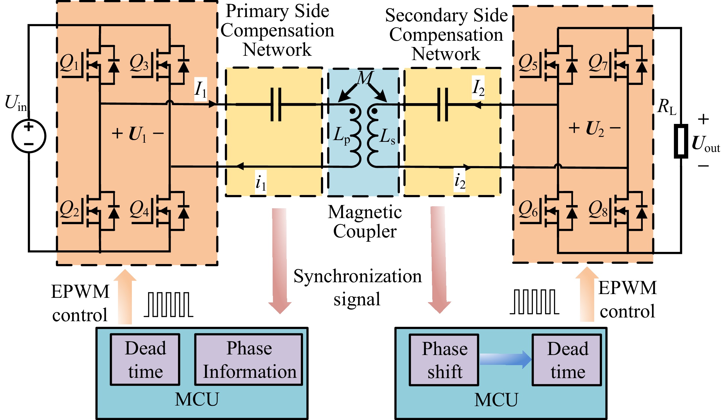
Figure 1.
A typical structure block diagram of the BWPT system.
-

Figure 2.
Equivalent circuit of the BWPT system.
-

Figure 3.
Phase-shift modulation-based power control strategy for the S–S compensation topology.
-
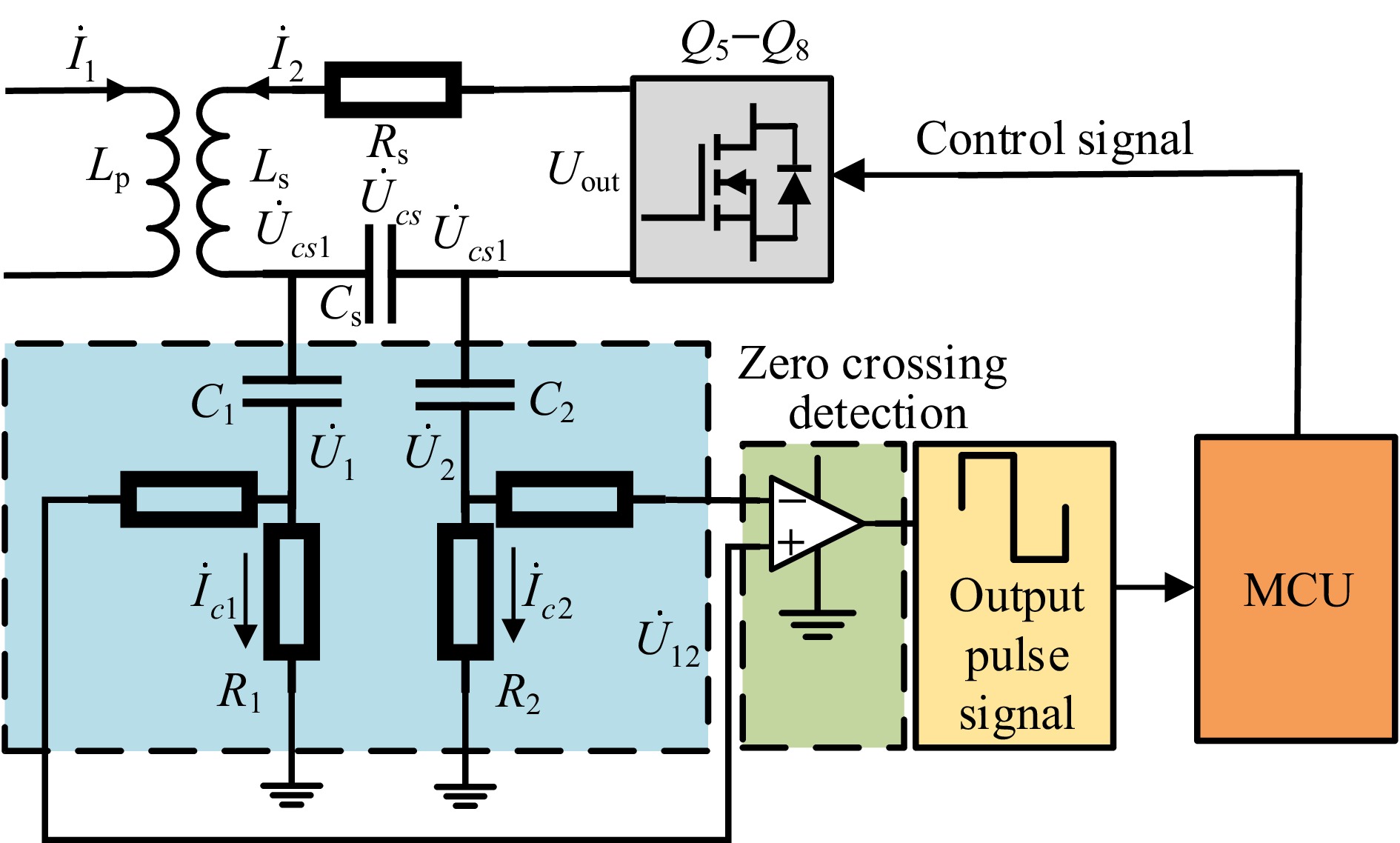
Figure 4.
Diagram of the circuit of the zero-crossing detection.
-
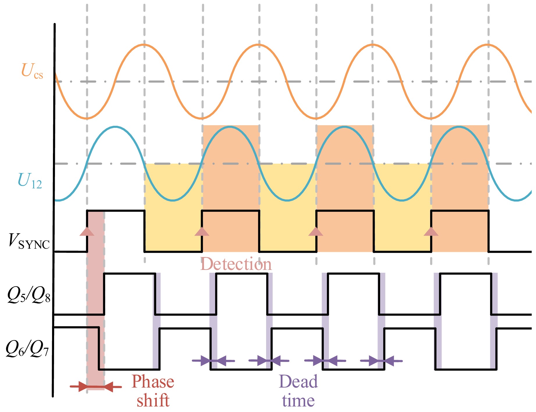
Figure 5.
Time sequence diagram of the proposed SR method signal.
-
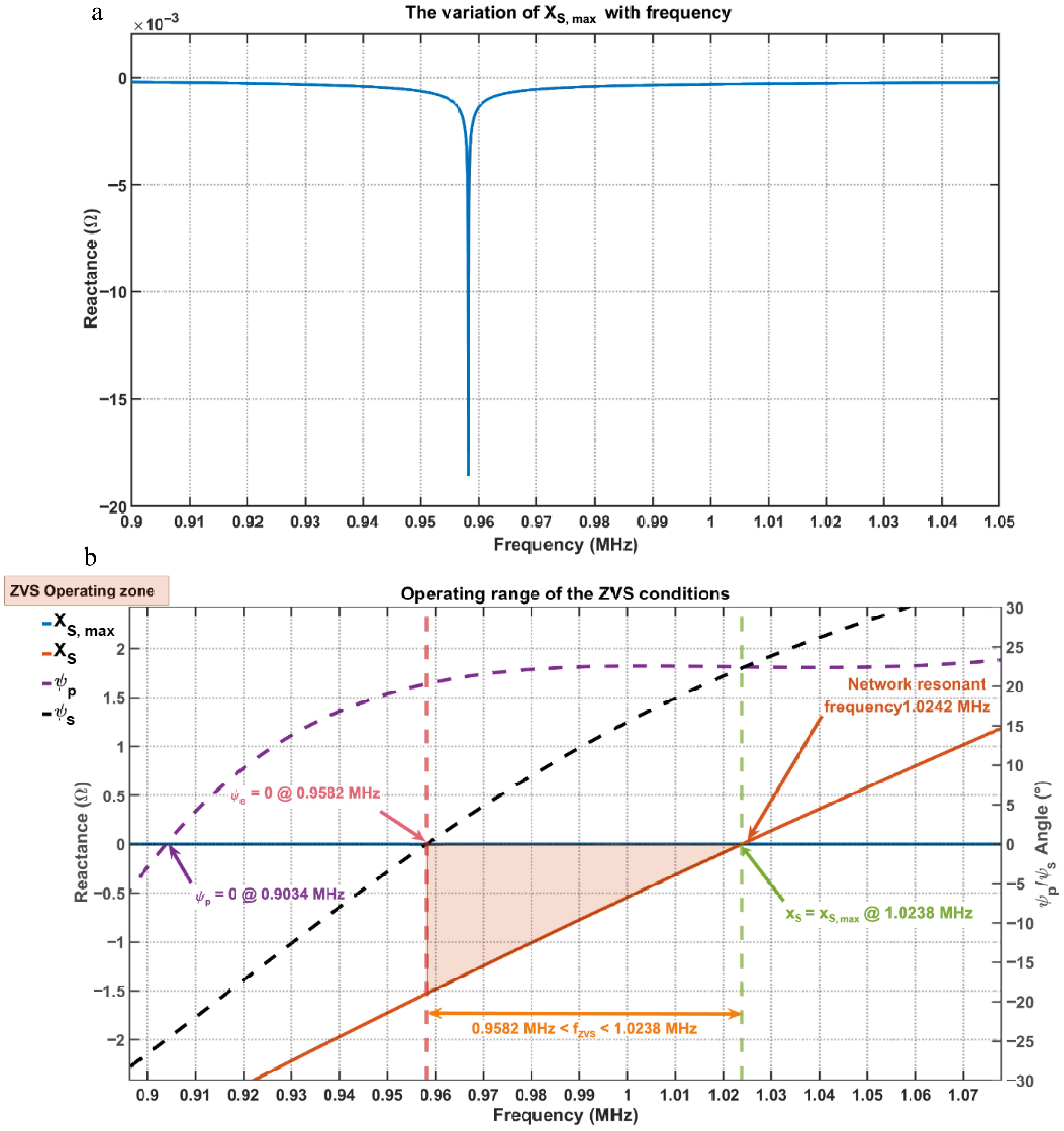
Figure 6.
Operating range of the ZVS conditions. (a) The variation of XS,max with frequency. (b) The range of ZVS.
-
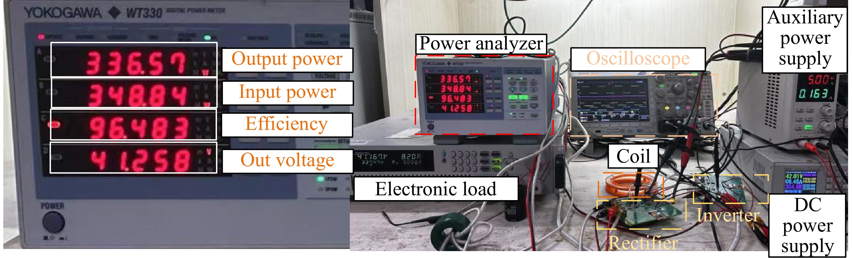
Figure 7.
Experimental platform and max efficiency.
-
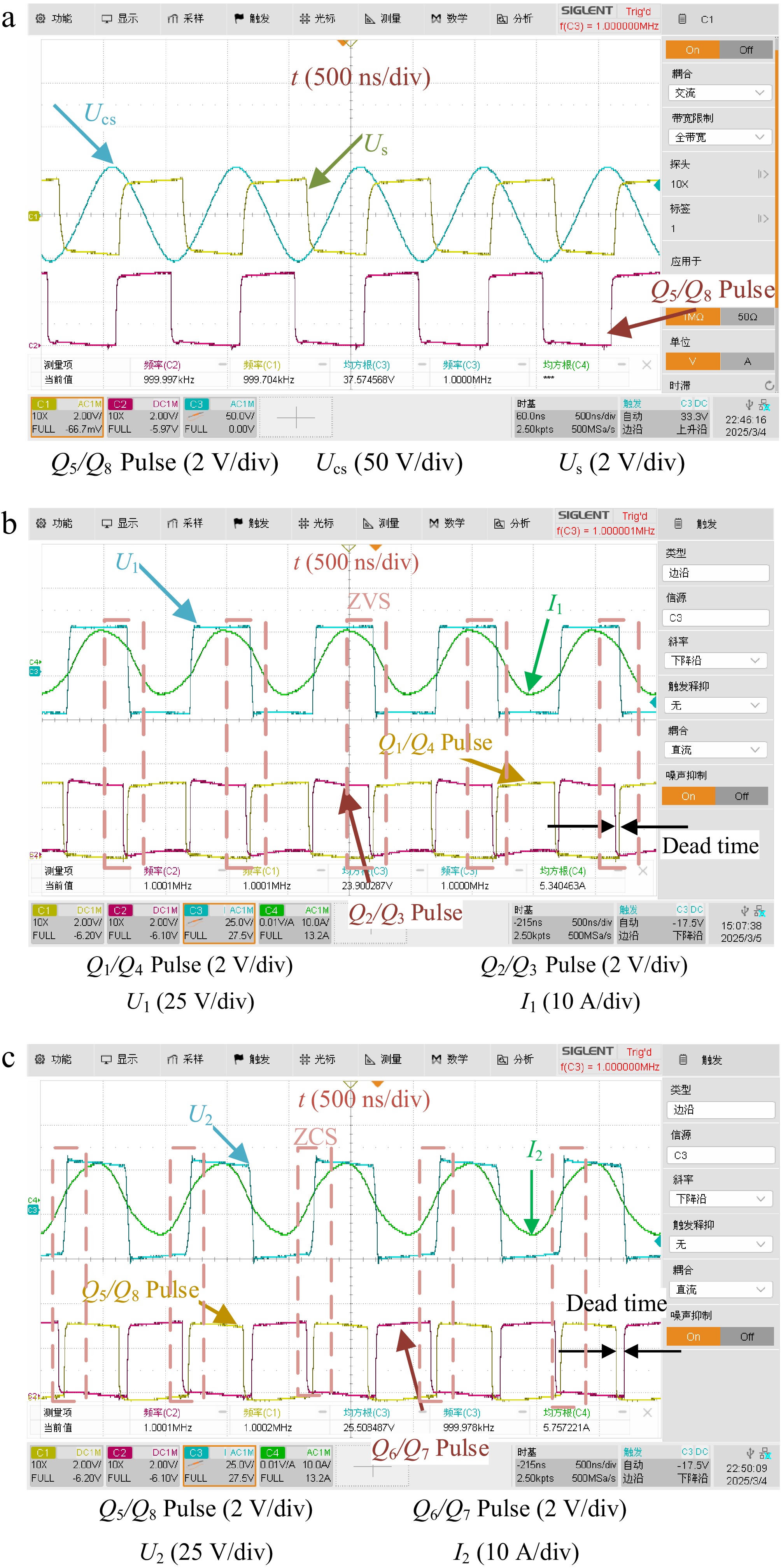
Figure 8.
Soft-switching and synchronous signal. (a) Secondary synchronous signal sampling experimental waveform. (b) Primary waveform. (c) Secondary waveform.
-
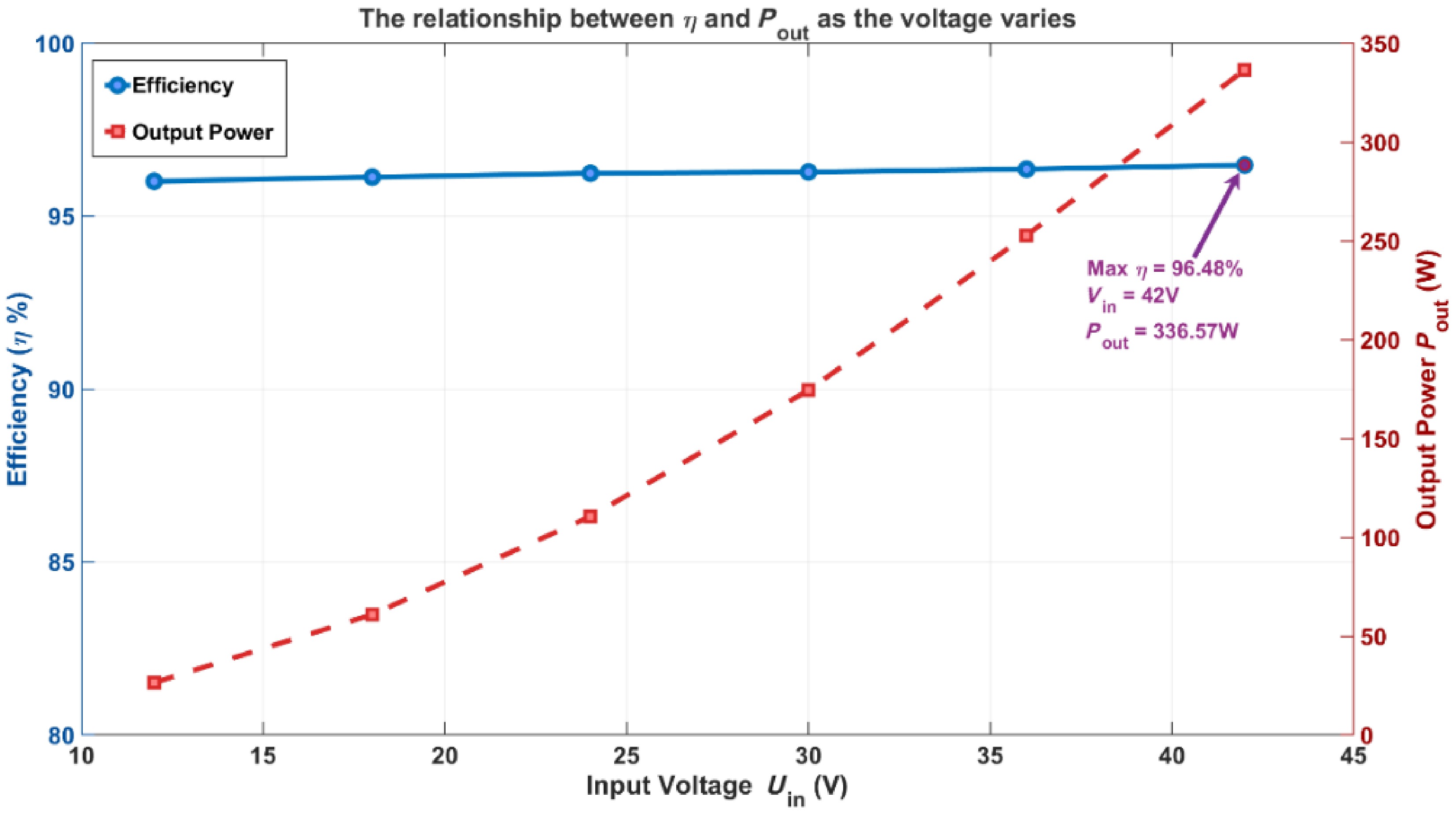
Figure 9.
Relationship between η and Pout when the Req is 5 Ω.
-
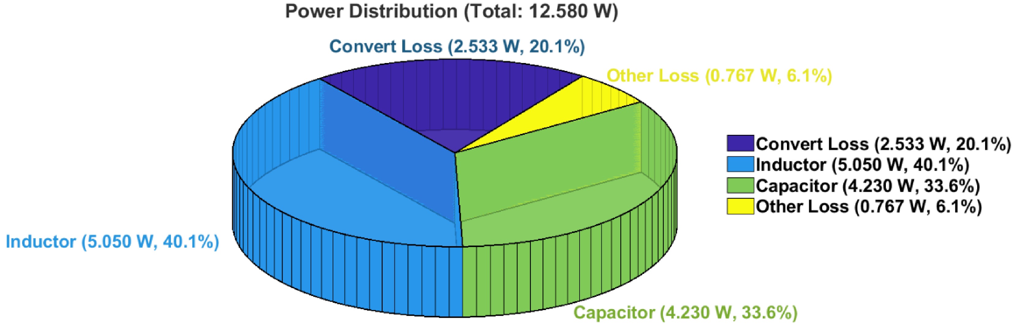
Figure 10.
Power loss distribution.
-
Parameters Symbol Value Input voltage Uin 12−48 V Primary inductance Lp 1.79 μH Primary resonant capacitor Cp 15.5 nF Primary internal resistances Rp 23 mΩ Coil spacing d 10 mm Coupling coefficient k 0.32 Load resistance RL 5 Ω Secondary inductance Ls 1.77 μH Secondary resonant capacitor Cs 13.5 nF Secondary internal resistances Rs 28 mΩ Switching frequency fSW 1 MHz GaN's output capacitance Qoss 50 nC Table 1.
System parameters.
-
ZVS boundary conditions Switching frequency (fSW) (MHz) φp = 0 0.9034 φs = 0 0.9582 XS = XS,max 1.0238 Network resonance: XS = 0 1.0242 Table 2.
The ZVS boundary conditions and network resonance.
-
Table 3.
Comparison with other works.
Figures
(10)
Tables
(3)