-
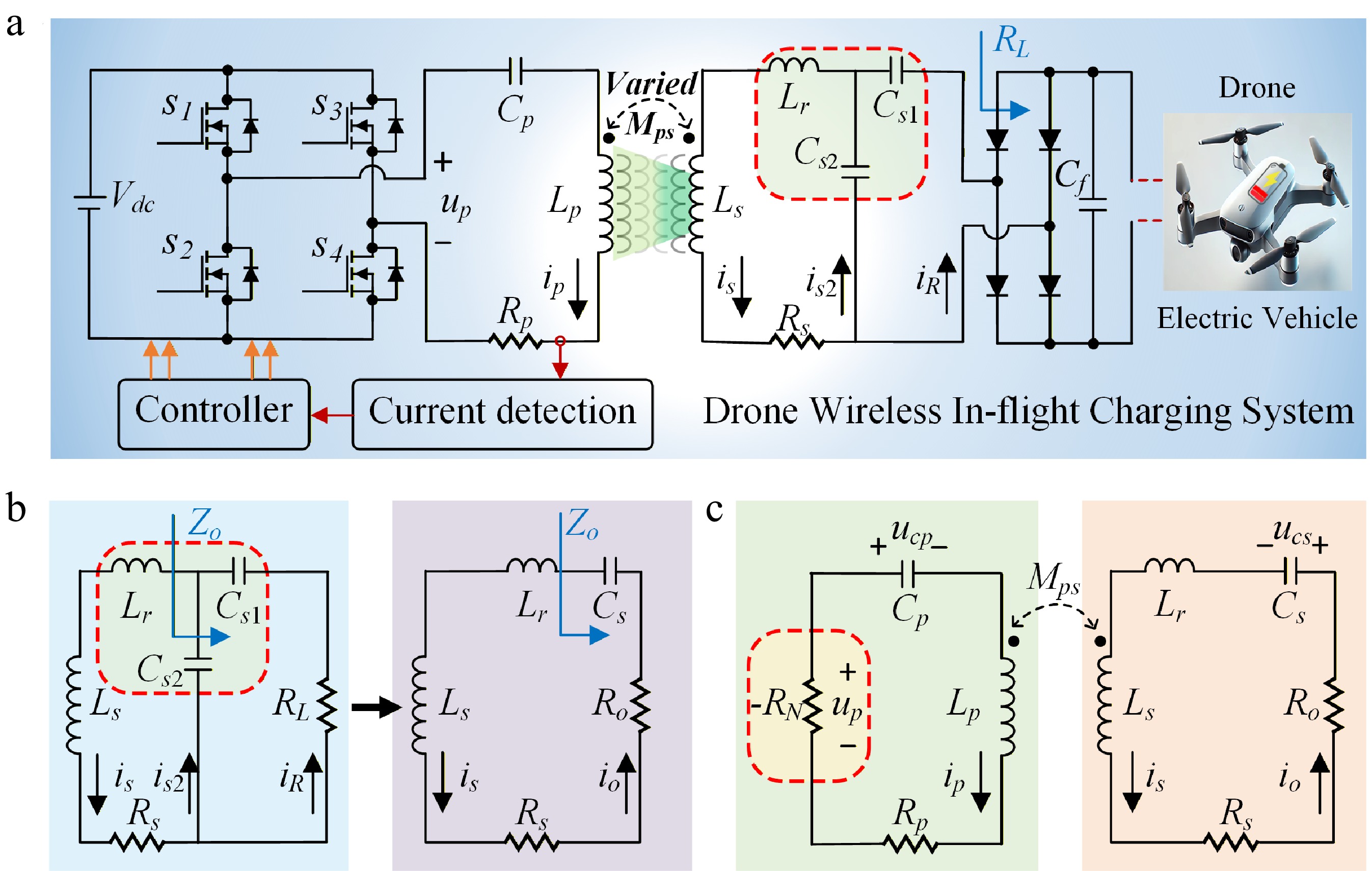
Figure 1.
Schematic of (a) the proposed drone wireless in-flight charging system. (b) Equivalent transformation of the SLDC topology. (c) Equivalent transformation of the system.
-
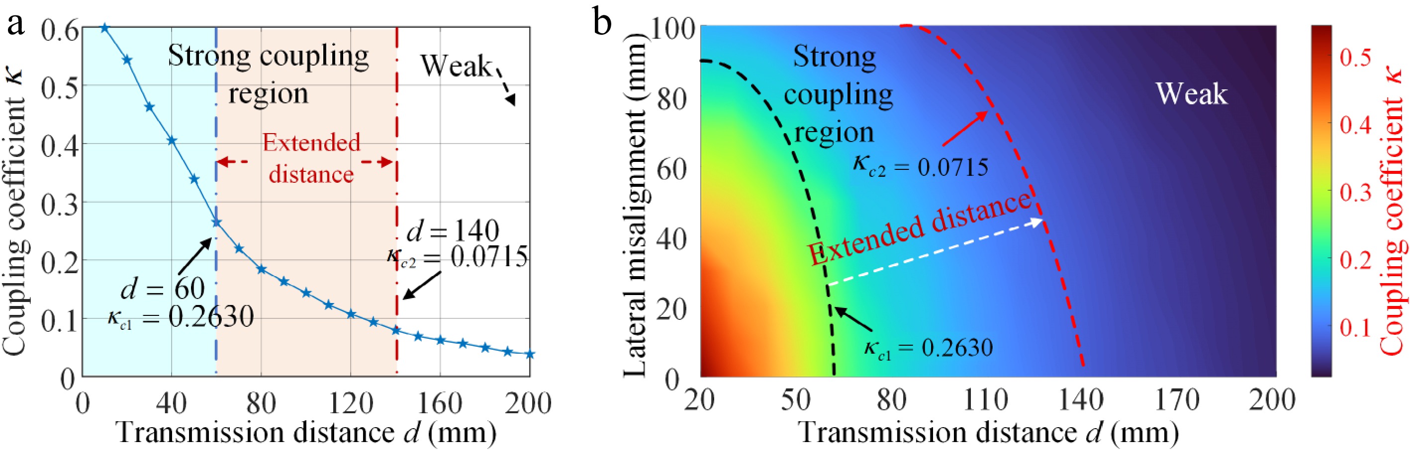
Figure 2.
(a) Effect of coupling coefficient κ on transmission distance. (b) Effect of κ on transmission distance and lateral misalignment.
-
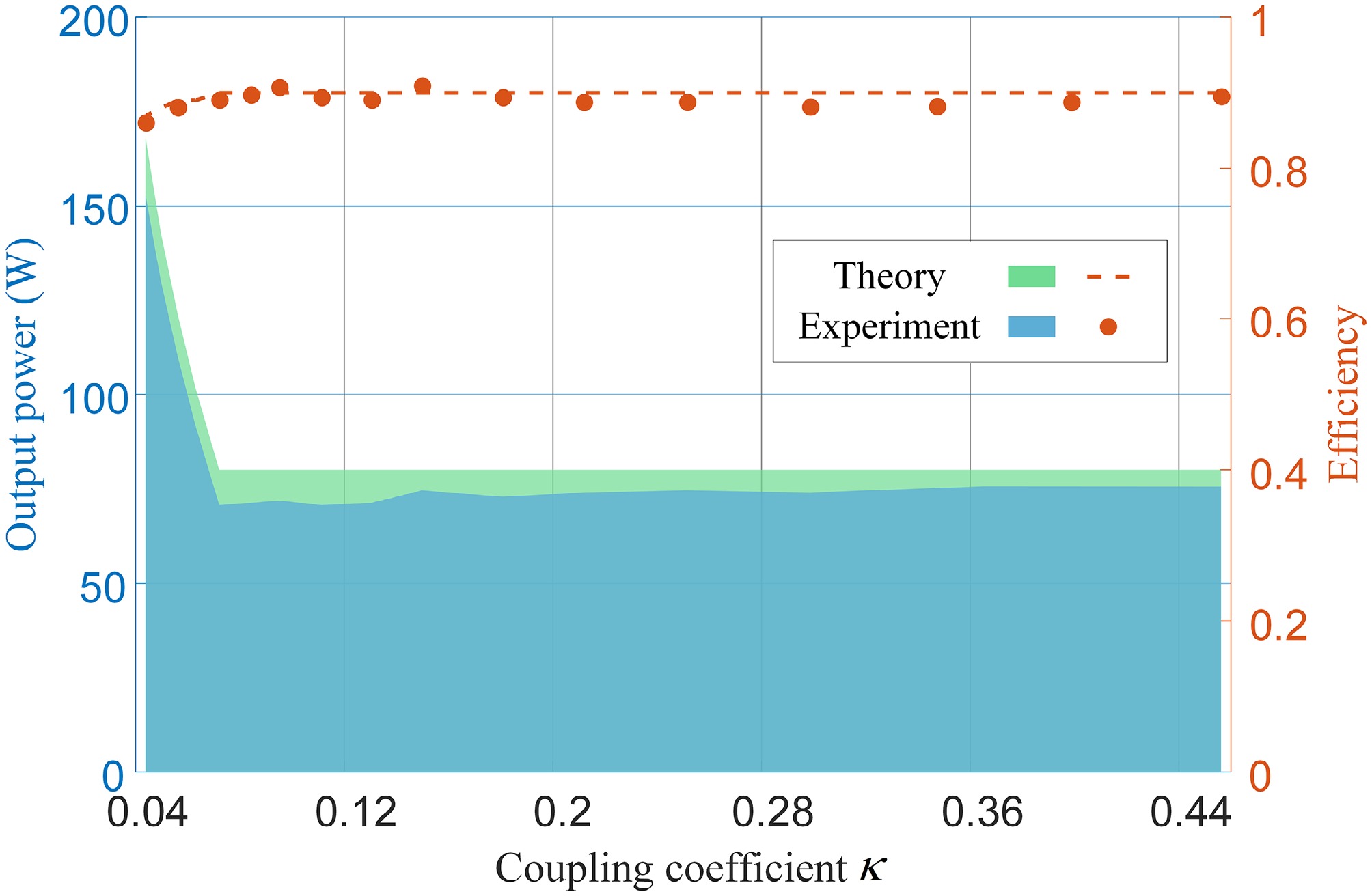
Figure 3.
Relationship between output power, transmission efficiency and coupling coefficient in the PT-WPT system.
-
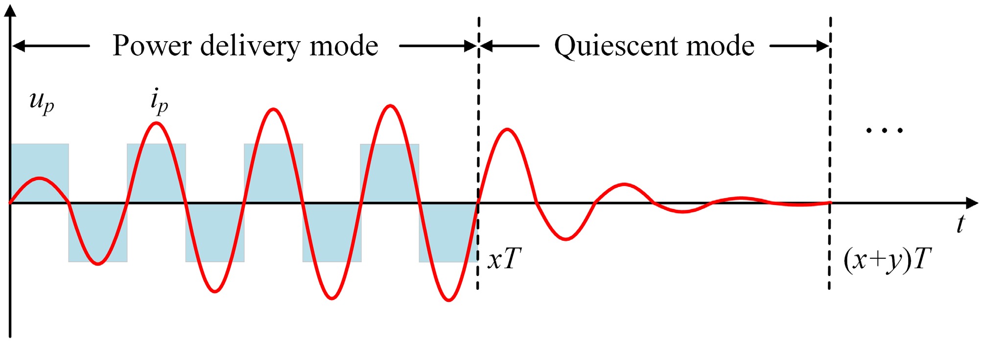
Figure 4.
Schematic diagram of PDM.
-
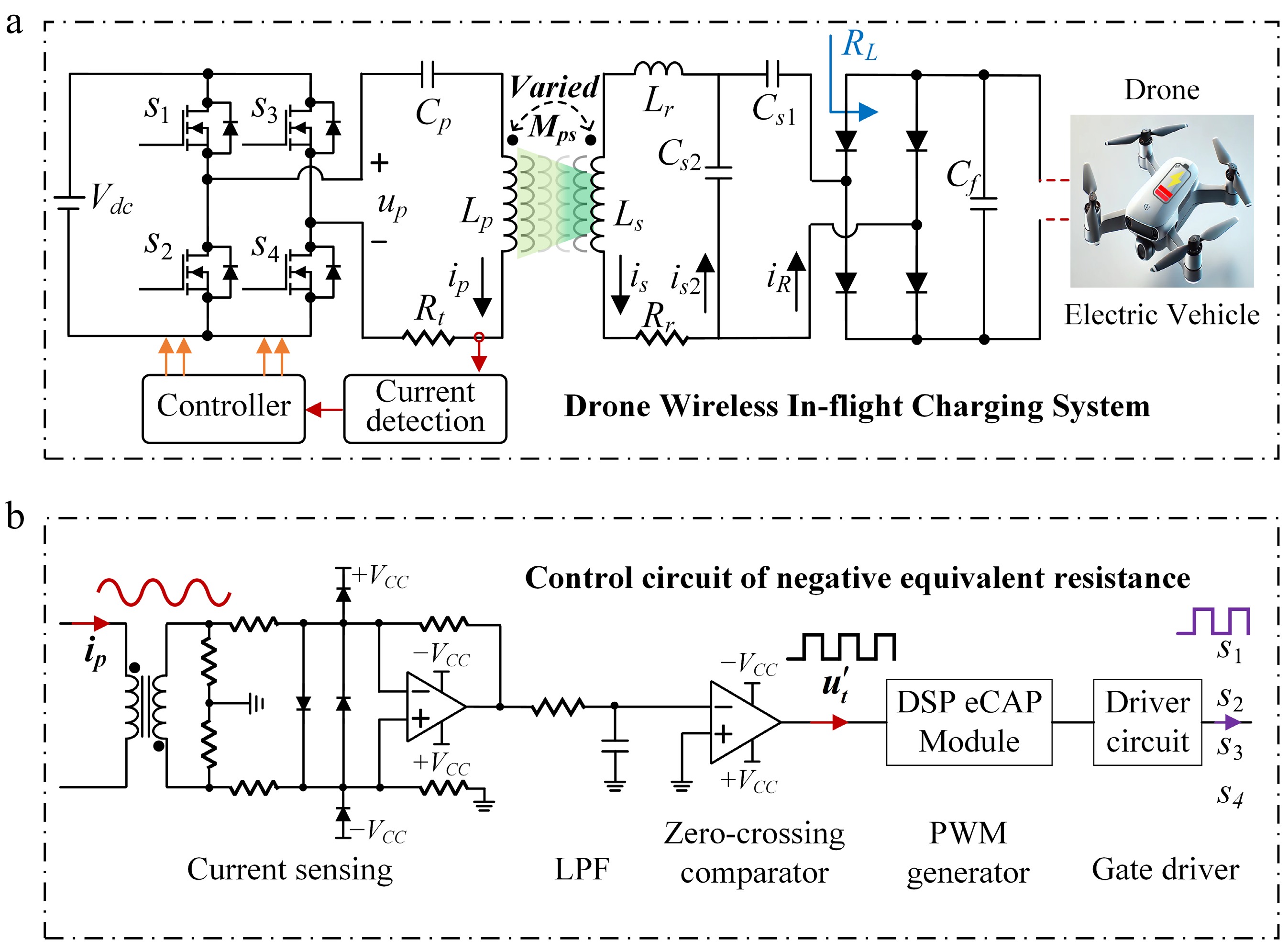
Figure 5.
Circuit design of the PT-WPT system employing APDM. (a) Power stage. (b) Block diagram of the controller.
-
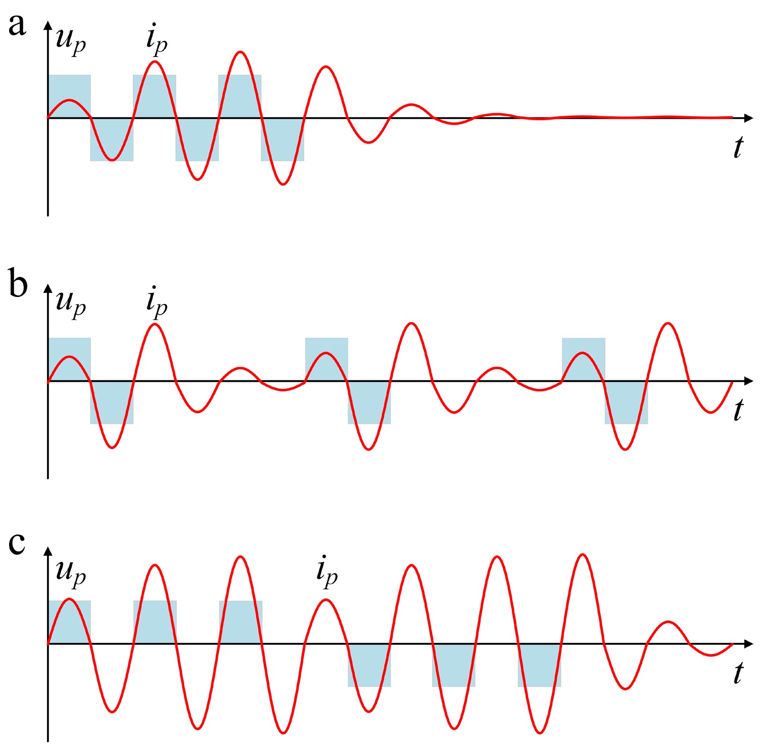
Figure 6.
Schematic diagrams of full-wave and half-wave PDM modulation. (a) Response under densely distributed full-wave PDM. (b) Response under uniformly distributed full-wave PDM. (c) Response under uniformly distributed half-wave PDM.
-
Figure 7.
Waveforms of inverter output voltage and current at N = 8 and m = 0.25.
-
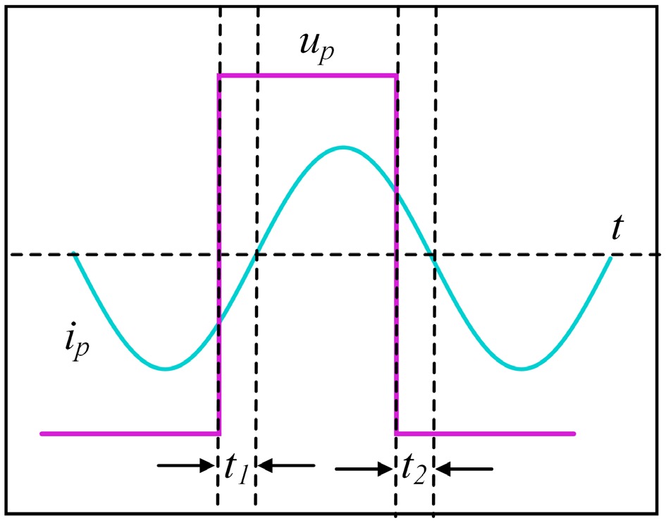
Figure 8.
Implementation process of ZVS.
-
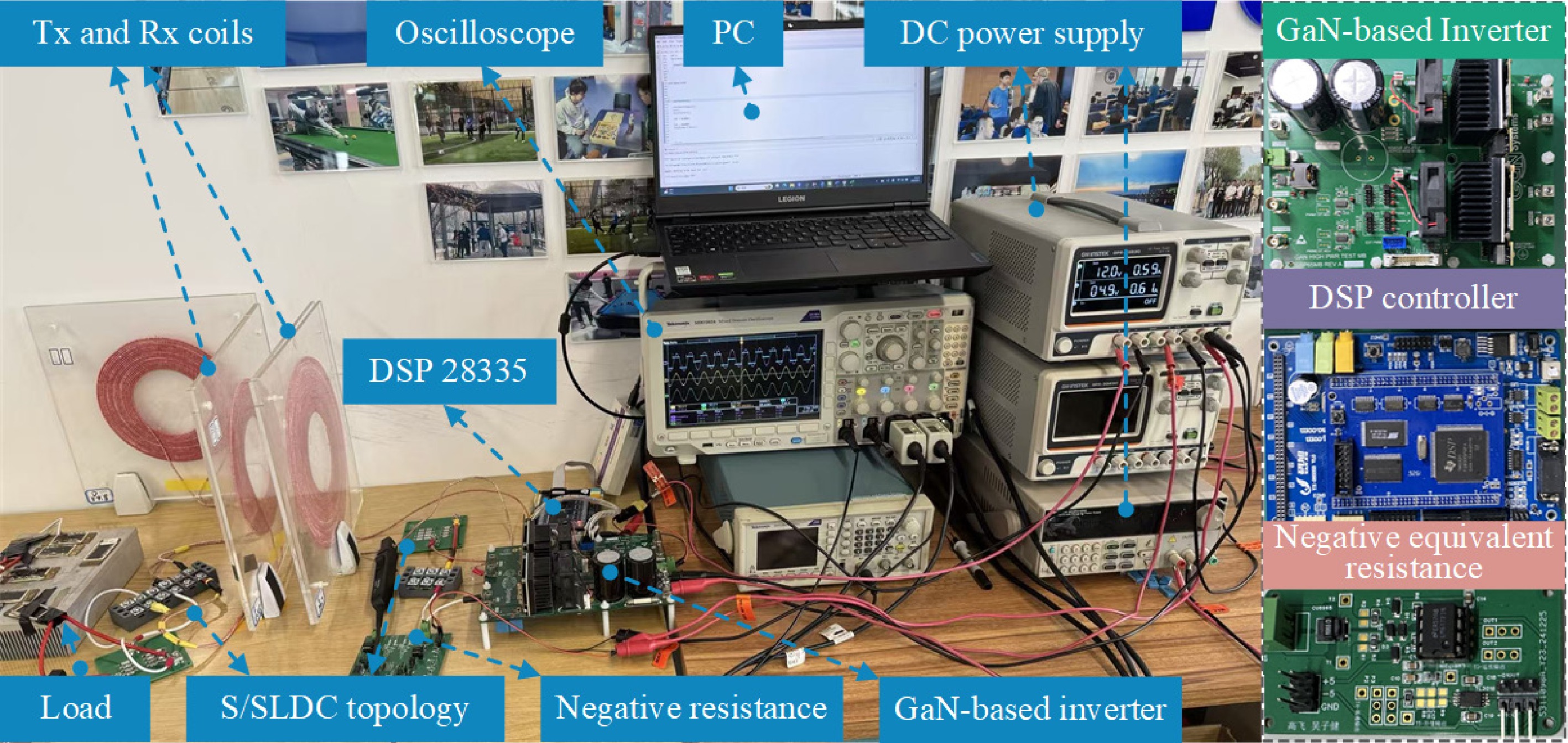
Figure 9.
Experimental prototype of the proposed S/SLDC higher-order PT-WPT system.
-
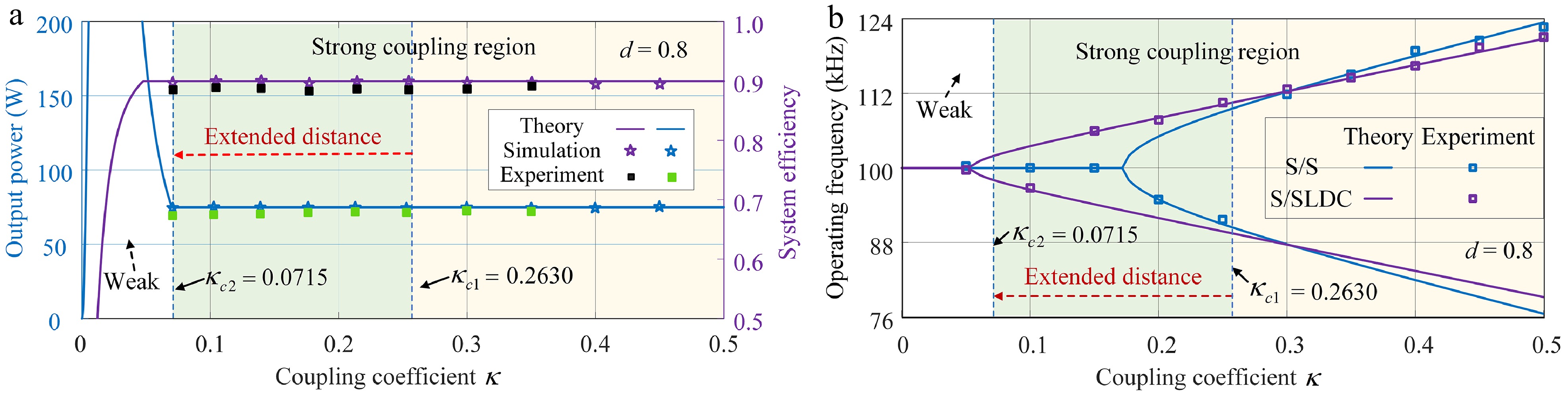
Figure 10.
Schematic diagram of output characteristics under m = 0.8. (a) Output power and transmission efficiency. (b) System operating frequency.
-
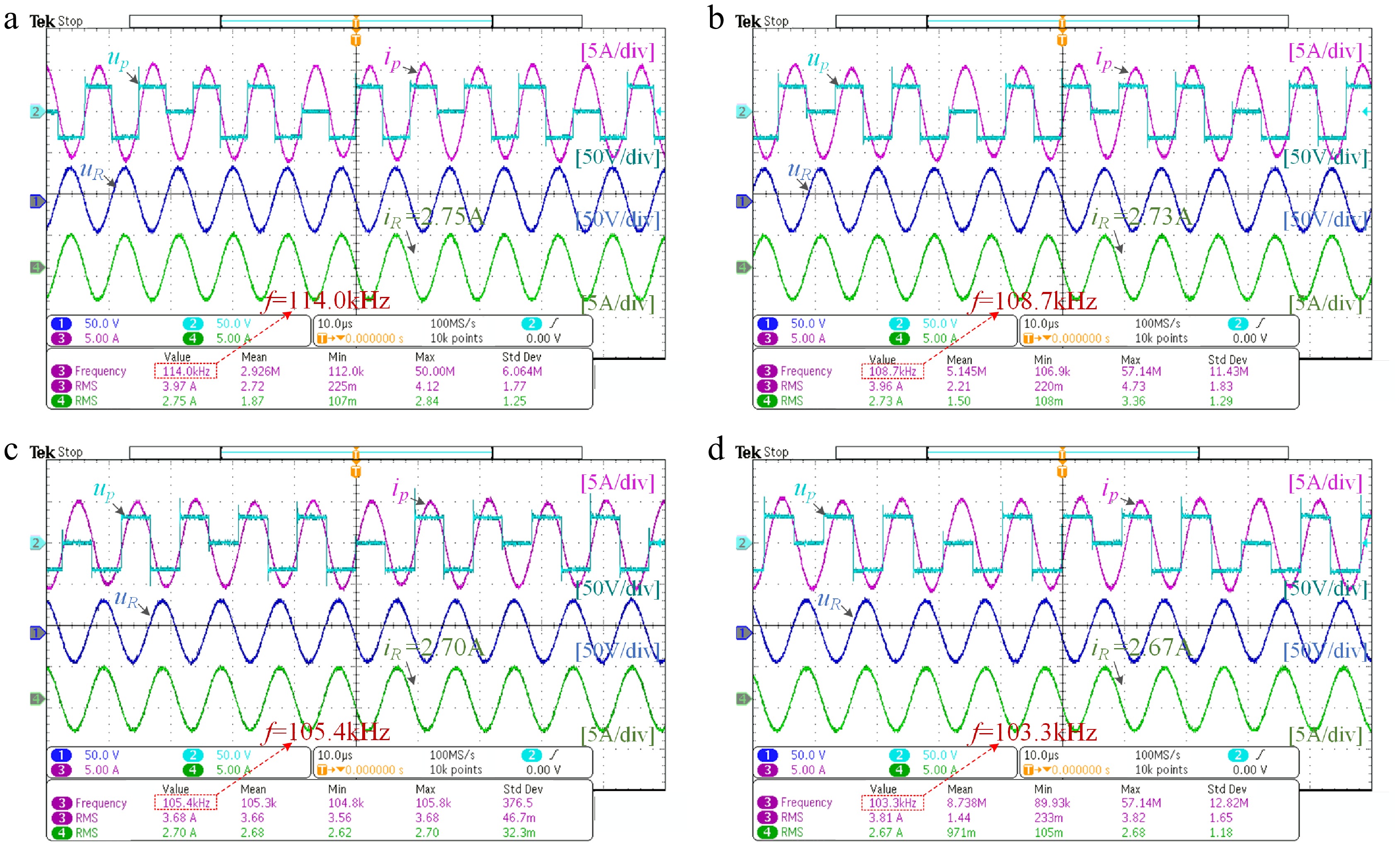
Figure 11.
Experimental waveforms at different transmission distances under m = 0.8. (a) d = 40 mm. (b) d = 60 mm. (c) d = 80 mm. (d) d = 100 mm.
-
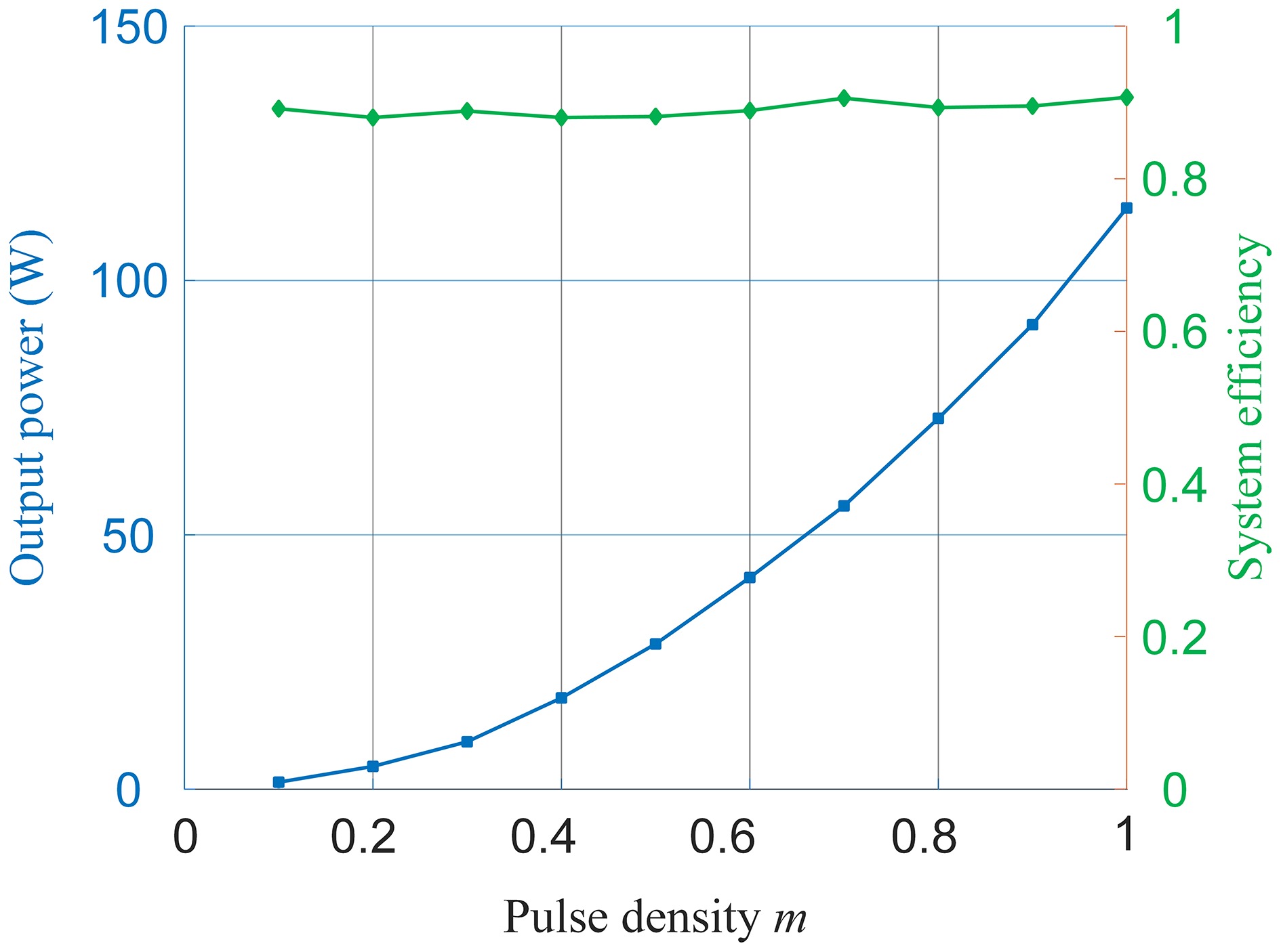
Figure 12.
Output power and efficiency under different pulse densities at 100 mm transmission distance.
-
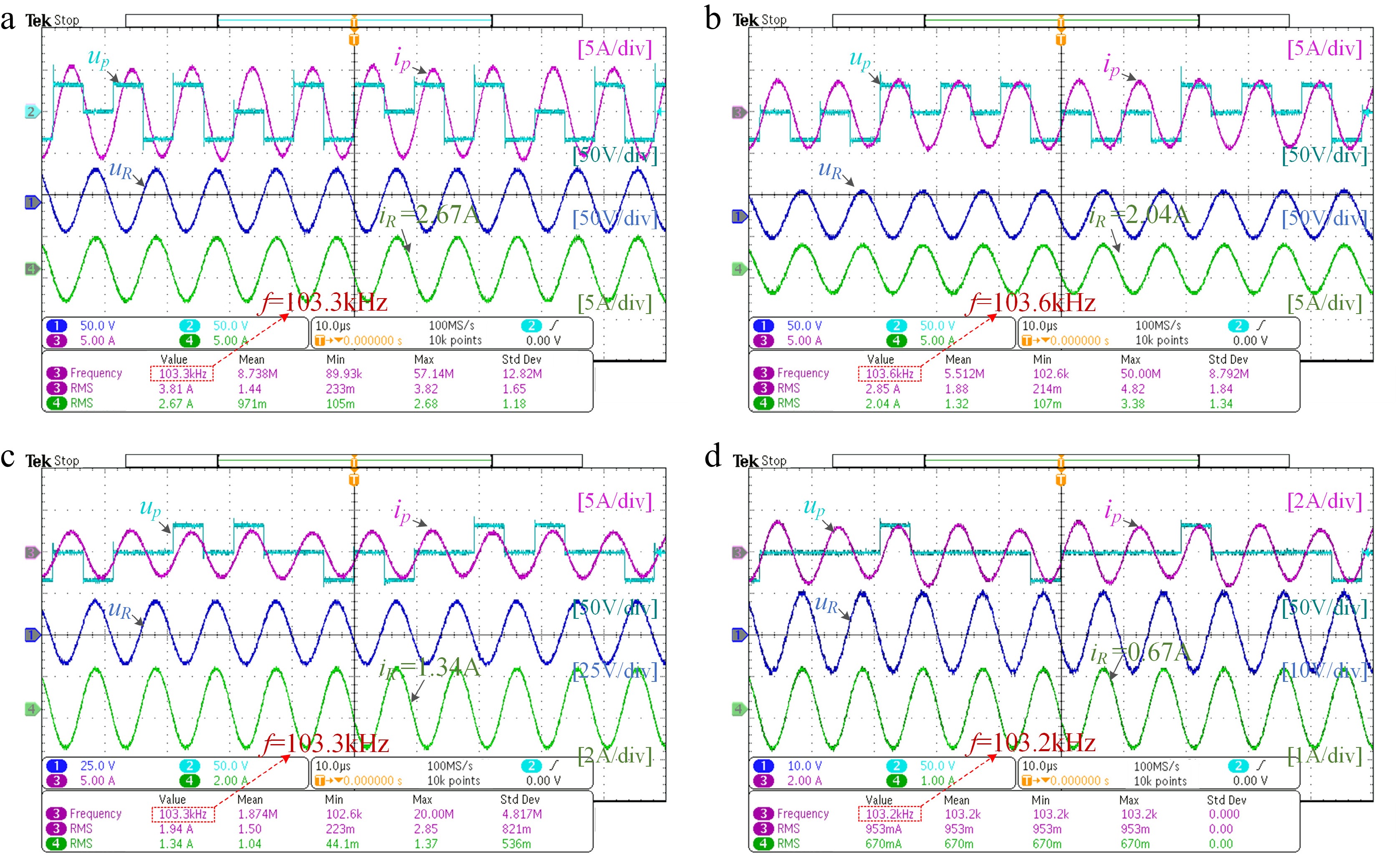
Figure 13.
Experimental waveforms under different pulse densities at 100 mm transmission distance. (a) m = 0.8. (b) m = 0.6. (c) m = 0.4. (d) m = 0.2.
-
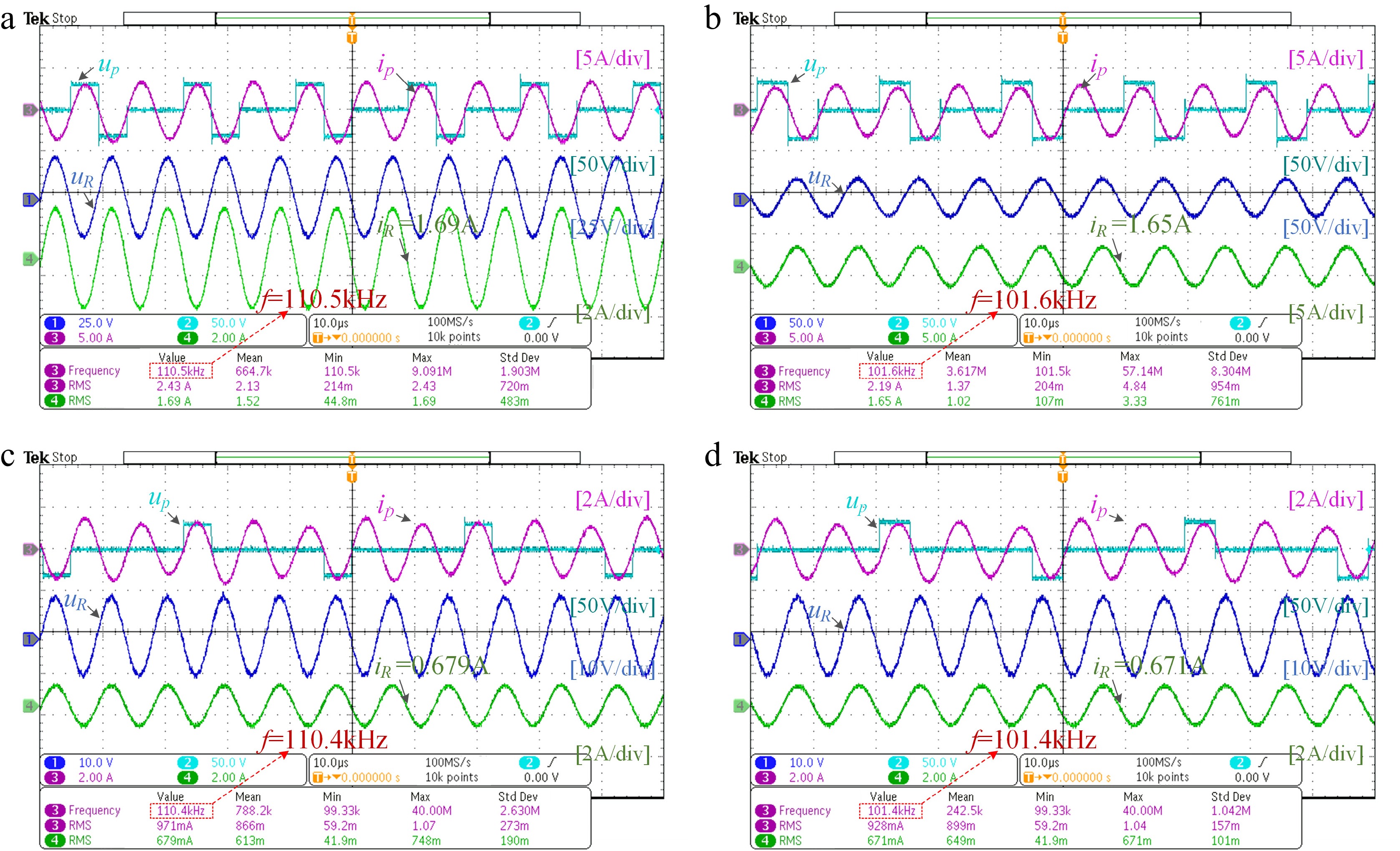
Figure 14.
Experimental waveforms at different distances and pulse densities. (a) m = 0.5, d = 50 mm. (b) m = 0.5, d = 120 mm. (c) m = 0.2, d = 50 mm. (d) m = 0.2, d = 120 mm.
-
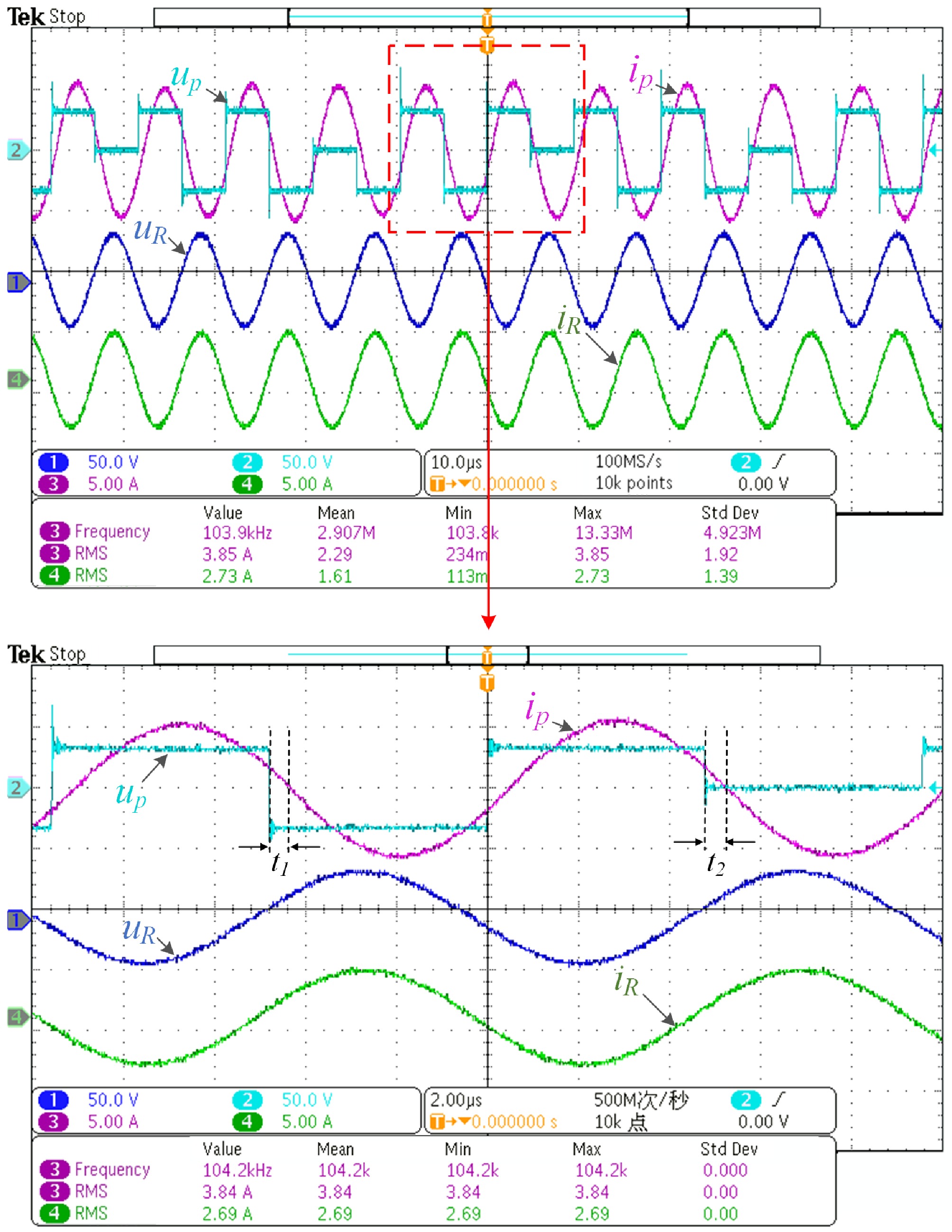
Figure 15.
ZVS implementation process at m = 0.8 and d = 90 mm.
-
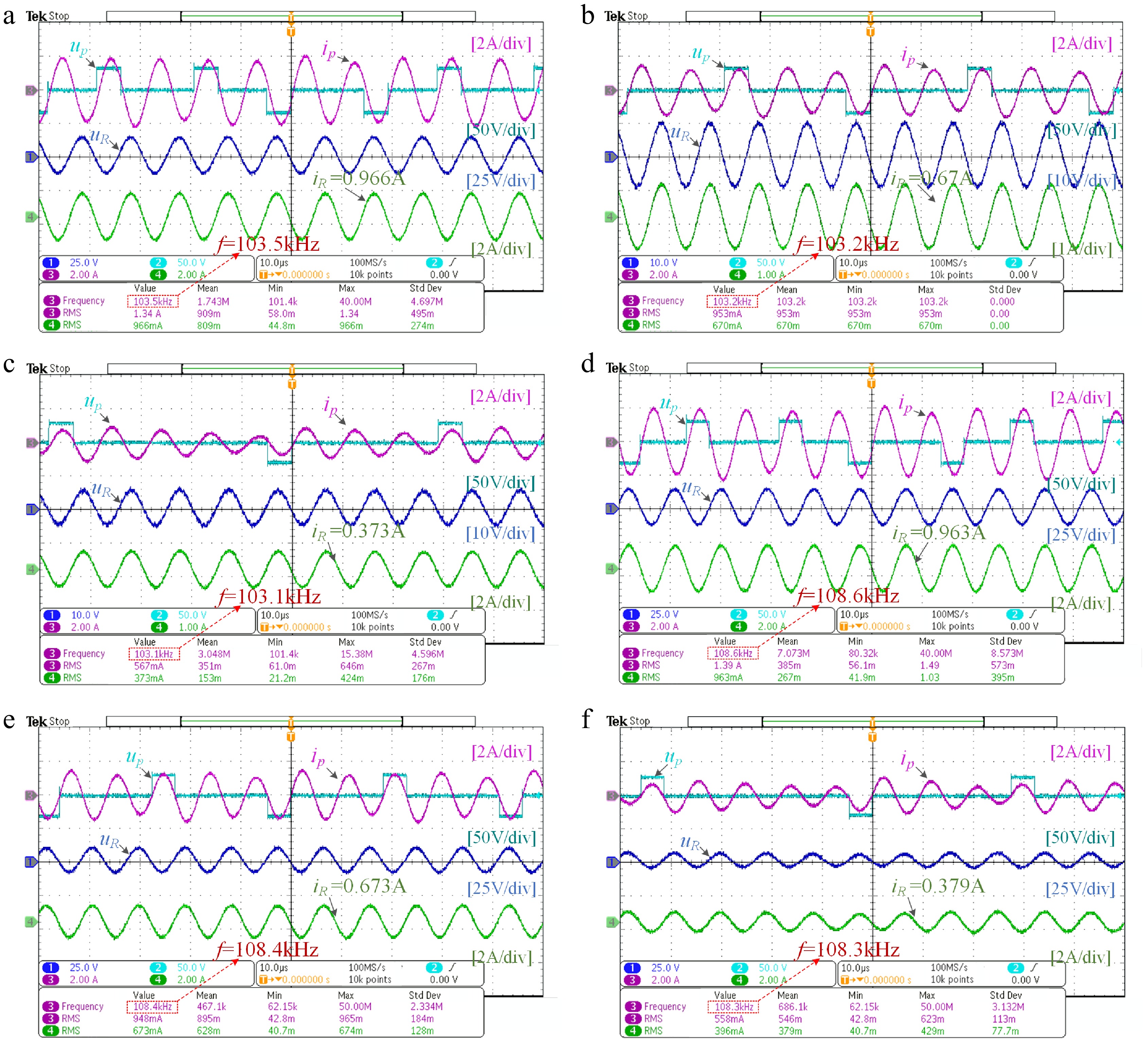
Figure 16.
Experimental waveform with low pulse density. (a) d =100 mm, m = 0.3. (b) d = 100 mm, m = 0.2. (c) d = 100 mm, m = 0.1. (d) d = 60 mm, m = 0.3. (e) d = 60 mm, m = 0.2. (f) d = 60 mm, m = 0.1.
-
N m Sw (N, m) 8 0.125 1000000−100000000 7 0.140 1000000−10000000 6 0.170 10000−1000000 5 0.200 10000−10000 4 0.250 100−10000 7 0.290 1000100−1000−100 3 0.330 100−100 8 0.375 100−10010100−10−100 5 0.400 100−10−10010 7 0.430 1010100−10−10−100 2 0.500 1−100 7 0.570 1010101−10−10−10−1 5 0.600 10101−10−10−1 8 0.625 101−10−1101−10−10−110 3 0.670 101−10−1 7 0.710 1−1101−10−11−10−110 4 0.750 1−1101−10−1 5 0.800 1−1101−11−10−1 6 0.830 1−1101−11−10−11−1 7 0.860 1−11−1101−11−10−1 8 0.875 1−11−11−1101−11−11−10−1 1 1.000 1−1 Table 1.
Switching sequences of the apdm with different N and m values.
-
Item Value Inductance of transmitting coil (Lp) 140.1 μH Resistance of primary side (Rp) 0.4 Ω Capacitance of primary side (Cp) 18.08 nF Inductance of pickup coil (Ls) 60.39 μH Inductance of added inductor (Lr) 59.62 μH Capacitance of series capacitor (Cs1) 12.664 nF Capacitance of parallel capacitor (Cs2) 8.4427 nF Resistance of secondary side (Rs) 0.3 Ω Resistance of load (RL) 10 Ω System natural operating frequency (f0) 100 kHz Table 2.
Key parameters of prototype.
-
Ref. Scheme PT-symmetry maintained? Power regulation? High system flexibility ZVS Frequency (kHz) Output power (W) Transfer efficiency [14] PWM Yes No Good No 100 75 87.5% [19] DC-DC No Yes Unexpected No 85 1 − [20] PFM Yes Yes Unexpected Yes 200 41.8 86.4% [23] PDM No Yes Unexpected Yes 85 787.5 80%–93.3% [27] PWM Yes No Unexpected No 200 50 90.8% This paper APDM Yes Yes Good Yes 100 112 88% Table 3.
Comparative analysis between the proposed system and others.
Figures
(16)
Tables
(3)