-
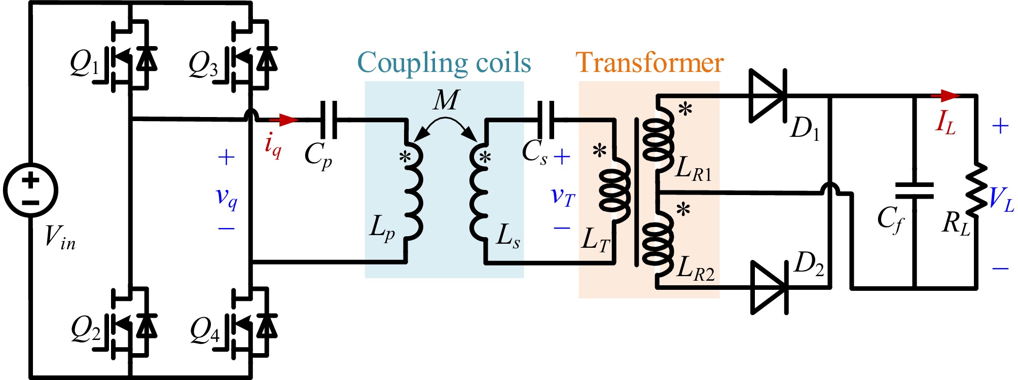
Figure 1.
The proposed S/S compensated WPT system utilizing full-wave rectification.
-
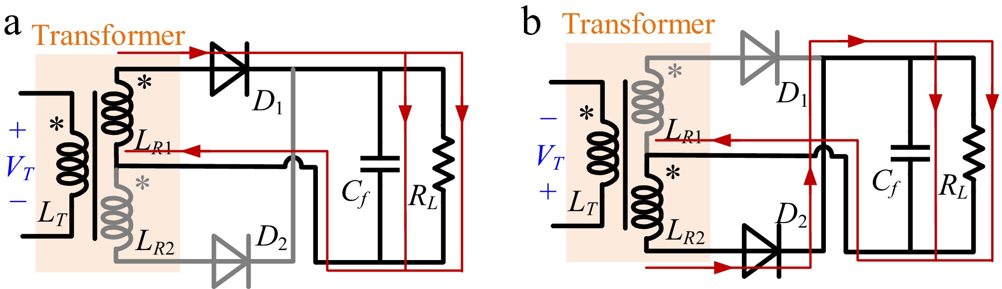
Figure 2.
Operating states of full-wave rectifier (a) State I. (b) State II.
-
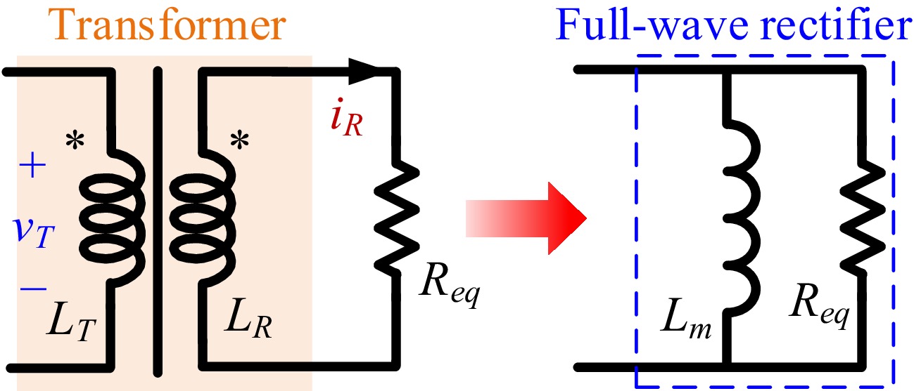
Figure 3.
Equivalent circuit of employed full-wave rectifier.
-
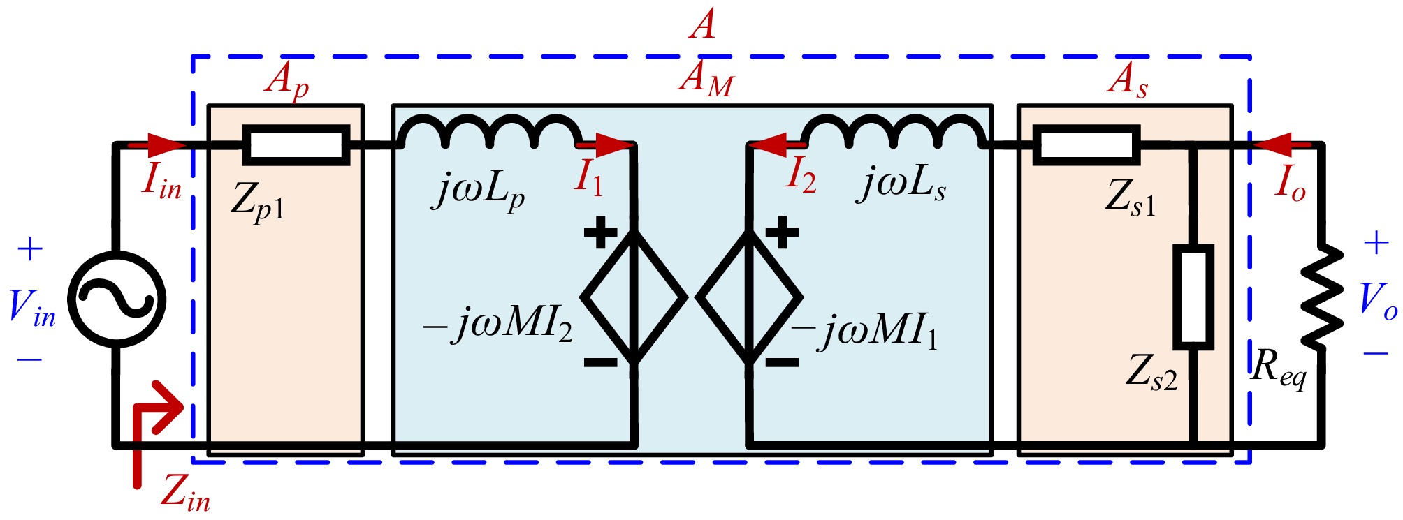
Figure 4.
Equivalent S/SP resonance circuit.
-
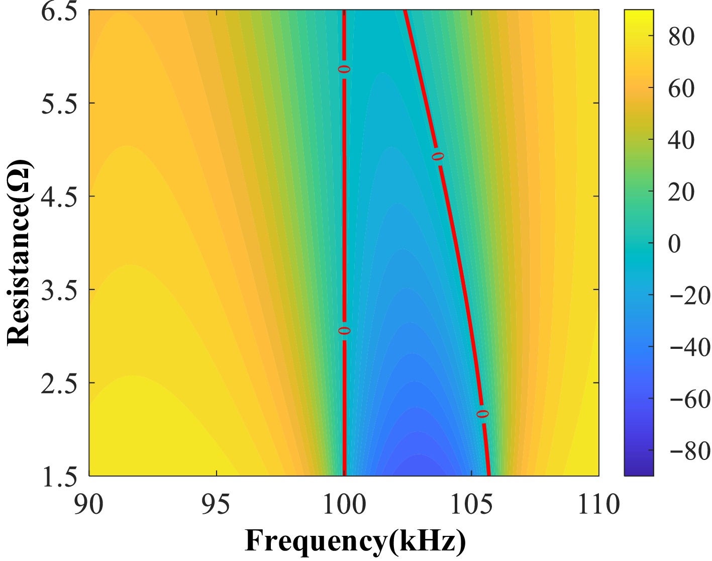
Figure 5.
Equivalent impedance angle (degrees) at varying loads and frequencies.
-
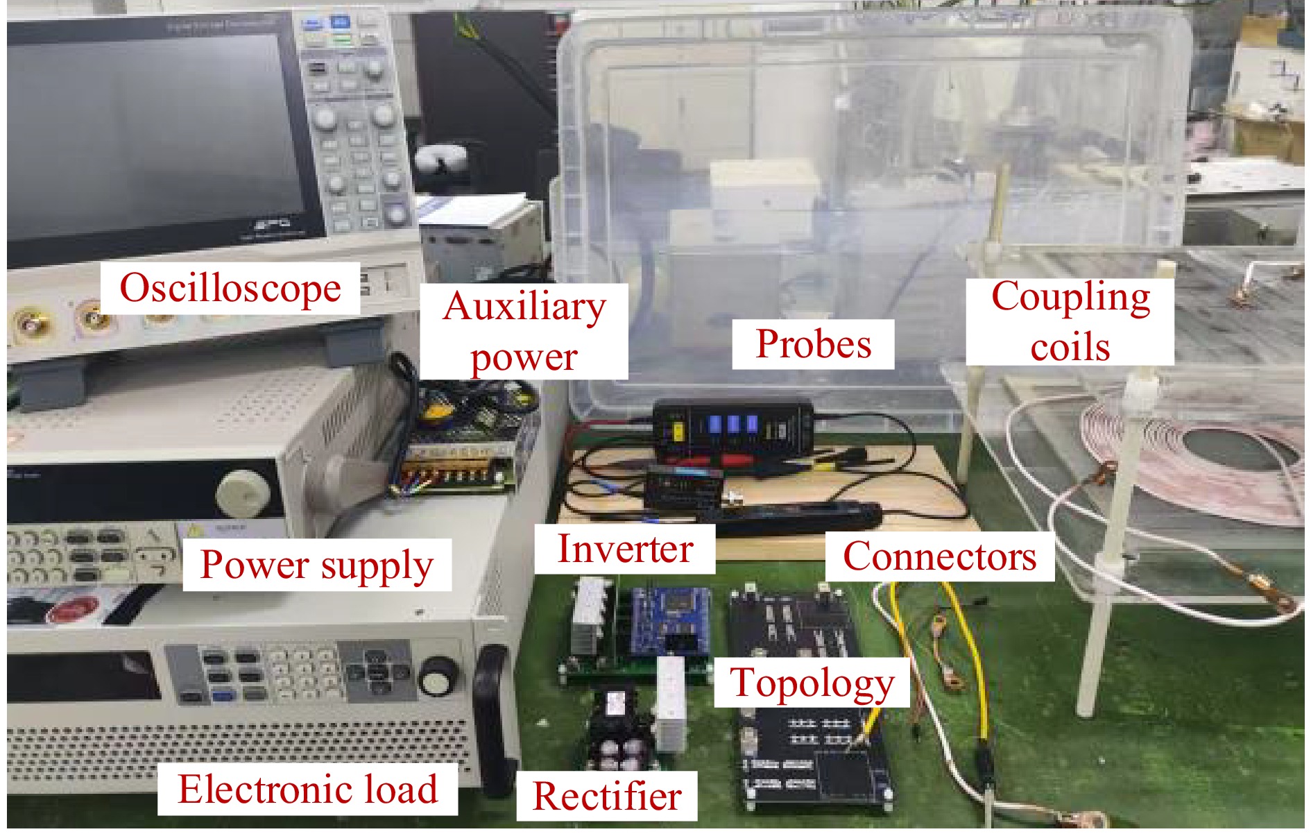
Figure 6.
Experimental prototype setup.
-
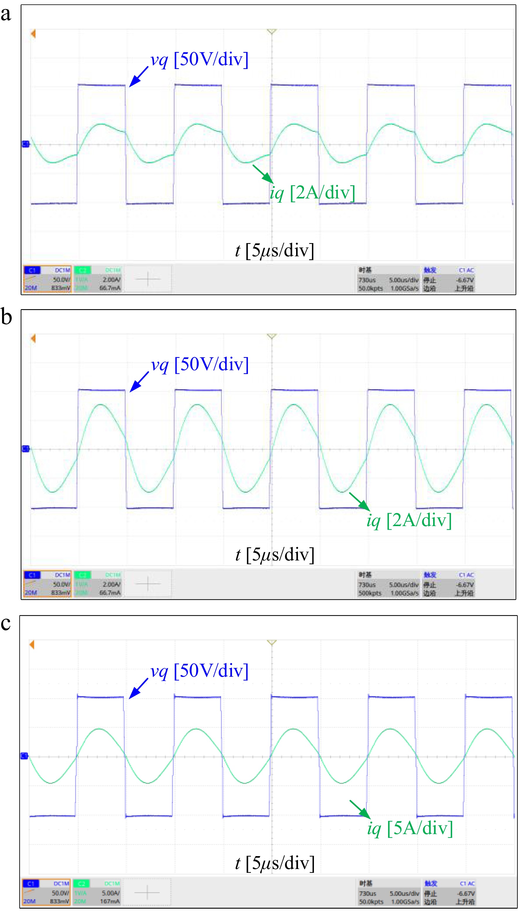
Figure 7.
The inverter output waveforms with different loads. (a) RL = 2-Ω. (b) RL = 5-Ω. (c) RL = 8-Ω.
-
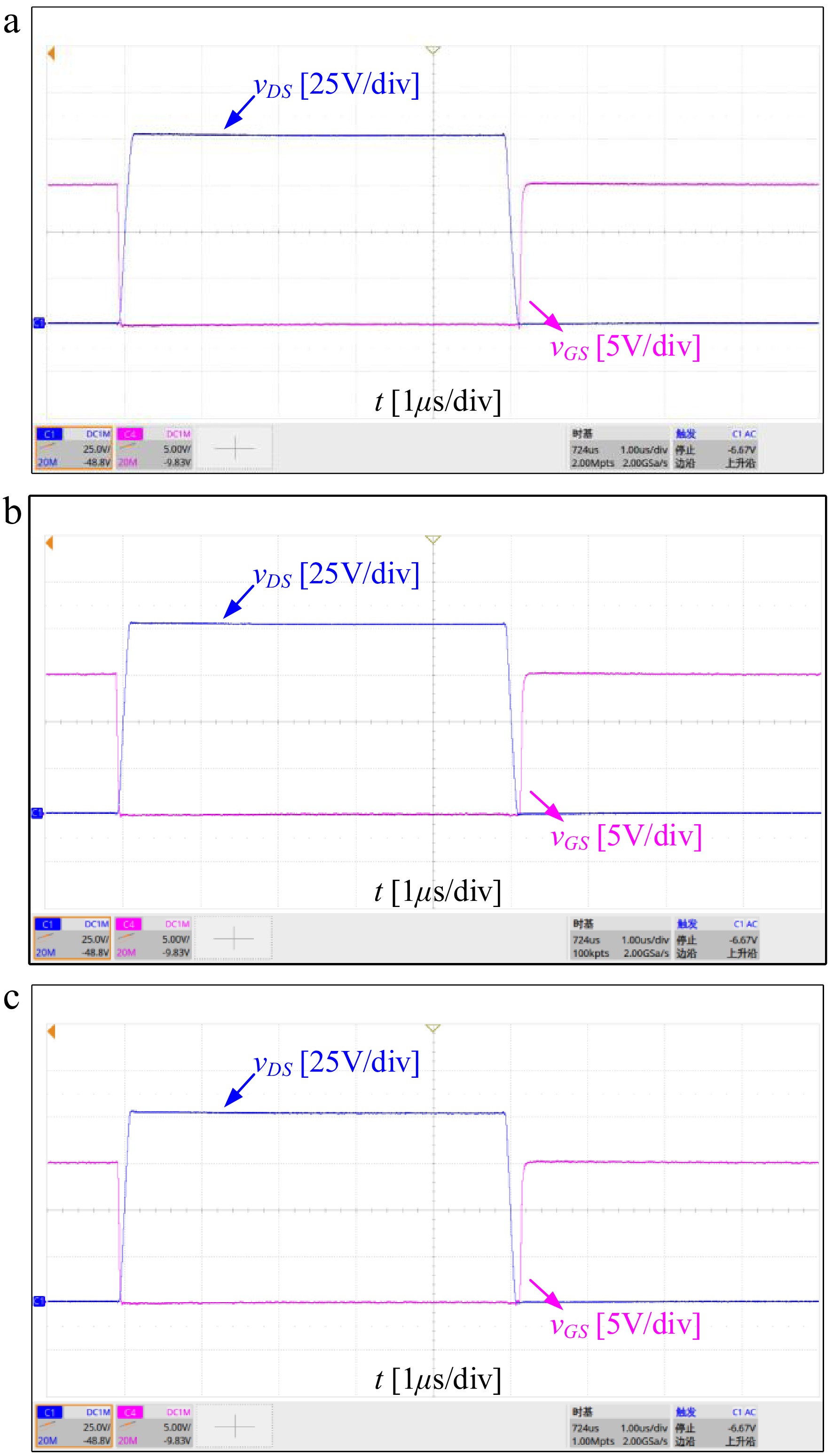
Figure 8.
VDS and VGS of inverter MOSFETs with different loads. (a) RL = 2-Ω. (b) RL = 5-Ω. (c) RL = 8-Ω.
-
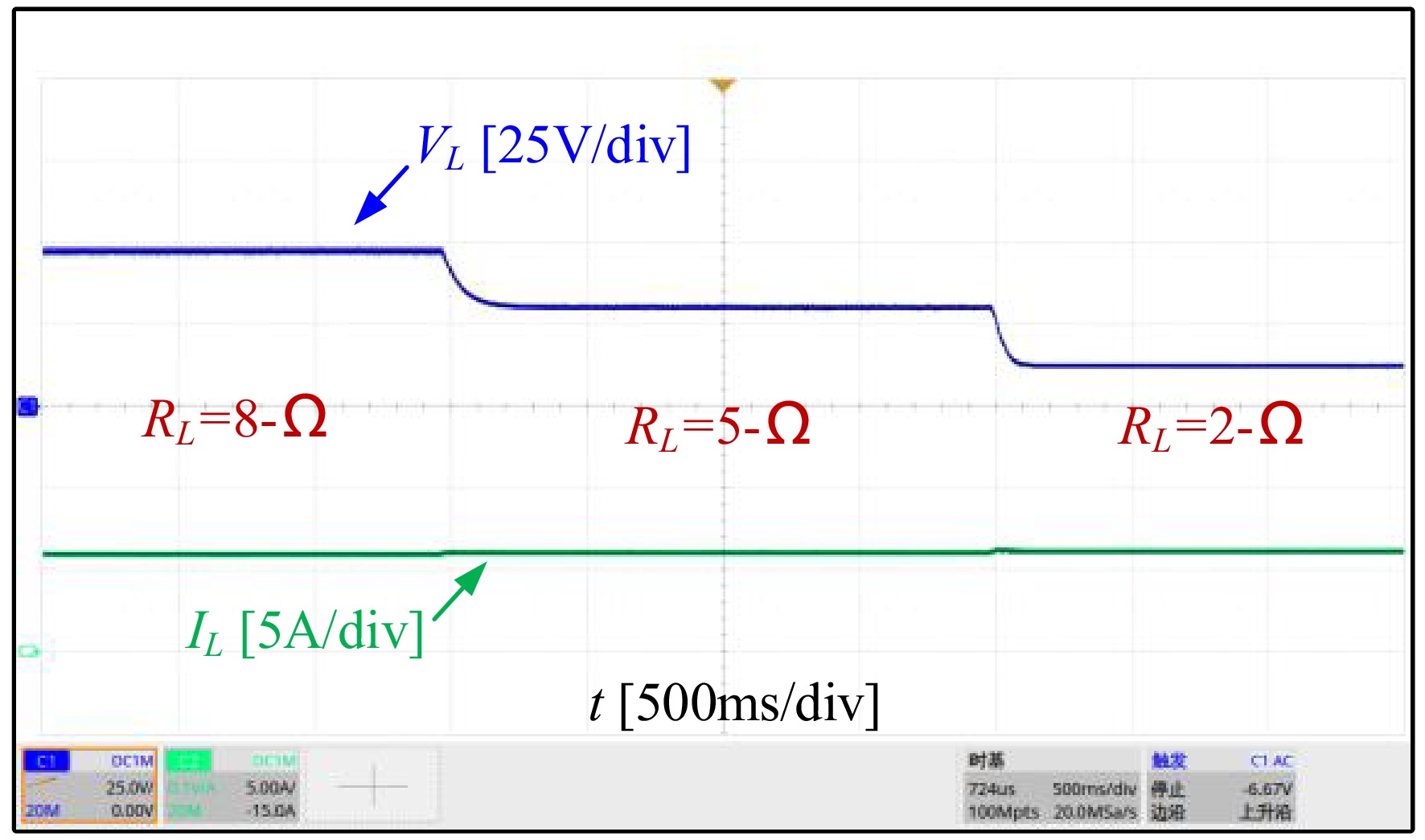
Figure 9.
Transient behaviors with step load.
-
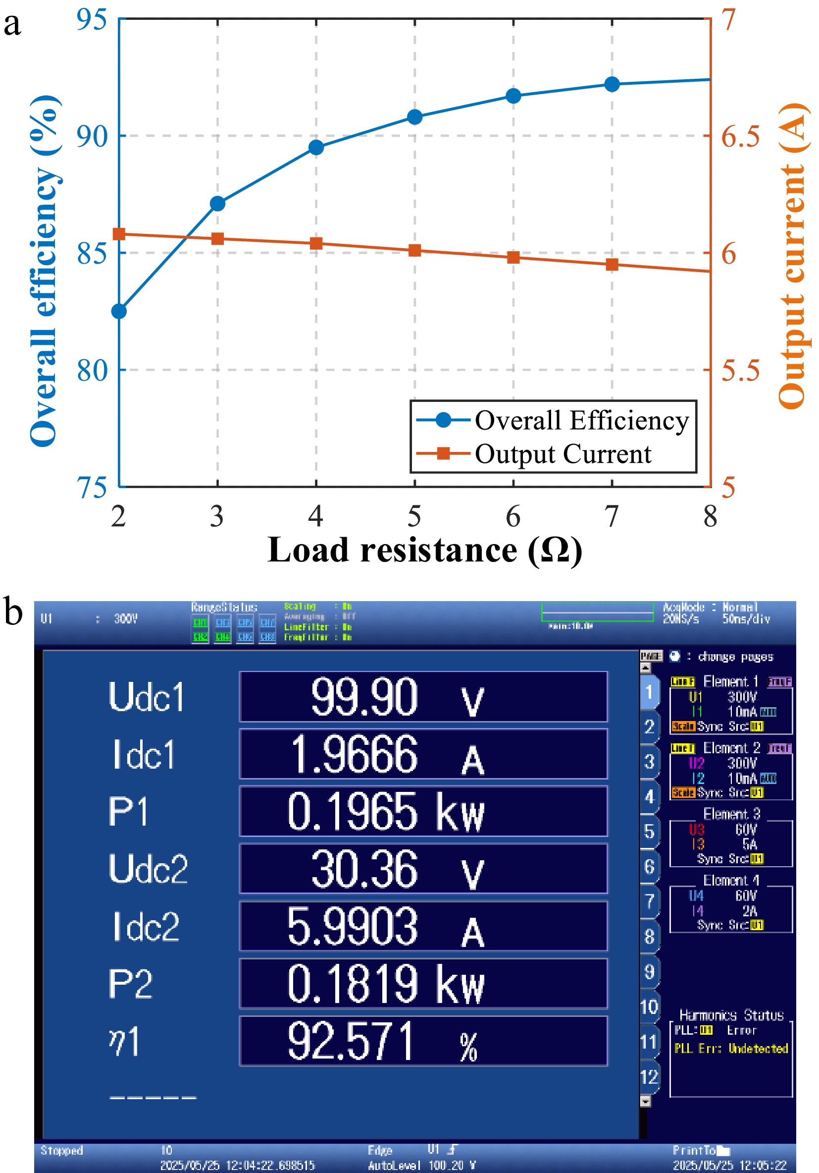
Figure 10.
System efficiency performance. (a) Overall efficiency with different loads. (b) The overall efficiency at rated load.
-
Part Value Part Value f 100 kHz Req 1.5–6.5 Ω Cp 25.3 nF Lp 120 μH Cs 21.1 nF Ls 120 μH M 20 μH Lc 20 μH Table 1.
A parameter combination following the proposed design methodology.
-
Part Value Part Value Vin 100 V ω 200π rad/s Cp 25.5 nF Lp 120.8 μH Cs 21.2 nF Ls 119.6 μH M 21.5 μH Lm 21.5 μH Cf 200 μF RL 2–8 Ω Table 2.
System parameters setup.
Figures
(10)
Tables
(2)