


-
Wireless power transfer (WPT) has emerged as a highly convenient and transformative technology that enables the transmission of electrical energy without physical contact. This inherent non-contact capability positions WPT with significant application prospects across a diverse range of fields, including but not limited to electric vehicles, consumer electronics, biomedicine, and various industrial sectors[1−6].
In wireless charging applications, constant current (CC) charging constitutes the predominant operational phase, which necessitates that the WPT system maintains a stable CC output across a specified range of load conditions[7,8]. Commonly employed CC output compensation topologies include S/S[9−11] and LCC/LCC[12−14] compensation. The LCC/LCC topology, classified as a compound high-order compensation topology, offers advantages in both safety and stability. However, the numerous resonant components lead to significant loop losses, which inherently limit improvements in system conversion efficiency. Conversely, the S/S compensation topology boasts a simpler structure and higher conversion efficiency. Nevertheless, under open-loop conditions, the transmitter enters a short-circuit state upon load removal, compromising safety. While methods to compensate for leakage inductance in the transmitter can prevent the system from entering a short-circuit state, with the introduction of only one additional compensation component. An S/SP topology is proposed based on compensating for the leakage inductance of coupling coils, achieving zero phase angle (ZPA) while avoiding potential dangers under no-load conditions[15]. Building upon this work, scholars optimized the compensation parameters and proposed an anti-offset S/SP compensated topology, achieving low output fluctuation under wide load and coupling ranges[16]. Nevertheless, all these studies concentrate on constant voltage output, and a CC output topology with leakage inductance compensation has not yet been investigated. Consequently, it is meaningful to explore a novel topology based on partial compensation of coil self-inductances that can achieve high safety, high efficiency, and CC output under open-loop conditions.
In WPT receivers, to maximize output capability, a full-bridge rectifier or a full-wave rectifier is typically chosen as the AC-DC conversion device. When a full-bridge rectifier is applied, two rectifier diodes are connected in series in the circuit at the same time, leading to higher voltage drop and power loss[17]. When a full-wave rectifier is applied, only one rectifier diode operates at any given moment, resulting in lower voltage drop and power loss. However, the magnetizing inductance of the center-tapped transformer in a full-wave rectification structure can disrupt ZPA operation. Therefore, this paper argues that proposing a novel structure integrating the magnetizing inductance of the center-tapped transformer from the full-wave rectifier into the resonant network is significant.
To summarize, this paper proposes a reuse design method for a CC output WPT system using an S/S compensated full-wave rectifier structure. The main contributions of this paper include: (1) a novel CC output S/SP compensation structure that achieves both high efficiency and safety, as well as offering significant design flexibility; (2) a multiplexing method that incorporates the transformer magnetizing inductance from the full-wave rectifier structure into the resonant network, achieving theoretical ZPA and practical inverter soft-switching operation.
-
This section provides a detailed derivation of the resonant relationships for the S/SP CC output compensation topology, which compensates for the partial self-inductances of the coupling coils.
Concurrently, it explores the design principles of the proposed S/S compensated WPT system, which utilizes the magnetizing inductance of the full-wave rectifier transformer for dual functionality.
System overview
-
The proposed S/S compensated CC output WPT system is shown in Fig. 1. The system consists of a cascaded inverter, coupling coils with their series compensation topology, and a full-wave rectifier, ultimately outputting a constant DC current IL within a specified load range. The full-wave rectifier structure employed utilizes a 1:1:1 center-tapped tightly coupled transformer, and the magnetizing inductance effect cannot be negligible.
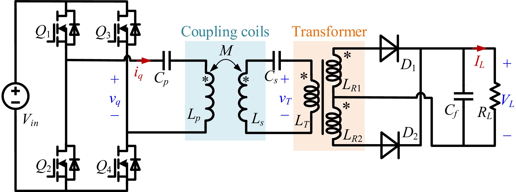
Figure 1.
The proposed S/S compensated WPT system utilizing full-wave rectification.
Full-wave rectifier modeling
-
The full-wave rectifier configuration employing a center-tapped transformer exhibits two operational states within a single period:
State I: As depicted in Fig. 2a, with a positive transformer input voltage, current flows from the LR1 winding to the load. Based on the dot convention of the transformer, the LR2 winding remains in a cutoff state due to the diode's unidirectional nature.
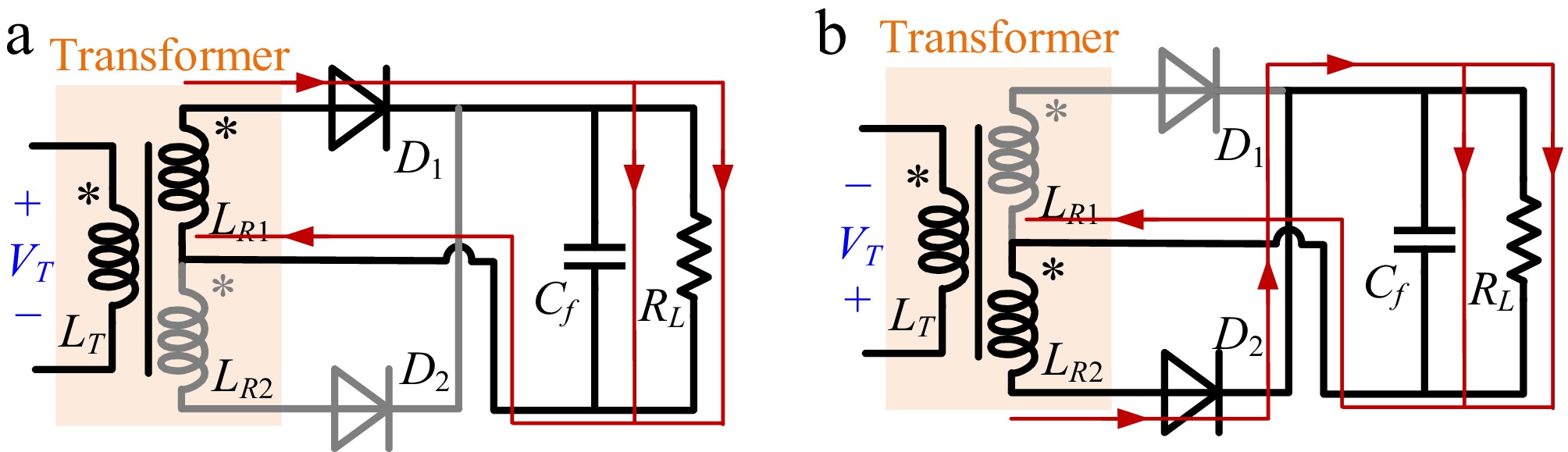
Figure 2.
Operating states of full-wave rectifier (a) State I. (b) State II.
State II: As depicted in Fig. 2b, with a negative transformer input voltage, current flows from the LR2 winding to the load. Based on the dot convention of the transformer, the LR1 winding remains in a cutoff state due to the diode's unidirectional nature.
The modal analysis reveals that the full-wave rectifier structure with a center-tapped transformer can be equivalently modeled as a 1:1 tightly coupled transformer driving a resistive load. As illustrated in Fig. 3, the secondary winding LR satisfies the relationship presented below:
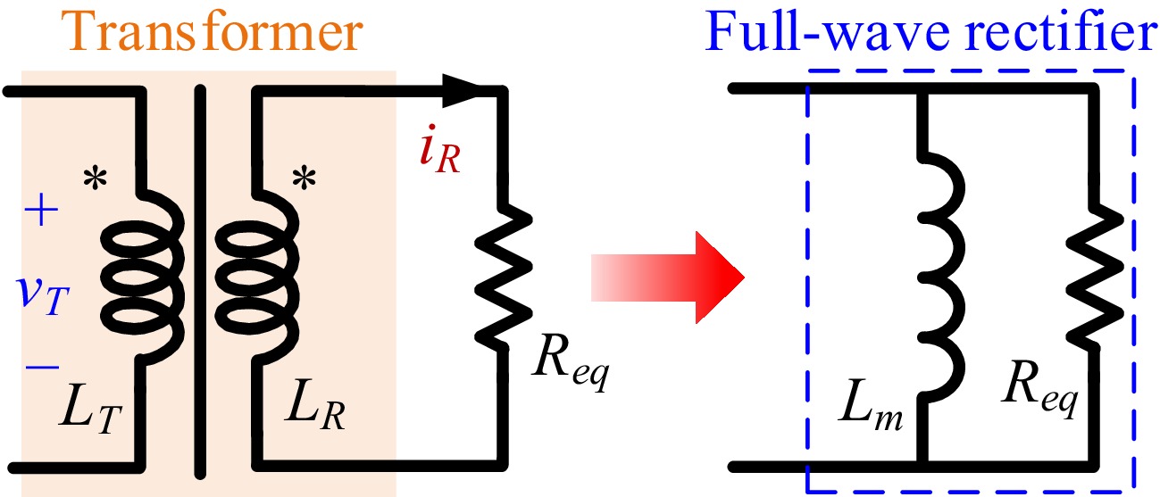
Figure 3.
Equivalent circuit of employed full-wave rectifier.
$ {L_R} = {L_{R1}} = {L_{R2}} $ (1) Illustrated in Fig. 3, this circuit model can be transformed into an equivalent parallel arrangement of the magnetizing inductance Lm of a 1:1 transformer and an equivalent resistive load Req. The circuit parameters are defined as
$ \left\{ \begin{gathered} {L_m} = {L_T} = {L_R} \\ {R_{eq}} = \dfrac{{8{R_L}}}{{{{\text π} ^2}}} \\ \end{gathered} \right. $ (2) S/SP compensation topology and reuse design
-
A novel S/SP CC output compensation topology is proposed in this article, whose equivalent AC circuit is depicted in Fig. 4. The S/SP compensation incorporates series resonant capacitors on both the primary and secondary sides. The magnetizing inductance Lm of the center-tapped transformer is employed to achieve CC output. In the analysis of two-port networks, the criteria for a CC output WPT system can be elucidated via the impedance transformation matrix.
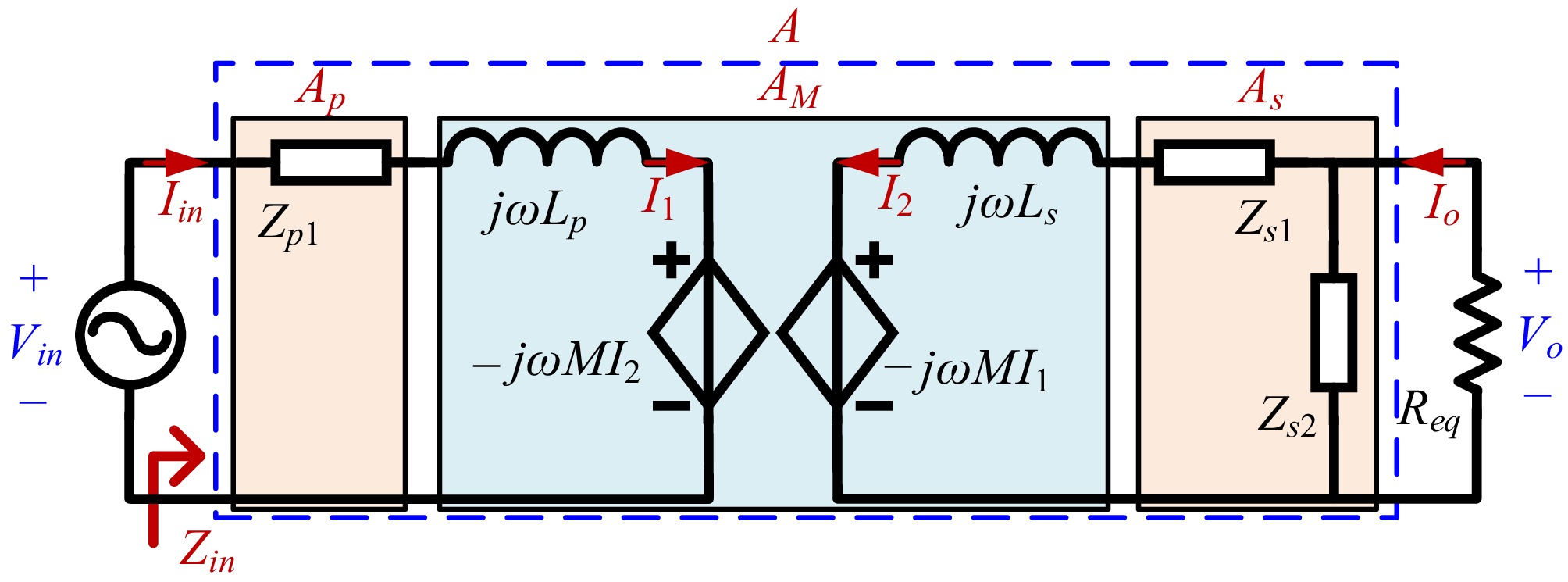
Figure 4.
Equivalent S/SP resonance circuit.
The transformation relationship of the two-port network illustrated in Fig. 4 can be formulated as a matrix representation:
$ \left[ \begin{gathered} {V_{in}} \\ {I_{in}} \\ \end{gathered} \right] = A\left[ \begin{gathered} {V_o} \\ {I_o} \\ \end{gathered} \right] $ (3) Where the transmission matrix A can be represented as
$ A = {A_p}{A_M}{A_s} = \left[ \begin{gathered} {a_{11}} \\ {a_{21}} \\ \end{gathered} \right.\left. \begin{gathered} {a_{12}} \\ {a_{22}} \\ \end{gathered} \right] $ (4) From the transformation relationships, the expressions for each of the matrix elements can be determined as:
$ \left\{ \begin{gathered} {a_{11}} = - {Z_m}\dfrac{1}{{{Z_{s2}}}} + Z'_{p1}\dfrac{{Z'_{s1} + {Z_{s2}}}}{{{Z_{s2}}}}\frac{1}{{{Z_m}}} \\ {a_{12}} = - {Z_m} + Z'_{p1}Z_{s1}^{'}\dfrac{1}{{{Z_m}}} \\ {a_{21}} = \dfrac{{Z'_{s1} + {Z_{s2}}}}{{{Z_{s2}}}}\dfrac{1}{{{Z_m}}} \\ {a_{22}} = Z'_{s1}\dfrac{1}{{{Z_m}}} \\ \end{gathered} \right. $ (5) The expressions for the respective intermediate variables are given by
$ \left\{ \begin{gathered} {Z_m} = j\omega M \\ Z'_{p1} = {Z_{p1}} + j\omega {L_p} \\ Z'_{s1} = {Z_{s1}} + j\omega {L_s} \\ \end{gathered} \right. $ (6) In order to obtain load-independent CC output and ZPA, the elements of the matrix need to meet the following conditions:
$ \left\{ \begin{gathered} {a_{11}} = 0 \\ {a_{22}} = 0 \\ \end{gathered} \right. $ (7) Combining Eqs (4)–(7), the impedance conditions for CC output and ZPA can be derived as
$ \left\{ \begin{gathered} Z'_{s1} = 0 \\ Z'_{p1}{Z_{s2}} = Z_m^2 \\ \end{gathered} \right. $ (8) Where, ZS2 is the reused reactance of the transformer magnetizing inductance, which is expressed as
$ {Z_{s2}} = j\omega {L_m} $ (9) According to Eq. (8), given the parameters of the coupled coils, the proposed S/SP compensated topology offers a higher degree of design freedom compared to the conventional S/S topology. CC output and ZPA can be achieved by satisfying the corresponding product relationship instead of a fixed parameter combination.
Upon satisfying the aforementioned design principle, the load-independent output current is given by
$ {I_o} = \dfrac{{{V_{in}}}}{{\left| {{a_{12}}} \right|}} = \dfrac{{{V_{in}}}}{{\omega M}} $ (10) Applying the proposed reuse design, the load-independent output current for the WPT system can be derived as
$ {I_L} = \dfrac{{8{V_{in}}}}{{{{\text π} ^2}\omega M}} $ (11) From the derived results, it is evident that load-independent CC output can be reliably achieved by meticulously designing the resonant compensation based on Eq. (8). This approach not only simplifies the output characteristics but also, when compared to conventional series-series compensation methods, significantly enhances the degree of design freedom offered by the proposed structure in this paper. This added flexibility allows for more versatile system optimization and adaptation to various operational requirements in wireless charging applications.
Based on the established parameter design principles, it can be understood that reactive power circulates within the coupling coils. This phenomenon results in a minor extra power loss when contrasted with the traditional S/S compensation topology. Nevertheless, given that the proposed system employs a full-wave rectifier with higher conversion efficiency, the overall DC-DC conversion efficiency of the complete system will not show a notable difference compared to a conventional S/S compensated WPT system.
ZPA operation
-
Drawing from the preceding derivations, it becomes evident that a multitude of parameter combinations are capable of achieving both CC output and ZPA. For the purpose of this analysis, one specific parameter combination has been selected and is meticulously presented in Table 1.
Table 1. A parameter combination following the proposed design methodology.
Part Value Part Value f 100 kHz Req 1.5–6.5 Ω Cp 25.3 nF Lp 120 μH Cs 21.1 nF Ls 120 μH M 20 μH Lc 20 μH With the reuse design above, the input impedance of the full-wave rectifier can be formulated as
$ {Z_{re}} = \dfrac{{j\omega M{R_{eq}}}}{{j\omega M + {R_{eq}}}} $ (12) The equivalent load Zin of the inverter can be expressed as
$ {Z_{in}} = ({Z_{re}} - j\omega M)||j\omega M $ (13) Zin can be simplified to:
$ {Z_{in}} = \dfrac{{\dfrac{{j\omega M{{\left( {\omega M} \right)}^2}}}{{j\omega M + {R_{eq}}}}}}{{\dfrac{{{{\left( {\omega M} \right)}^2}}}{{j\omega M + {R_{eq}}}} + j\omega M}} = \dfrac{{{{\left( {\omega M} \right)}^2}}}{{{R_{eq}}}} $ (14) Equation (14) indicates that the equivalent input impedance is resistive, which enables the system to realize ZPA at the designated frequency.
As illustrated in Fig. 5, the system's ability to maintain ZPA at the designated 100-kHz operating point is conclusively confirmed by the consistent input impedance angle observed across varying load conditions. This demonstrates the robust performance of the system in achieving resonant operation regardless of changes in the load. Besides maintaining ZPA consistently at 100-kHz, another zero-degree line exists. This implies that if the system operates at a frequency other than 100 kHz, the complex pulse frequency modulation is necessary to achieve load-independent ZPA. In such cases, CC output also cannot be guaranteed; thus, parameter design should not be based on this 0-degree line.
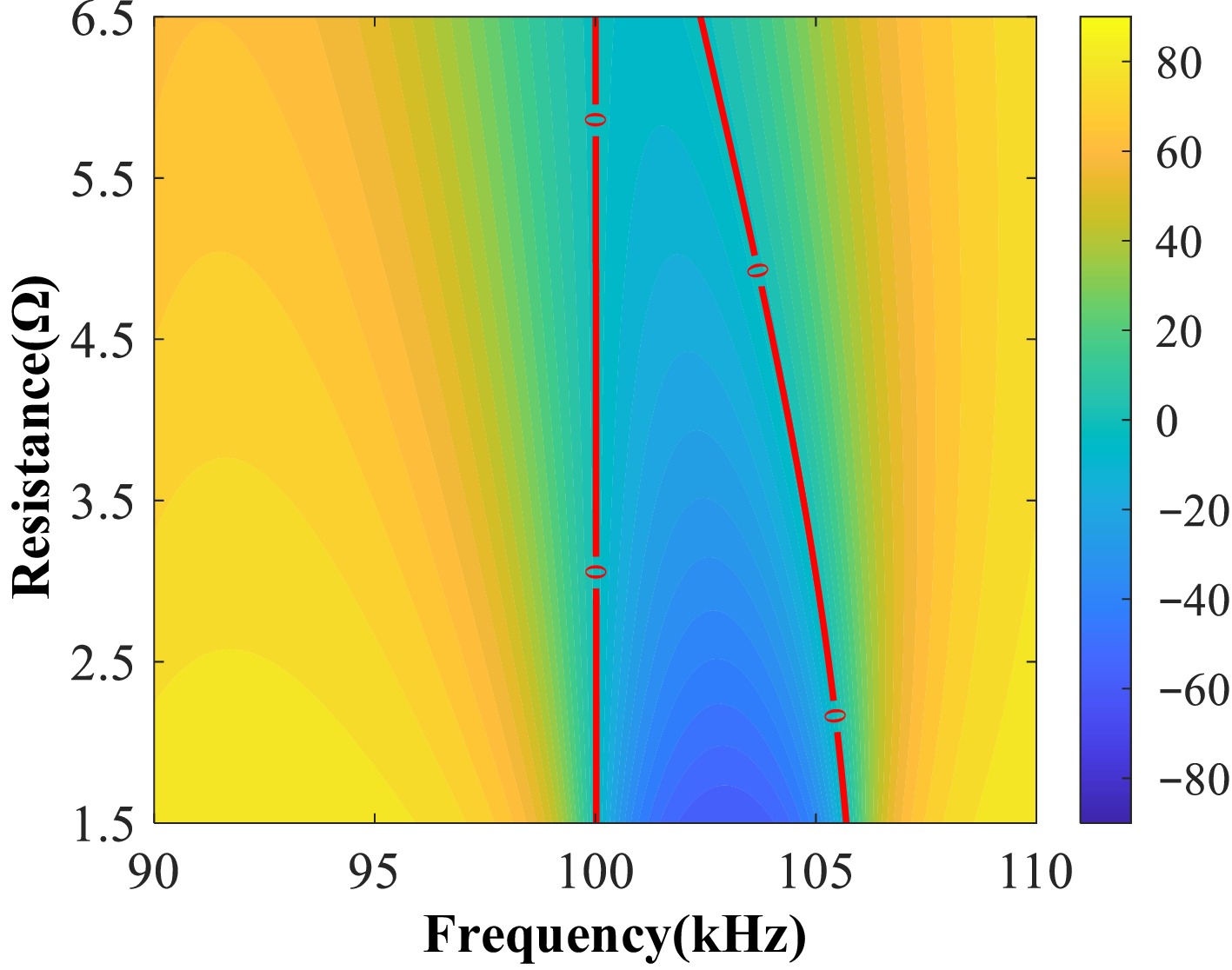
Figure 5.
Equivalent impedance angle (degrees) at varying loads and frequencies.
-
The experimental prototype, which faithfully reconstructs the WPT system illustrated in Fig. 2, is shown in Fig. 6. The center-tapped transformer for the full-wave rectifier in the prototype was designed based on the AP method, consistent with conventional full-wave rectifiers, yielding a turns ratio of 1:1:1.
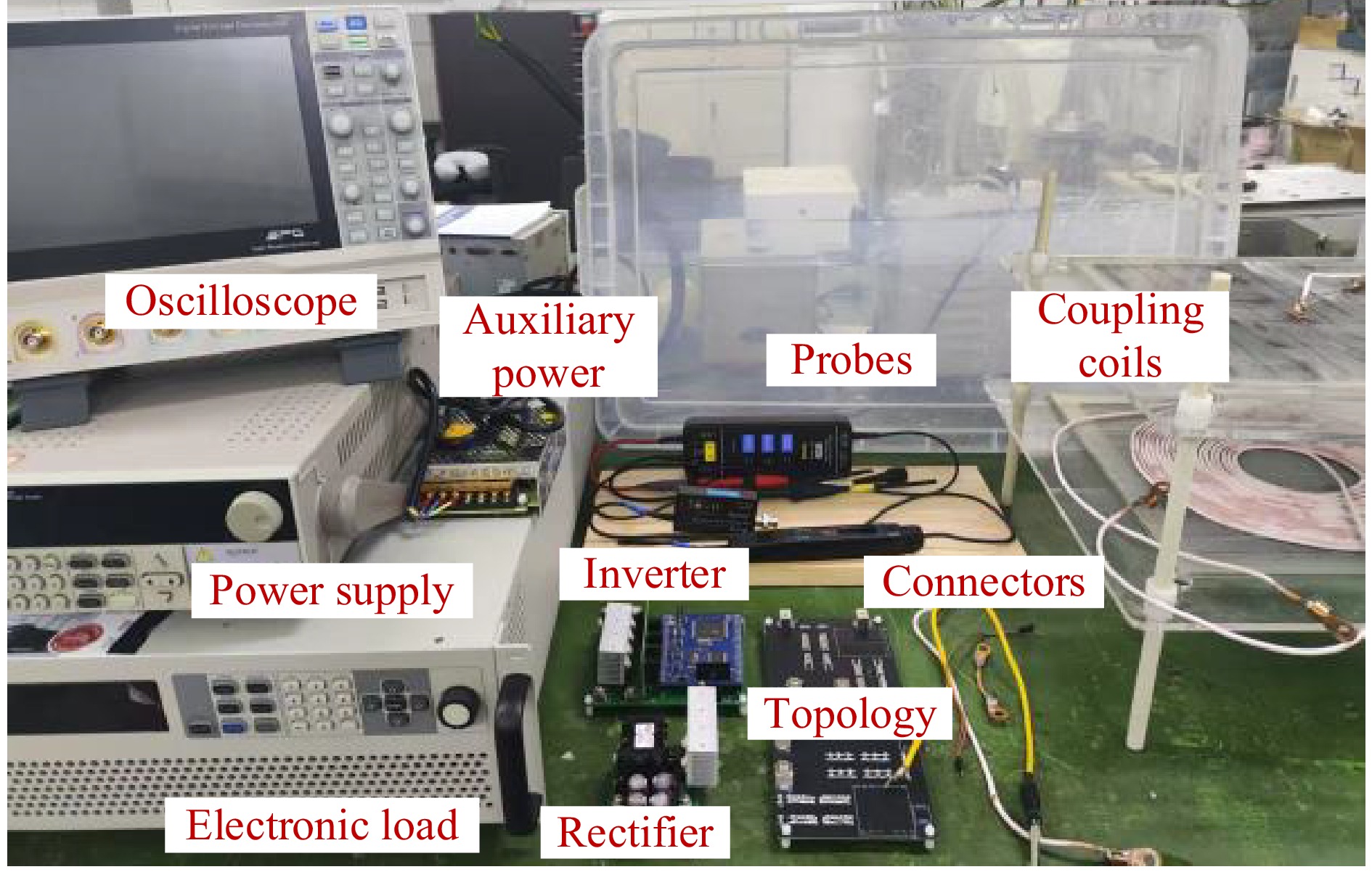
Figure 6.
Experimental prototype setup.
The full-wave rectifier utilizes a center-tapped transformer wound on a PQ35-35 ferrite core. The rectifier diodes are MBR20200CTG. The full-bridge inverter employs IRF640NPBF MOSFETs, driven by the IVCO1A02DR gate driver. Measurements were performed using an SDS2204X oscilloscope with a sampling rate set at 2 GSa/s. The relevant parameters listed in Table 2 are determined strictly according to the proposed design method.
Table 2. System parameters setup.
Part Value Part Value Vin 100 V ω 200π rad/s Cp 25.5 nF Lp 120.8 μH Cs 21.2 nF Ls 119.6 μH M 21.5 μH Lm 21.5 μH Cf 200 μF RL 2–8 Ω When the load resistances are 2-Ω, 5-Ω, and 8-Ω, respectively, the inverter output waveforms are shown in Fig. 7. The experimental results indicate that the inverter's equivalent load is weakly inductive, the system maintains a good resonant state, and no significant voltage spikes are observed at the inverter output.
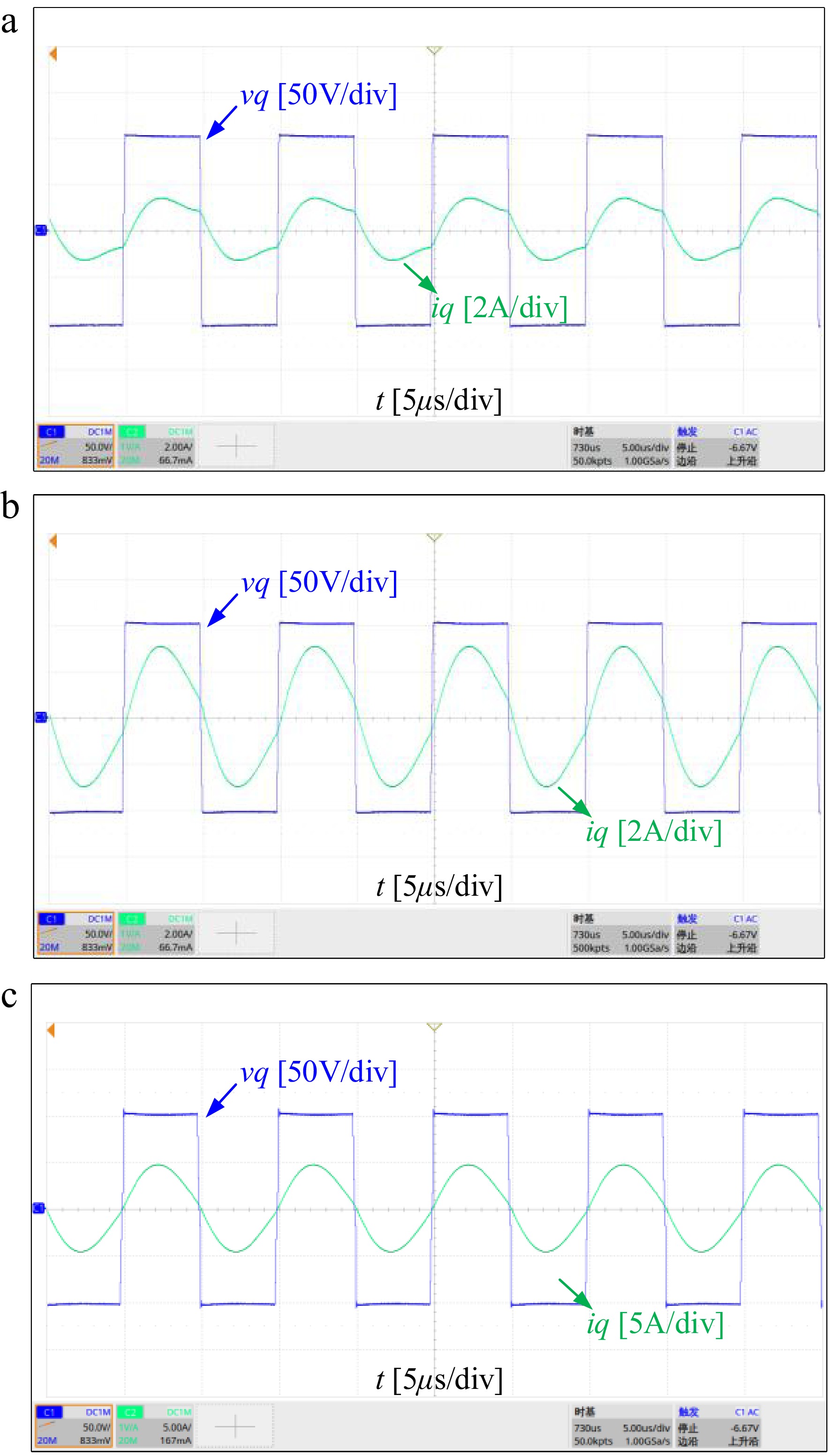
Figure 7.
The inverter output waveforms with different loads. (a) RL = 2-Ω. (b) RL = 5-Ω. (c) RL = 8-Ω.
Soft-switching operation of the inverter is typically characterized by the absence of voltage spikes in the output. As illustrated in Fig. 8, the VDS and VGS waveforms of the inverter's MOSFETs are measured under loads of 2-Ω, 5-Ω, and 8-Ω. The test results demonstrate that the inverter consistently achieves soft-switching operation throughout the specified load range. As the load increases, the prototype's soft-switching margin decreases. In practical applications, the soft-switching margin can be adjusted by tuning the relative values of the coupling coil mutual inductance M and the secondary impedance Zs1, thereby enabling high-efficiency inverter operation.
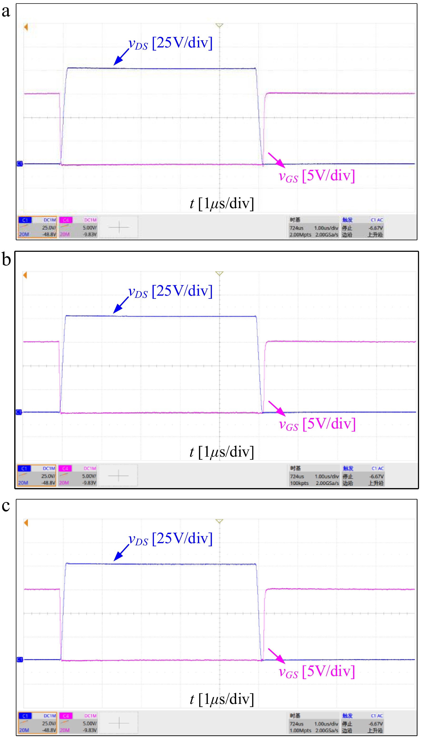
Figure 8.
VDS and VGS of inverter MOSFETs with different loads. (a) RL = 2-Ω. (b) RL = 5-Ω. (c) RL = 8-Ω.
The successful suppression of voltage spikes, coupled with the soft-switching operation of the inverter, serves as compelling validation for two key achievements: the realization of ZPA and the overall effectiveness of the proposed design method. This dual outcome underscores the robustness and precision of our approach.
A thorough evaluation confirms that the proposed WPT system achieves outstanding CC output performance. Across a significant load variation, spanning from 2-Ω to 8-Ω, the observed deviation of the output current from the desired 6A rated value is exceptionally small, consistently less than 0.1-A.
Moreover, the system's ability to maintain a stable transient output current when subjected to sudden load changes is a crucial attribute. This dynamic stability is visually and quantitatively demonstrated by the output waveforms depicted in Fig. 9, which illustrate its precise response to step-wise changes in load resistance.
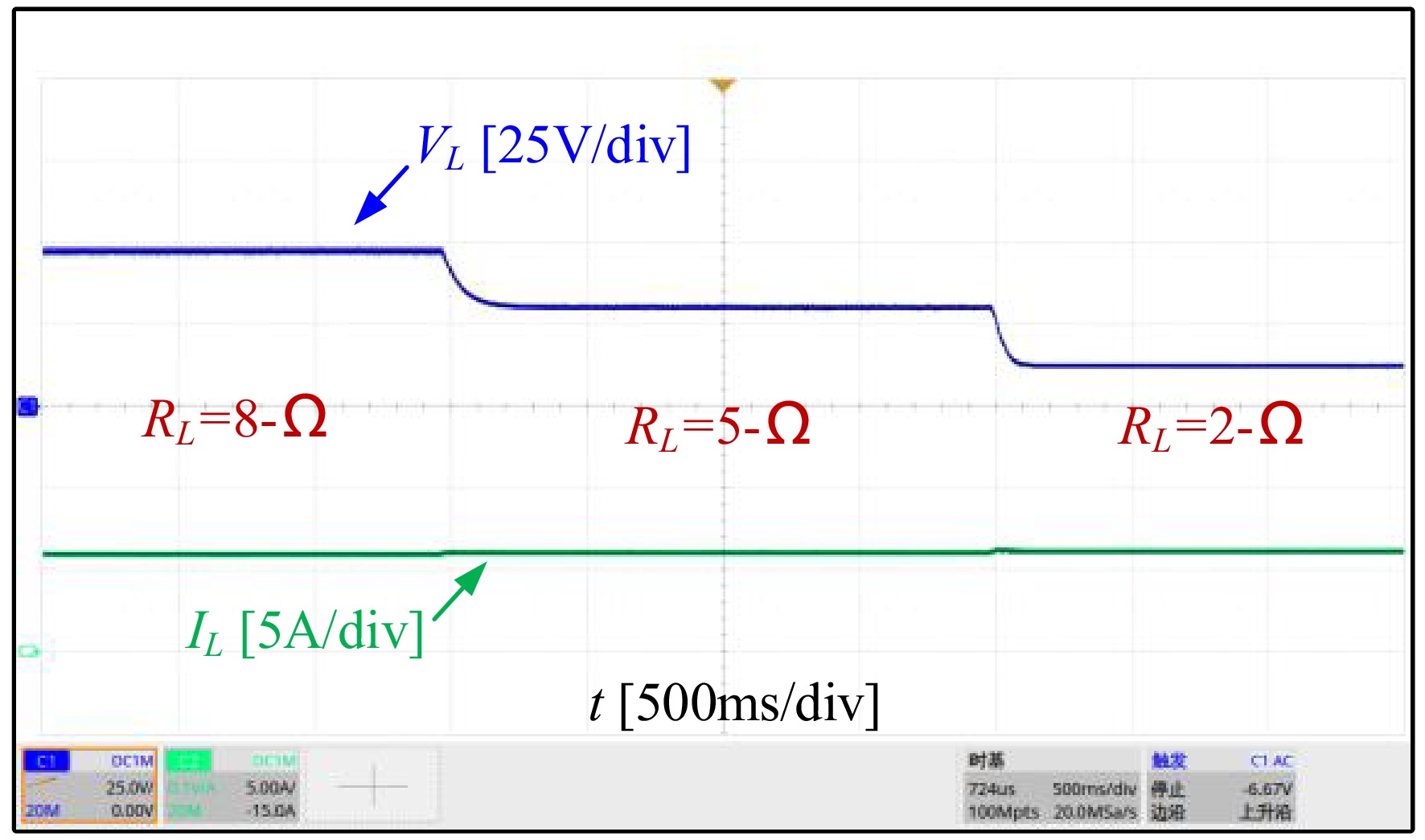
Figure 9.
Transient behaviors with step load.
A slight reduction in output current is observed with an increasing load. This phenomenon occurs because the input impedance of the rectifier can be characterized by an equivalent parallel resistance-inductance model. Consequently, as the load increases, the current diversion through the parallel inductive branch intensifies, leading to a marginal decline in output current.
Upon a sudden increase in load, a positive voltage spike is theoretically anticipated, attributed to the instantaneous surge in the charging current of the output filter. Nevertheless, given the ample design margin of the prototype's filtering components, no significant voltage spikes were observed during load step changes. The transient response also remained notably gradual.
In addition to the minimal output current fluctuation, the prototype exhibits high overall efficiency within the specified load range, as shown in Fig. 10a. Within this range, the system's output power increases rapidly with increasing load. However, due to the CC output, the rise in system losses is not particularly significant, resulting in a continuous upward trend in efficiency. At the rated 5-Ω load, as presented in Fig. 10b, the system achieves a conversion efficiency of up to 92.6%.
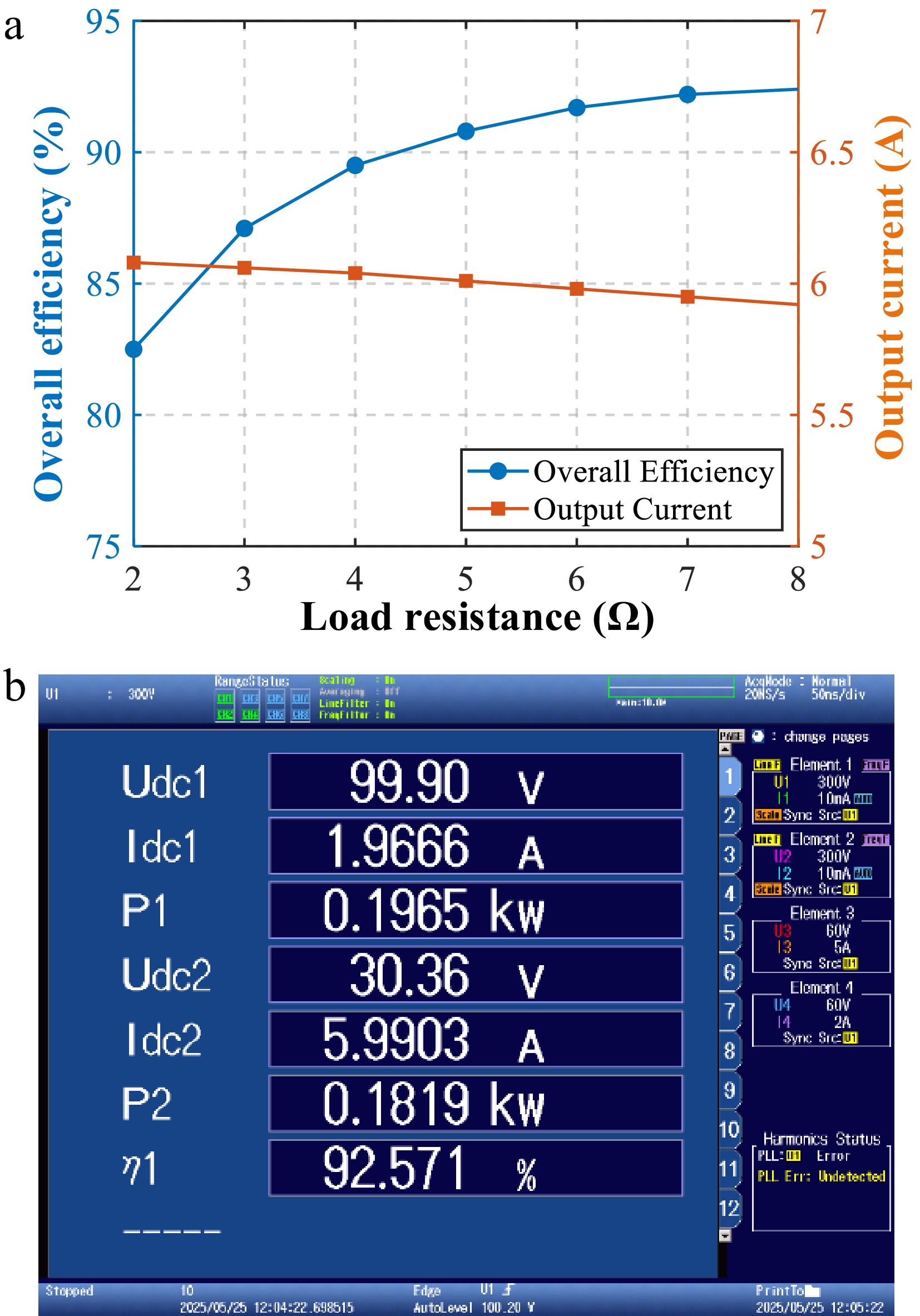
Figure 10.
System efficiency performance. (a) Overall efficiency with different loads. (b) The overall efficiency at rated load.
-
A novel design method is presented in this paper, wherein the magnetizing inductance of a full-wave rectifier structure transformer is repurposed as the resonant inductance for S/SP compensation. Both theoretical analysis and experimental validation confirm the significant efficacy of this approach. Distinct from conventional LCC/LCC and S/S compensation topologies, the S/SP configuration uniquely combines several benefits: CC output, inherent safety under open-circuit load conditions, and high efficiency. The integration with a full-wave rectifier and the ingenious reuse of the magnetizing inductance not only capitalize on the full-wave rectification's low power losses but also enable ZPA operation and inverter soft switching. It is anticipated that the proposed S/S compensation scheme, with the innovative reuse of the full-wave rectifier's magnetizing inductance, will offer a promising new avenue for the practical implementation of WPT systems.
-
A novel S/S compensation CC output scheme, which intelligently reuses the magnetizing inductance of a full-wave rectifier transformer, is presented in this paper. This design precisely integrates the full-wave rectifier transformer magnetizing inductance into the resonant network, while also compensating for the partial self-inductances of coupling coils, thereby enabling highly accurate CC output across a defined load spectrum. Experimental validation confirms the exceptional output stability and conversion efficiency of the proposed methodology. Specifically, a steady 6-A output current is maintained, with less than 1.3% fluctuation, throughout a load range of 2-Ω to 8-Ω. Furthermore, the inverter consistently maintains soft switching operation across this entire load range, contributing to high conversion efficiency, exemplified by a 92.6% efficiency at the rated 5-Ω load. This innovative reuse design holds significant promise as a practical solution for various applications.
The National Natural Science Foundation of China (Grant No. 52407198), China National Postdoctoral Program for Innovative Talents (Grant No. BX20230479), China Postdoctoral Science Foundation (Grant No. 2023M730848), Heilongjiang Postdoctoral Fund (Grant No. LBH-Z23163), Funding Project for 'Outstanding Master's and Doctoral Dissertations in the New Era of Longjiang' (Grant No. LJYXL2023-028). Supported by Self-Planned Task (Grant No. SKLRS202503B) of State Key Laboratory of Robotics and Systems (HIT).
-
The authors confirm their contributions to the paper as follows: study conception and design: Cai L; data collection: Mai J, Cui J; data analysis and interpretation: Cai L; draft preparation: Cai L, Cui J; manuscript review and editing: Guo C, Xu D. All authors reviewed the results and approved the final version of the manuscript.
-
The datasets generated during and/or analyzed during the current study are available from the corresponding author on reasonable request.
-
The authors declare that they have no conflict of interest.
- Copyright: © 2025 by the author(s). Published by Maximum Academic Press, Fayetteville, GA. This article is an open access article distributed under Creative Commons Attribution License (CC BY 4.0), visit https://creativecommons.org/licenses/by/4.0/.
-
About this article
Cite this article
Cai L, Mai J, Cui J, Guo C, Xu D. 2025. A constant-current WPT system with S/S compensated topology and full-wave rectification. Wireless Power Transfer 12: e034 doi: 10.48130/wpt-0025-0024 

A constant-current WPT system with S/S compensated topology and full-wave rectification
- Received: 03 June 2025
- Revised: 19 June 2025
- Accepted: 07 July 2025
- Published online: 31 December 2025
Abstract: In wireless charging applications, the constant current (CC) charging process is a critical stage that garners significant attention. This paper presents a novel S/SP compensation topology that achieves load-independent CC output, as well as offering significant design flexibility. To minimize rectification losses across the rectifier diodes during CC output, a full-wave rectifier structure is selected for the wireless power receiver. Building upon these considerations, this paper innovatively proposes an inductor reuse scheme between the S/SP compensation topology and the full-wave rectification structure. The proposed reuse design approach enables zero phase angle (ZPA) operation and configures the wireless power transfer (WPT) system as a cascaded arrangement of an S/S compensation topology and a full-wave rectifier. The efficacy of the proposed design is validated using a 6-A CC output prototype, and experimental results demonstrate a maximum ±1.3% output current fluctuation. The prototype achieves inverter soft-switching operation and a 94.2% peak efficiency across a four-fold load variation range.