-
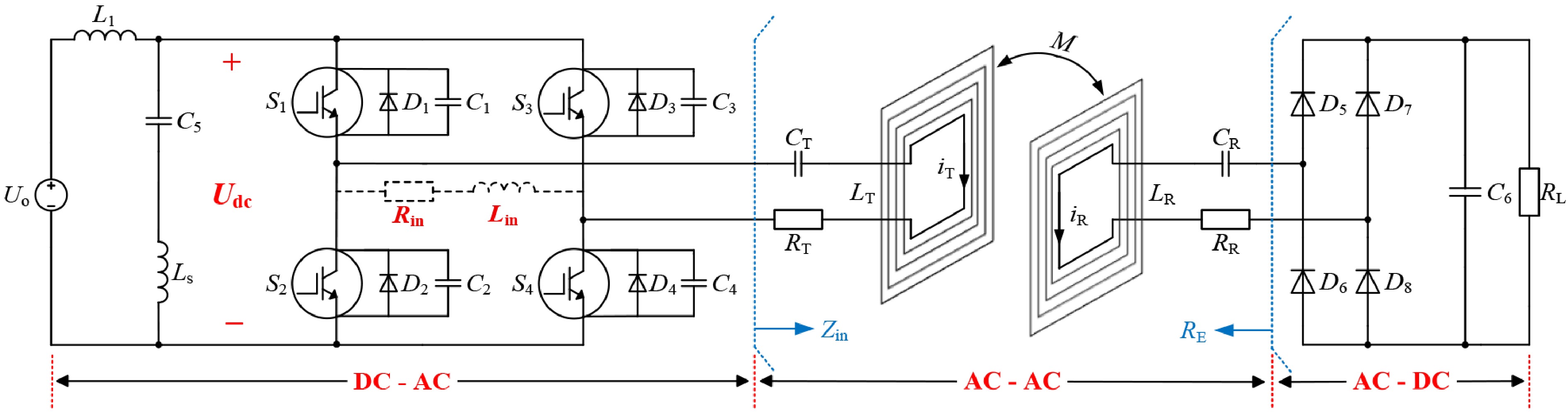
Figure 1.
A typical S-S type WPT system circuit topology diagram used for analysis in this paper.
-
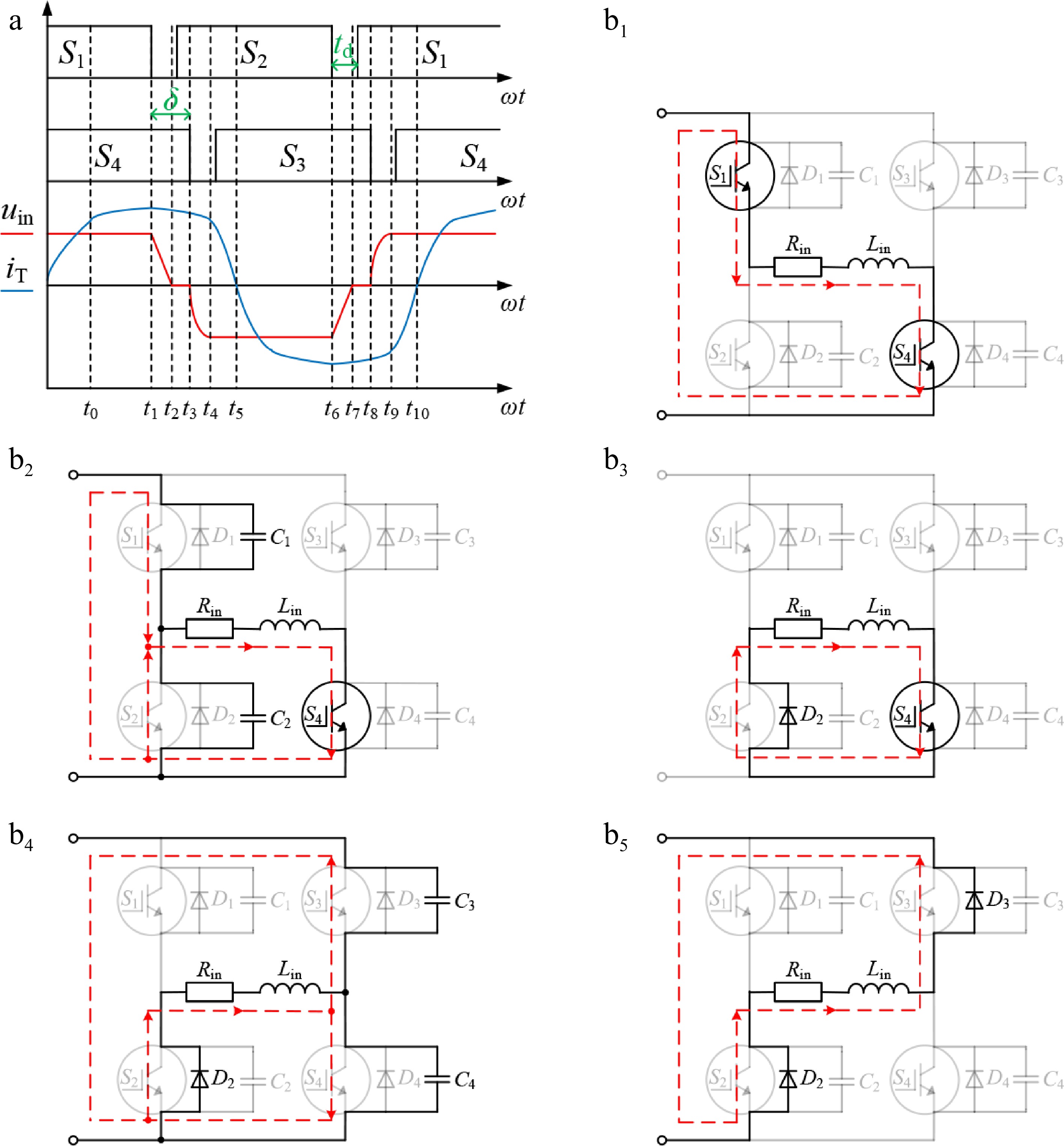
Figure 2.
Main current paths in the inverter circuit. (a) Inverter steady-state output waveform diagram. (b) Current paths in different operating modes within half a cycle. (b1) Mode 1, corresponding to t0−t1. (b2) Mode 2, corresponding to t1−t2. (b3) Mode 3, corresponding to t2−t3. (b4) Mode 4, corresponding to t3−t4. (b5) Mode 5, corresponding to t4−t5.
-
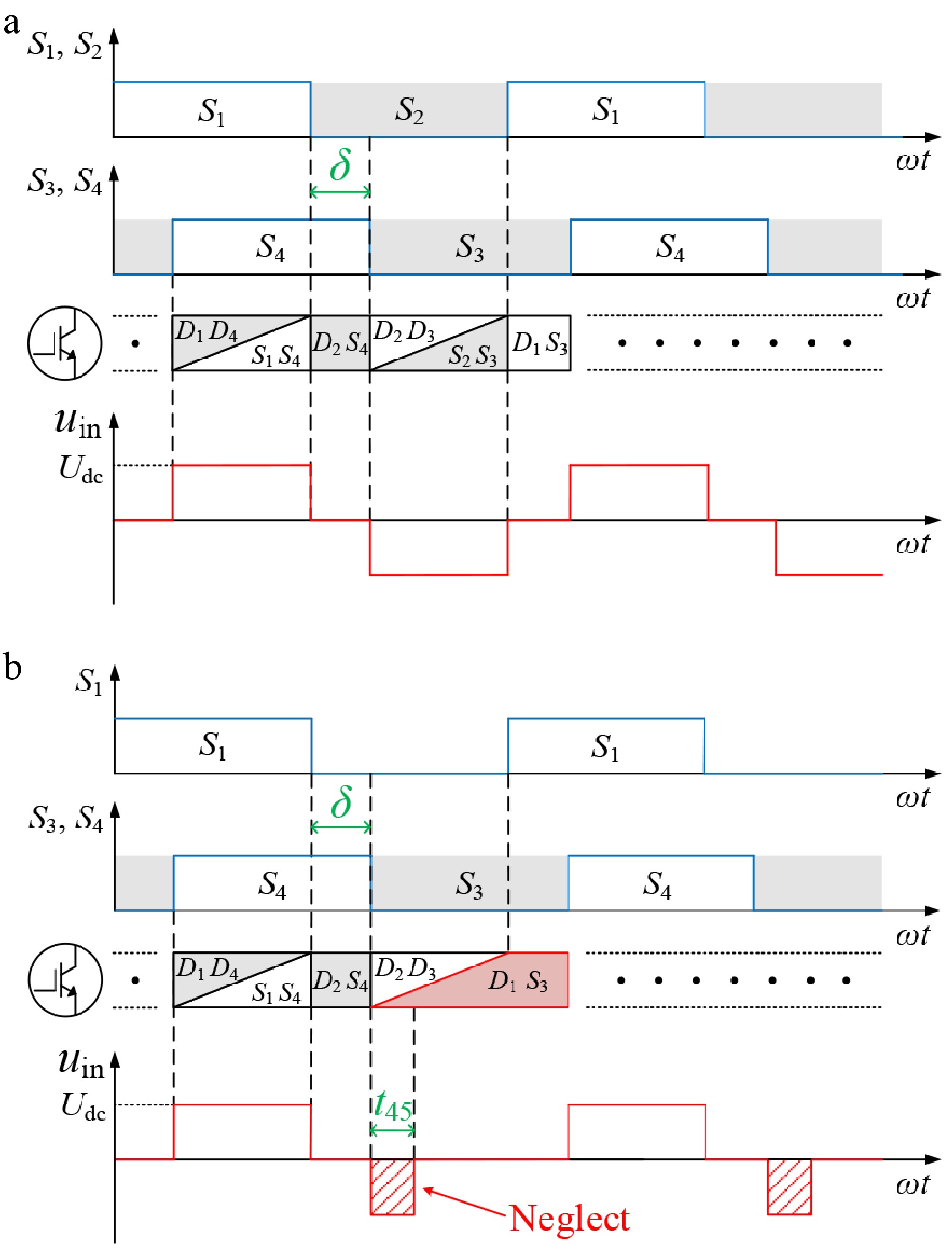
Figure 3.
PWM waveforms of switching devices under different operating conditions. (a) Normal working conditions. (b) S2 OC fault condition.
-
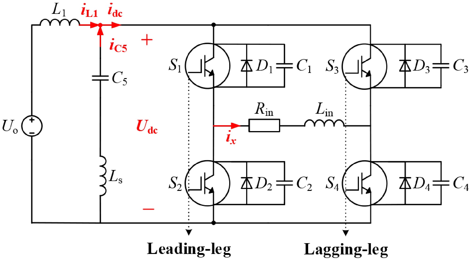
Figure 4.
Equivalent circuit topology of the WPT system used to establish the diagnostic model.
-
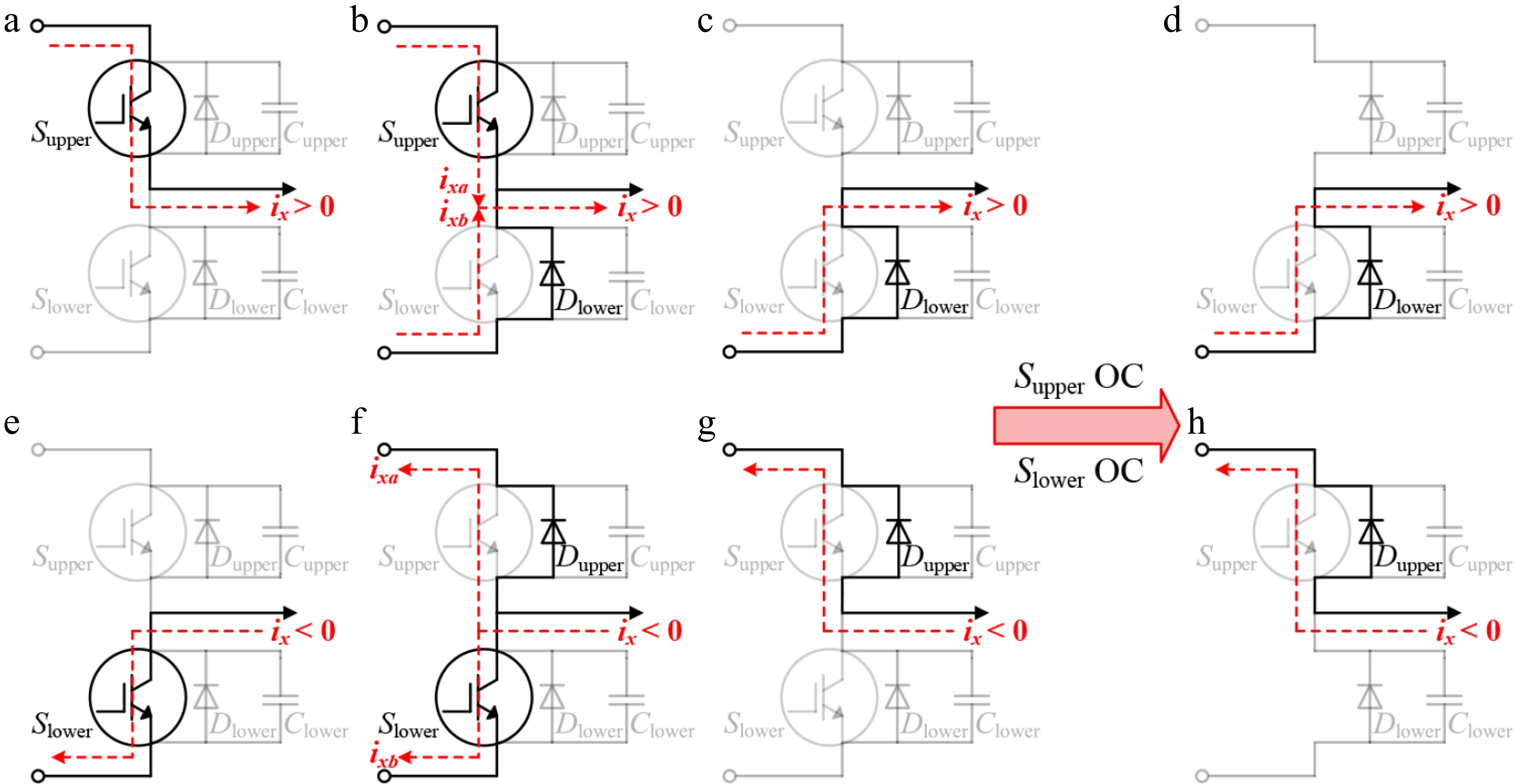
Figure 5.
Main current paths of the WPT system diagnostic model under different operating conditions. ix > 0: (a) Sx = 1; (b) Sx = 1 to 0; (c) Sx = 0; (d) Supper OC. ix < 0: (e) Sx = 0; (f) Sx = 0 to 1; (g) Sx = 1; (h) Slower OC.
-
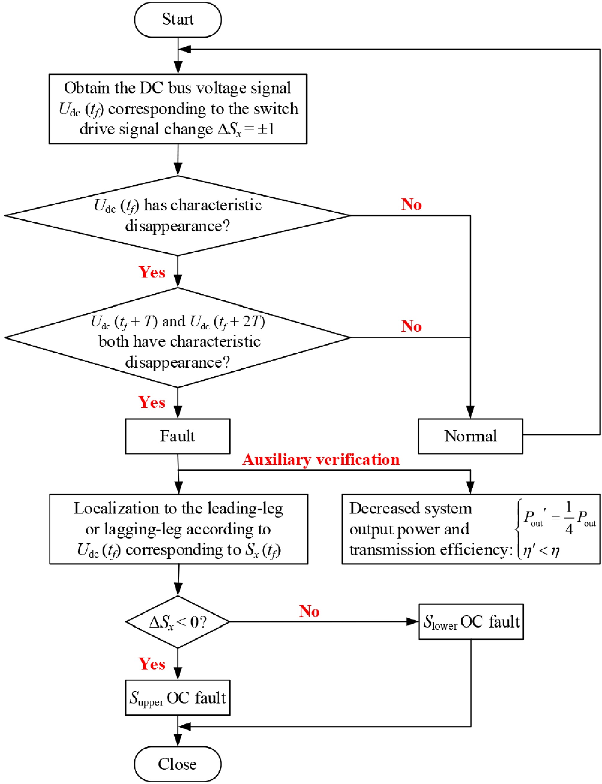
Figure 6.
Flowchart of WPT system fault diagnosis and localization strategy.
-
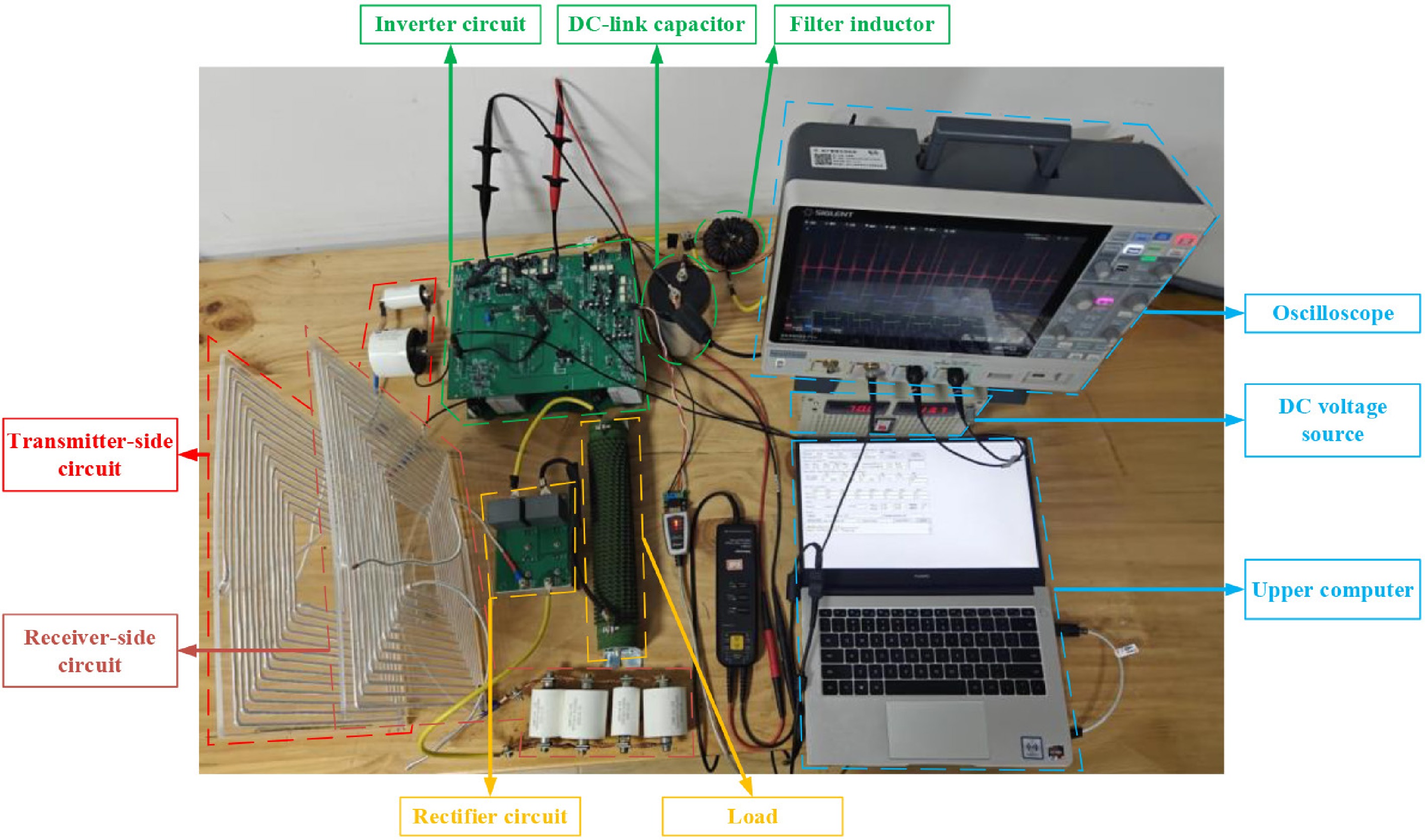
Figure 7.
Experimental platform for method validation.
-
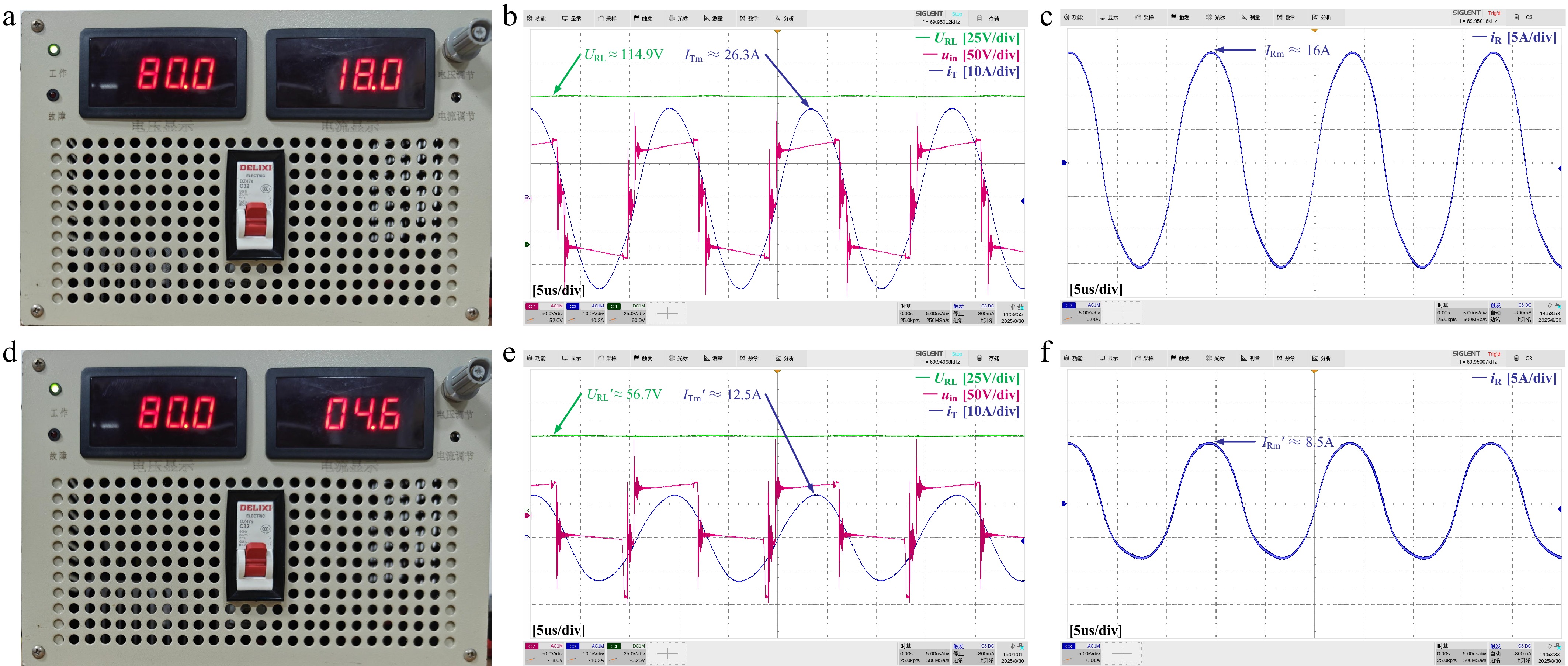
Figure 8.
Relevant electrical parameters for power and efficiency calculations. (a)–(c) Normal operating case. (d)–(f) S2 OC case. (a) DC voltage source output voltage Uo and output current Io. (b) Load voltage URL, inverter circuit output voltage uin, and transmitter-side loop current iT. (c) receiver-side loop current iR. (d) DC voltage source output voltage Uo' and output current Io'. (e) Load voltage URL', inverter circuit output voltage uin', and transmitter-side loop current iT'. (f) receiver-side loop current iR'.
-
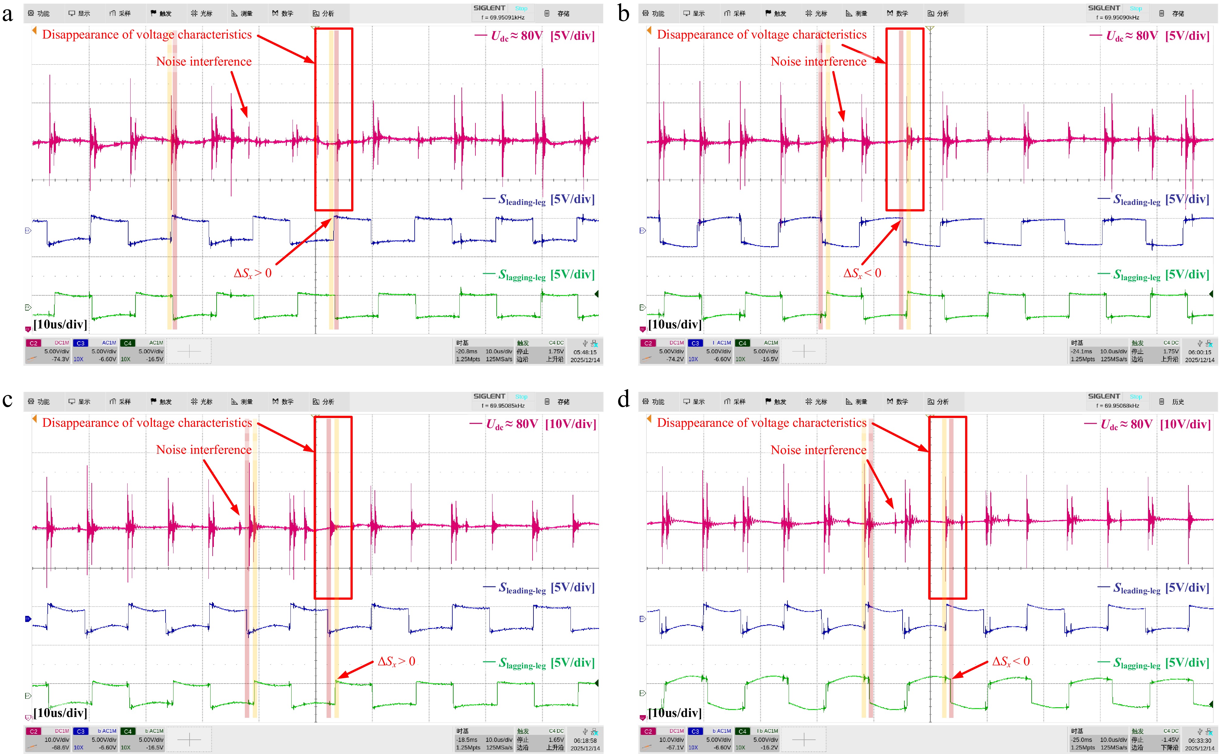
Figure 9.
Experimental results for OC fault in each switching transistor under different coupling coefficients. (a) k = 0.384, S2 OC case. (b) k = 0.235, S1 OC case. (c) k = 0.158, S4 OC case. (d) k = 0.098, S3 OC case.
-
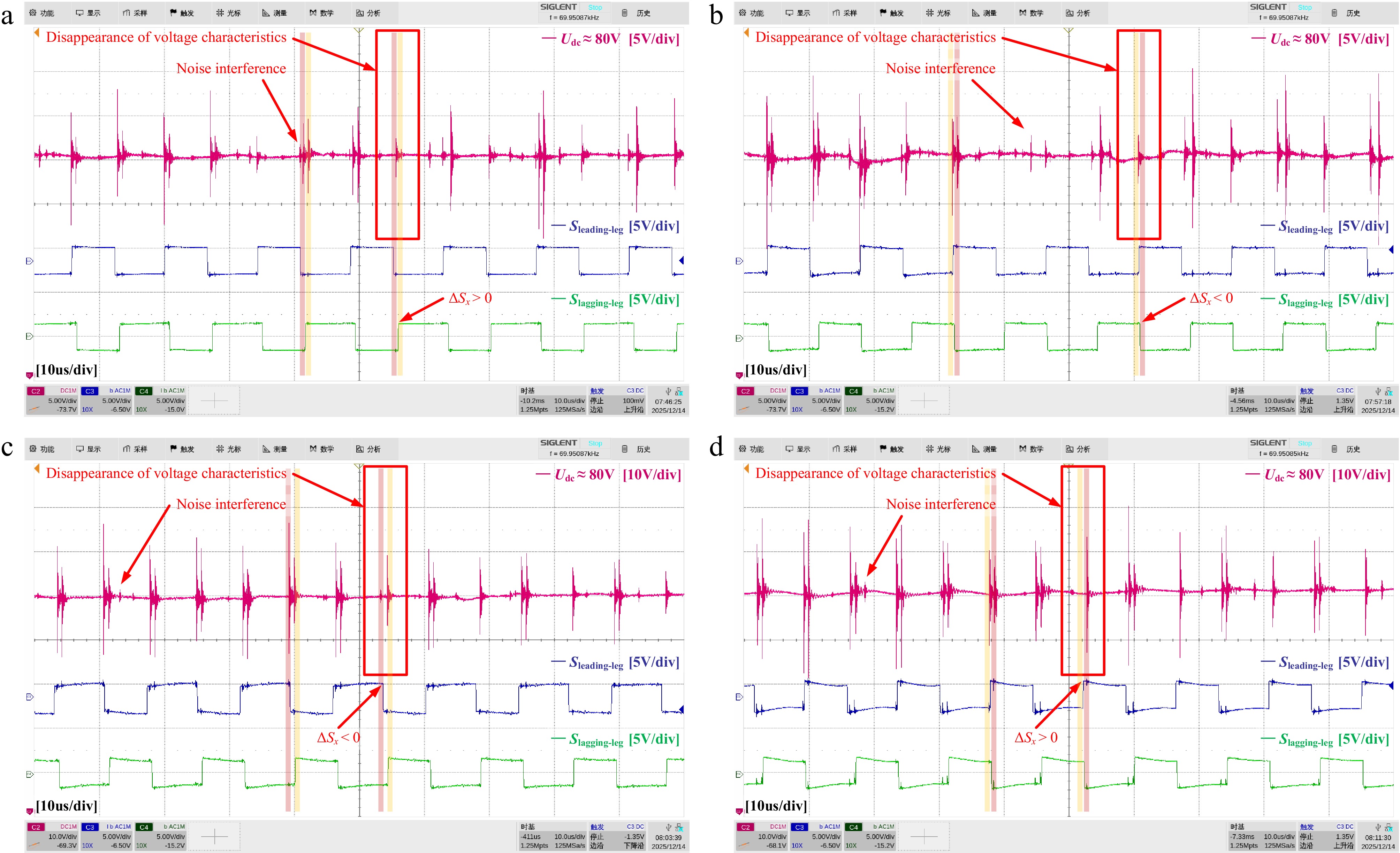
Figure 10.
Experimental results for OC fault in each switching transistor under different load resistances. (a) RL = 5.5Ω, S4 OC case. (b) RL = 10.4Ω, S3 OC case. (c) RL = 15.7Ω, S1 OC case. (d) RL = 20.1Ω, S2 OC case.
-
Parameters Value Parameters Value Uo (V) 80 f (kHz) 70 δ (°) 19 td (ns) 551 L1 (mH) 0.3 rL1 (Ω) 0.002 C5 (mF) 0.5 rC5 (Ω) 0.013 LS (nH) 218 rIGBT (Ω) 0.06 tr (ns) 9 tf (ns) 15 Cce (pF) 445 M (μH) 4.2~16.5 RT (Ω) 0.06 RR (Ω) 0.07 LT (μH) 42.7 LR (μH) 43.2 CT (nF) 128.8 CR (nF) 120.1 UD (V) 1.7 rD (Ω) 0.005 C6 (μF) 50.2 rC6 (Ω) 0.005 RL (Ω) 5.5~20.1 k 0.098~0.384 Table 1.
Experimental platform parameters.
-
Ref. Feature parameters Diagnosis time Software and hardware costs Logical judgment [18] DC bus voltage difference residual Three switching cycles Medium Comlex [19] DC capacitor voltage One current cycle Medium Moderate [20] DC bus voltage, output current Half to two current cycles Small Moderate [21] DC bus voltage, three-phase current One switching cycle Large Moderate Proposed DC bus voltage Three switching cycles Small Simple Table 2.
Performance comparison of similar methods.
Figures
(10)
Tables
(2)