-
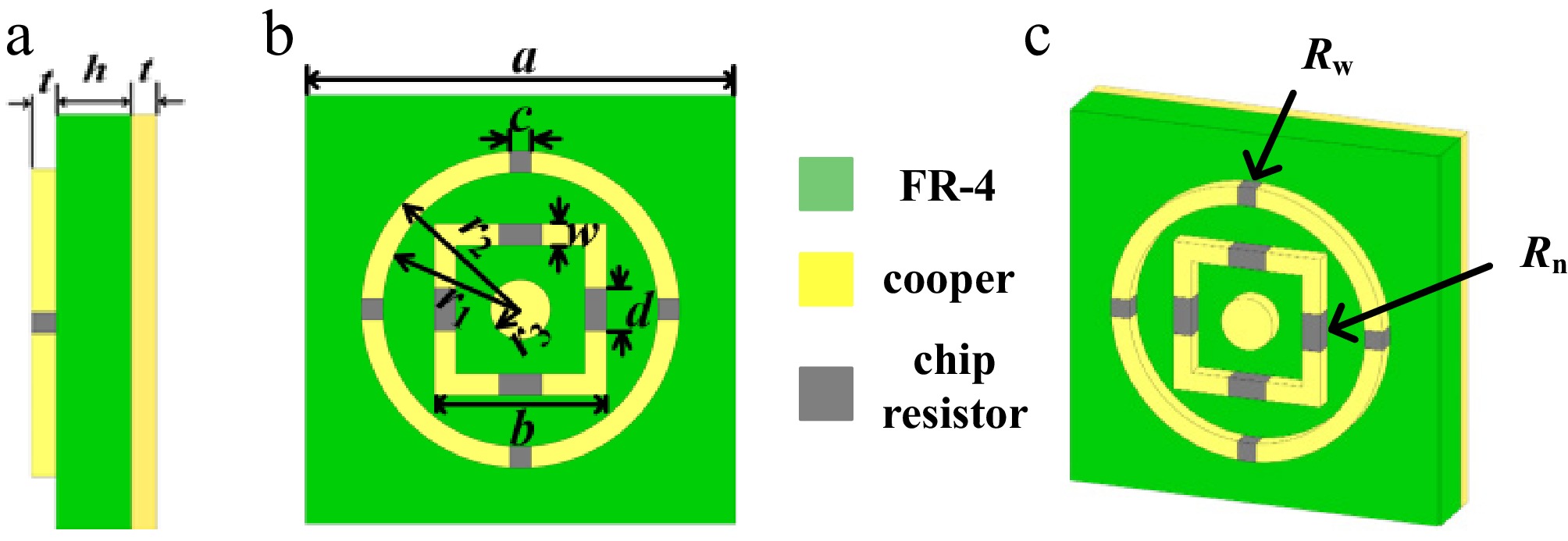
Figure 1.
Schematic diagram of the designed resonant unit. (a) Top view. (b) Side view. (c) Overall structure view.
-
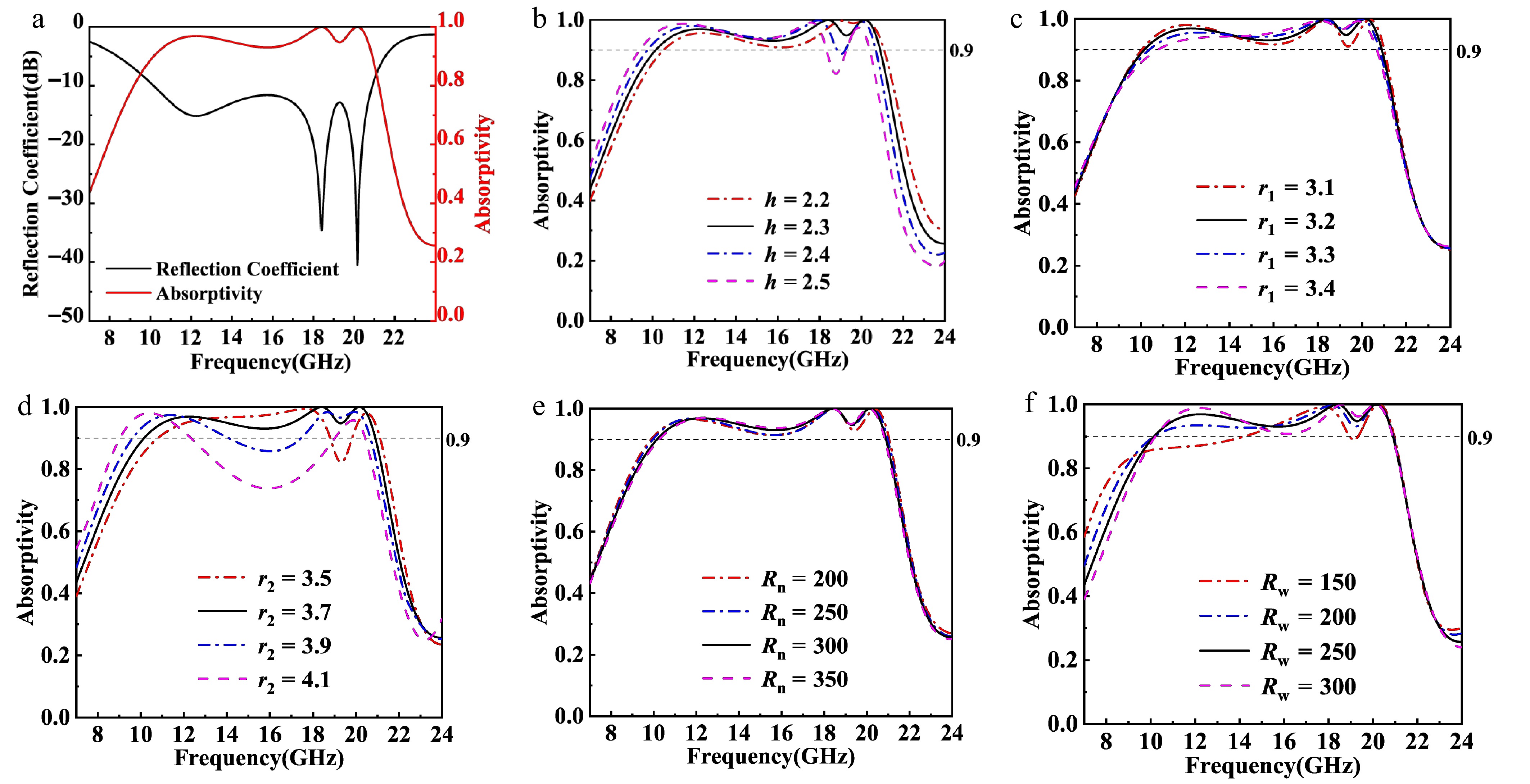
Figure 2.
Reflection coefficient and absorptivity of the absorber at different parameters. (a) Optimized structural parameters, (b) h, (c) r1, (d) r2, (e) Rn, and (f) Rw.
-
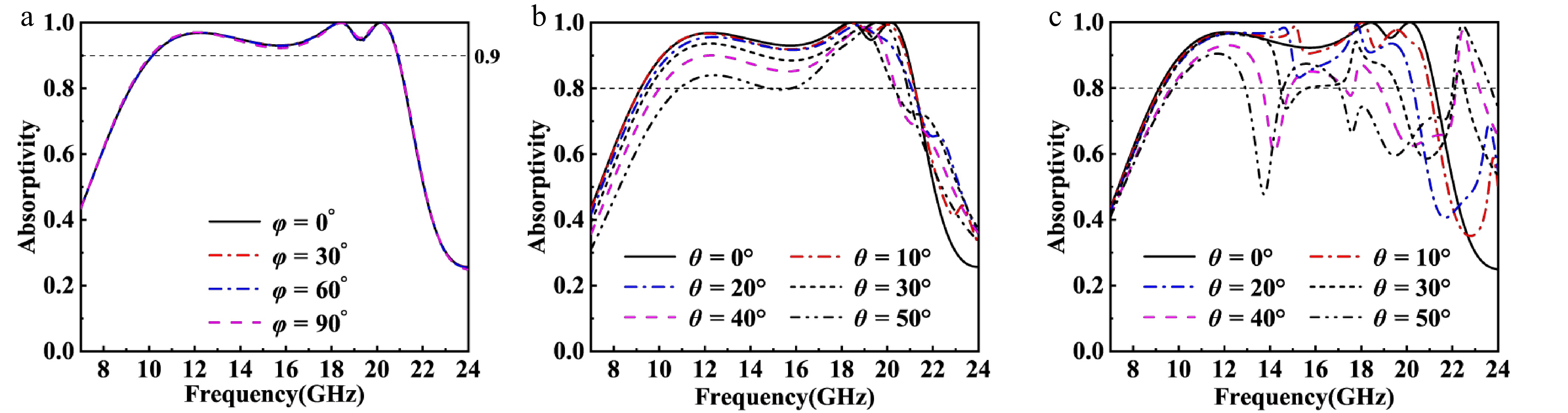
Figure 3.
Absorptivity of the absorber at different (a) polarization angles, (b) incidence angles in TE mode, and (c) incidence angles in TM mode.
-
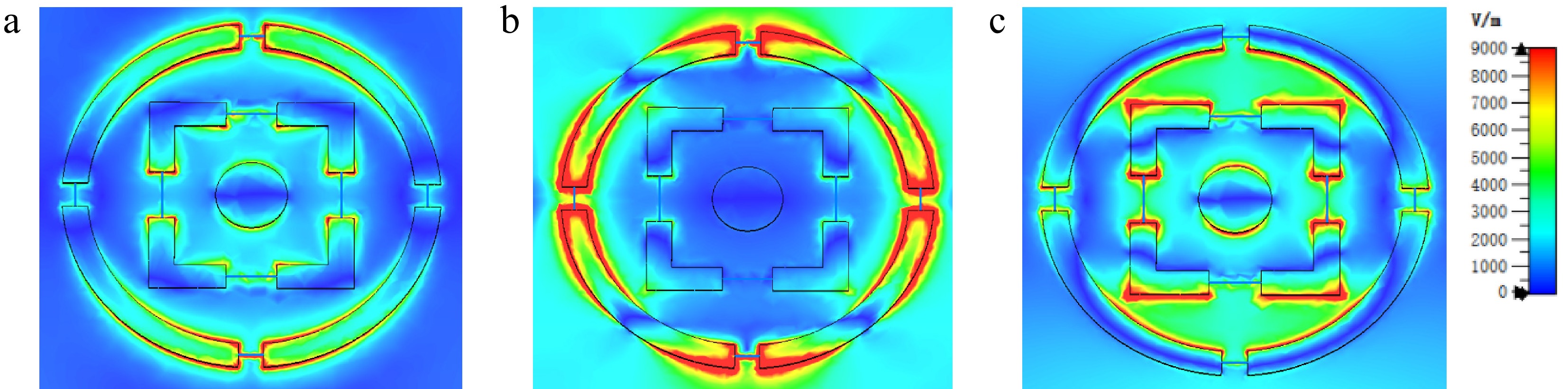
Figure 4.
Electric field distribution at three resonance frequencies. (a) 12.24 GHz, (b) 18.4 GHz, and (c) 20.16 GHz.
-
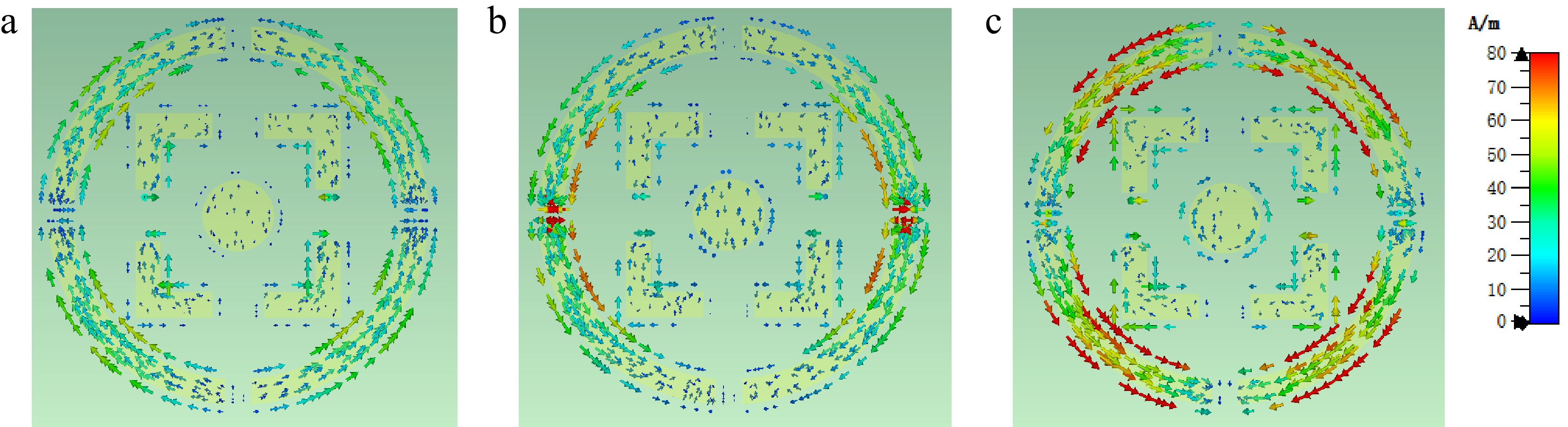
Figure 5.
The surface current density distribution (a) 12.24 GHz, (b) 18.4GHz, and (c) 20.16 GHz.
-
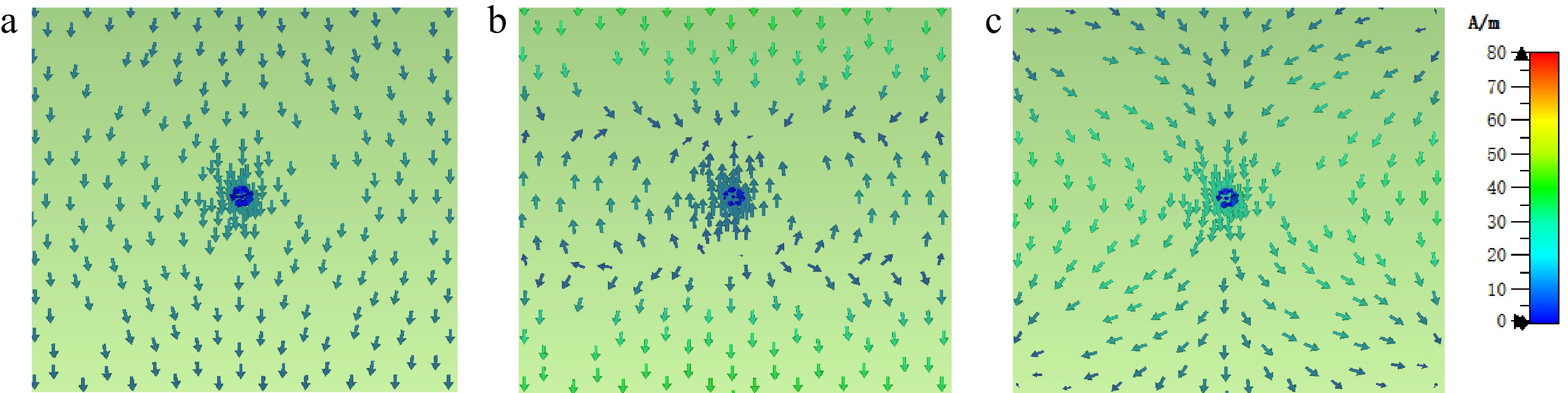
Figure 6.
The backplane current density distribution (a) 12.24 GHz, (b) 18.4 GHz, and (c) 20.16 GHz.
-
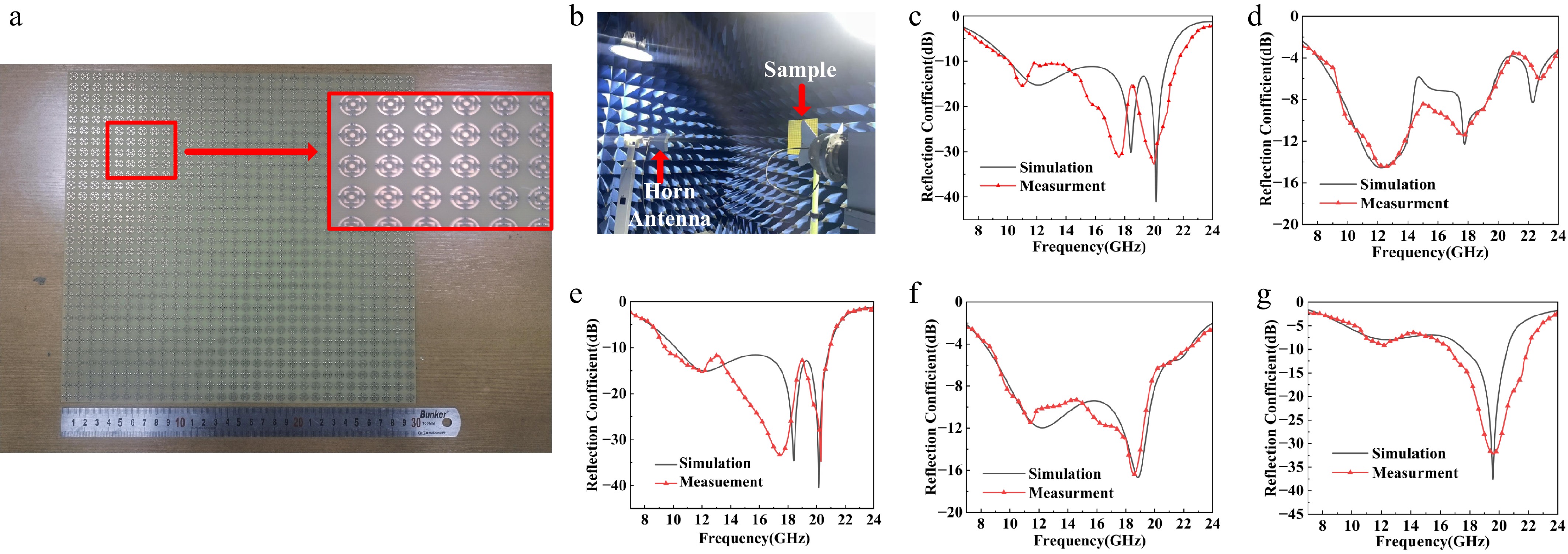
Figure 7.
Experimental tests and results; (a) absorber sample, (b) experimental setup, (c) 0° angle of incidence in TM mode, (d) 30° angle of incidence in TM mode, (e) 0° angle of incidence in TE mode, (f) 30° angle of incidence in TE mode, and (g) 50° angle of incidence in TE mode.
-
Ref. Bandwidth (GHz) FBW (%) Oblique incidence Thickness (mm) Electrical thickness Structural materials Fabrication features TE TM [24] 11.4−20 54.8% 50° 50° 1.6 0.084λ0 FR-4 and metal Single layer [27] 4.3−11.1 88.3% 60° 60° 9.48 0.243λ0 PVC/ITO/OCA/PET Double-layer [28] 5.10−14.07 94% N/A N/A 6.6 0.211λ0 Rossler chaos surface Chaotic units [25] 12.35−14.65 17% 45° 45° 2 0.09λ0 FR-4 and metal Single layer [26] 8.9−14.0 44.5% 50° 60° 1.6 0.061λ0 ITO and substrate Single layer This work 10.15−20.91 69.3% 50° 30° 2.3 0.119λ0 FR-4 and metal Single layer Table 1.
Comparison of broadband absorbers.
Figures
(7)
Tables
(1)