











-
Electromagnetic radiation in communication systems can couple into equipment through closed-loop paths during operation, leading to electromagnetic compatibility issues[1]. Metasurface absorbers have emerged as an effective solution due to their compact size and high absorption rate. By tailoring artificial structures to modify their equivalent electromagnetic parameters, these absorbers exhibit distinct electromagnetic properties and have increasingly been applied in fields such as invisibility cloaks[2], metamaterial 'perfect' absorbers[3,4], wireless power transfer[5], satellite communication, and radar surveillance[6].
Although some absorbers are designed with flexible structures to accommodate bending applications, this flexibility often results in increased thickness and reduced absorption bandwidth[7], limiting their performance in complex and dynamic electromagnetic environments. Conversely, absorbers characterized by broad absorption bandwidths and compact geometries demonstrate superior environmental adaptability. During the design process, factors such as cost-effectiveness and manufacturability must also be carefully considered. Under natural resonance, metamaterial absorbers exhibit an inherently narrow absorption bandwidth. To overcome this issue, superior materials and multilayer stacking can be used to broaden the absorption bandwidth. By incorporating materials with favorable electromagnetic properties, such as ITO, PET, VO2, SiO2, and PMI[8−12], the electromagnetic parameters of the absorber can be improved, thereby broadening its absorption bandwidth. Nevertheless, in practical fabrication, materials such as PET and ITO, despite their excellent electromagnetic properties, often require more complex manufacturing processes. This not only significantly increases production costs but also introduces substantial challenges to the overall fabrication process. Therefore, while these materials enhance broadband absorption, their inclusion requires an economic trade-off. By stacking multilayer materials[13] or multilayer resonant topologies[14−19], each layer contributes to absorption in different frequency bands, enabling distinct electromagnetic wave absorption mechanisms and thereby enhancing the overall absorption performance. However, this approach increases the size and mass of the absorber, and the multilayer structure typically requires sophisticated manufacturing processes. The design of each layer has to take into account factors such as interlayer compatibility and material adaptation. Inadequate coupling between layers may weaken absorption in certain frequency bands, limiting bandwidth enhancement or even causing bandwidth contraction, ultimately degrading overall performance and absorption efficiency. Currently, the absorber topology design based on lumped elements offers an effective approach to broadening the absorption bandwidth; for example, symmetric semicircular structures with pin diodes[20] and open-ring or metal-strip configurations with chip resistors[21]. Despite these approaches' ability to expand the absorption bandwidth, they often lead to increased structural complexity and thickness[22]. Therefore, the design of an absorber based on lumped elements should be characterized by both broadband absorption, simplicity of structure, and small thickness.
In this work, a single-layer absorber based on lumped elements is proposed. The proposed absorber achieves over 90% absorption in the frequency range of 10.15–20.91 GHz, corresponding to a fractional bandwidth of 69.3%, with a total thickness of 2.3 mm and an electrical thickness of 0.119 λ0, where λ0 is the wavelength corresponding to the center frequency of the absorber's operating bandwidth. Experimental validation confirms its performance, demonstrating broadband operation, structural simplicity, wide-angle stability, and polarization insensitivity.
-
Figure 1 shows the top view, side view, and overall structural configuration of the proposed metasurface absorber unit. The unit consists of a metal resonant layer, a dielectric layer, a metal reflective layer, and chip resistors. The metal resonant unit includes an outer split ring, within which is nested a split square ring, a central metal disc, and eight chip resistors. The eight chip resistors are symmetrically placed at the split gaps of the two rings—four on the outer circular ring and four on the inner square ring—providing conductive bridging across the splits and contributing to the broadband absorption performance. They are loaded at eight splits from the outside to the inside. The resistors on the circular ring are denoted as Rw, and those on the square ring are denoted as Rn. Considering the fabrication cost as well as the fabrication process, FR-4 material with a relative dielectric constant of 4.3 and a loss tangent of 0.025 was selected for the dielectric layer. The metal resonance layer and the reflection layer are made of metallic copper. The size of the resonance unit is 10 mm × 10 mm. The values of the parameters identified in Fig. 1 are a = 10 mm, t = 0.035 mm, h = 2.3 mm, w = 0.5 mm, r1 = 3.2 mm, r2 = 3.7 mm, b = 4 mm, r3 = 0.7 mm, c = 0.5 mm, and d = 1 mm.
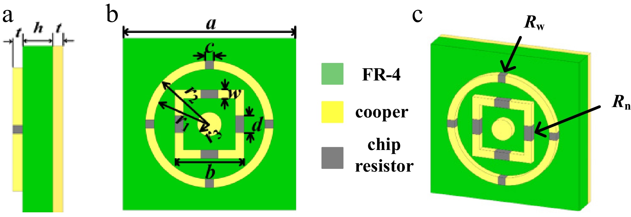
Figure 1.
Schematic diagram of the designed resonant unit. (a) Top view. (b) Side view. (c) Overall structure view.
To obtain the electromagnetic wave absorption performance, the designed broadband metasurface absorber is modeled using CST Studio Suite. Fig. 2 illustrates the absorption performance of the optimal parameters. The absorption rate is calculated by:
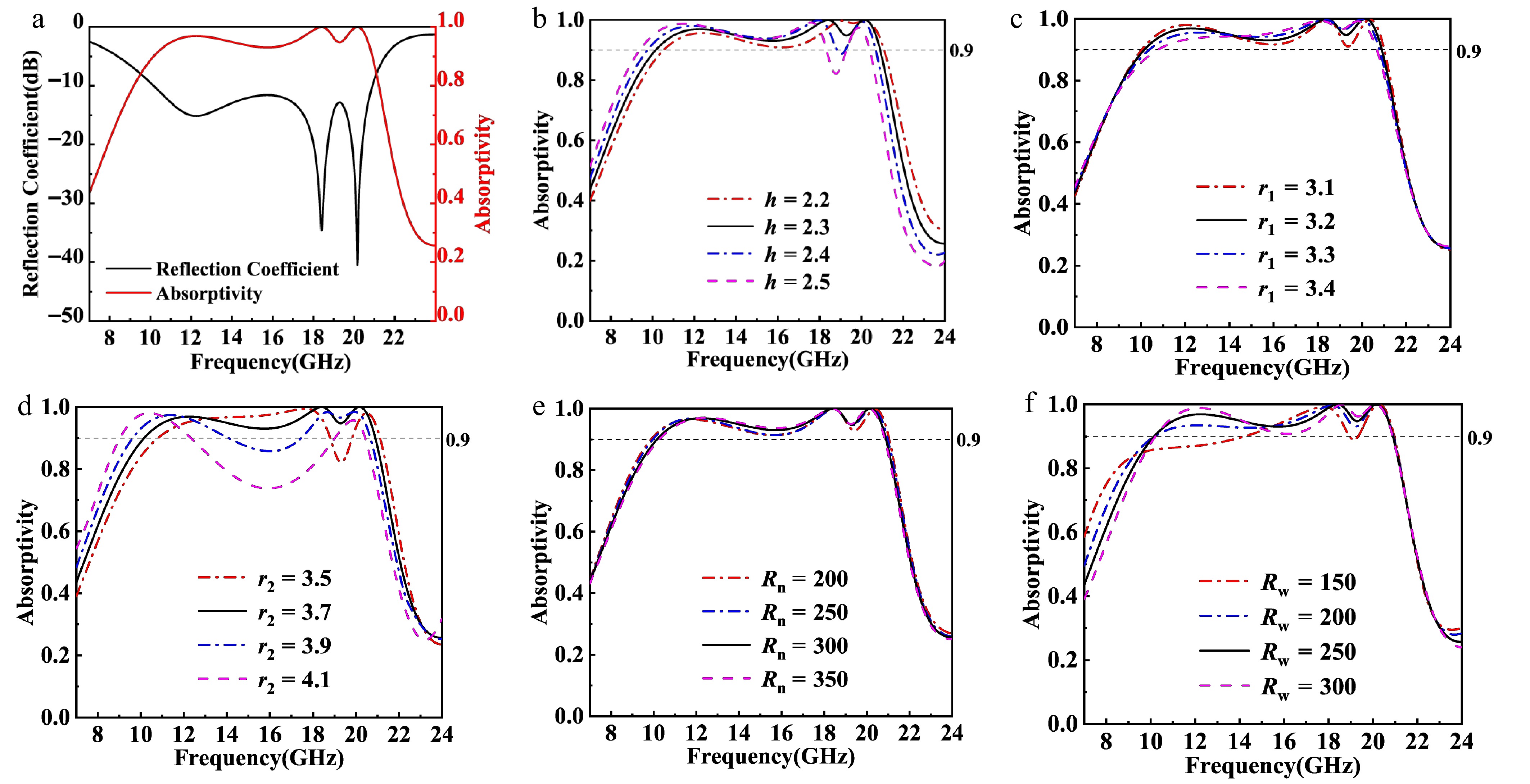
Figure 2.
Reflection coefficient and absorptivity of the absorber at different parameters. (a) Optimized structural parameters, (b) h, (c) r1, (d) r2, (e) Rn, and (f) Rw.
$ A(\omega )=1-\Gamma (\omega )-T(\omega ) $ (1) where, A(ω) is the absorptivity of the absorber, Γ(ω) is the reflectivity of the electromagnetic wave, and T(ω) is the transmittance of the electromagnetic wave.
-
In full-wave simulations, the reflection coefficient of an absorber is primarily determined by its structural and electromagnetic properties; consequently, the unit cell array density has a negligible influence on both the reflection coefficient and the resulting absorption characteristics. Accordingly, in the simulation, unit cell boundary conditions are applied in the x and y directions to enforce periodicity, while an open boundary condition is used in the z direction to model electromagnetic wave incidence from free space. Fig. 2a presents the reflectance coefficient and absorptivity of the absorber in the 10.15–20.91 GHz frequency band, where the reflectance coefficient is below −10 dB, and the absorption rate exceeds 90%. At the two high-frequency resonance points, 18.4 GHz and 20.16 GHz, the attenuation of electromagnetic waves falls below −30 dB, corresponding to an absorption rate above 99% in the vicinity of the high-frequency resonance points. The broadband absorption efficiency is achieved by superimposing the resonant peaks with high absorptivity.
The thickness of the dielectric layer influences the absorption performance of the absorber. Fig. 2b shows the absorption rate of the absorber at different dielectric layer thicknesses, h. As the thickness h of the dielectric layer increases, the absorption band of the absorber is shifted to lower frequencies and the absorptivity between the two high-frequency resonance points decreases gradually. Considering both absorptivity and absorption bandwidth, h = 2.3 mm is selected as the optimal parameter. For the design of split rings, the inner and outer diameters are two crucial parameters. It is important to ensure that the designed absorber exhibits broadband absorption. Fig. 2c and d show the variation in absorptivity of the absorber as the inner diameter r1 and outer diameter r2 of the split ring are varied, respectively. As r1 increases, the absorptivity in the low-frequency band decreases, and the corresponding resonance peak no longer exists when r1 is 3.4 mm. However, in the mid- and high-frequency bands within the broadband range, the absorption improves as the inner diameter r1 increases. For the outer diameter r2, an increase leads to a significant reduction in absorptivity in the mid-frequency band, while the low-frequency resonance peak shifts toward lower frequencies. When r2 = 3.5 mm, the low-frequency resonance peak vanishes, and at r2 = 4.1 mm, the two high-frequency resonance peaks merge into one. To ensure that the absorber has a better broadband absorption effect, r1 and r2 are chosen to be 3.2 and 3.7 mm, respectively. Furthermore, the addition of chip resistors has an effect on both the absorption bandwidth and absorptivity. The absorptivity of the absorber by varying the resistances of the chip resistor Rn at the square ring split and the chip resistor Rw at the circular ring split is shown in Fig. 2e and f, respectively. The effect of Rn on the absorptivity is mainly concentrated in the mid-frequency band. As Rn increases, the absorptivity increases, and the low-frequency resonance point is slightly shifted toward the high frequency. However, increasing the Rn from 300 to 350 Ω does not significantly enhance the absorptivity, so 300 Ω is chosen as the optimal value for Rn. In contrast, changes in resistance Rw on the absorber have a more pronounced impact. Near the low-frequency resonance point, an increase in Rw significantly improves the absorption performance. When Rw reaches 150 Ω, the low-frequency resonance effect diminishes, disappearing completely at 200 Ω. Between the two high-frequency resonance points, the absorptivity increases further as Rw increases. However, in the mid-frequency band, the absorptivity decreases as Rw increases. In order to ensure broadband absorption, 250 Ω is selected as the optimal resistance value for Rw.
Polarization angle and incidence angle insensitivity is also an important property of metasurface electromagnetic wave absorbers. Fig. 3 shows the absorptivity of electromagnetic waves at different polarization angles, as well as the absorptivity at various angles of incidence in transverse electric (TE) and transverse magnetic (TM) modes.
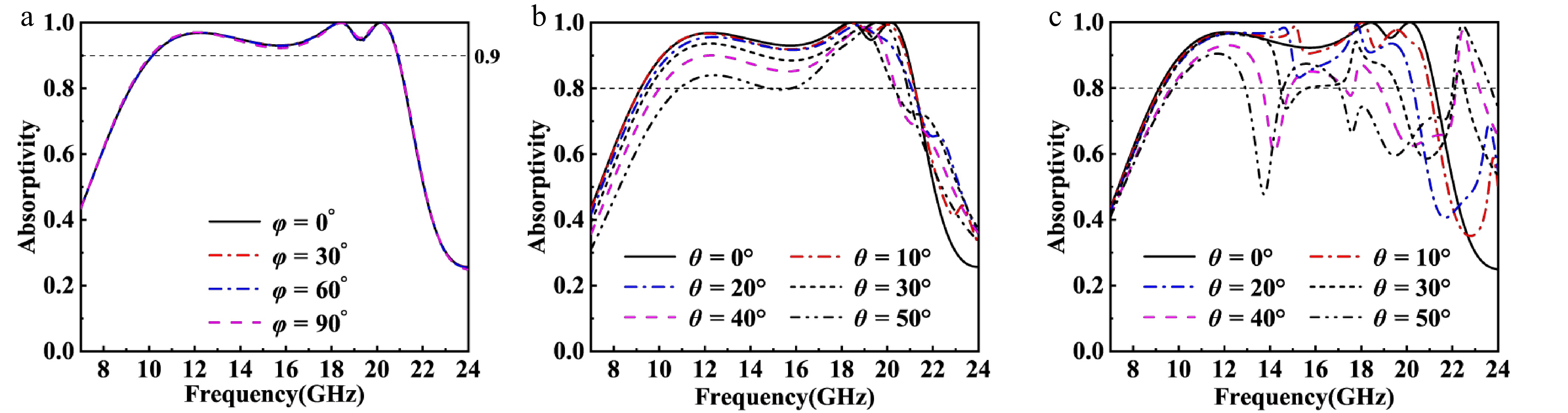
Figure 3.
Absorptivity of the absorber at different (a) polarization angles, (b) incidence angles in TE mode, and (c) incidence angles in TM mode.
Fig. 3a depicts the polarization characteristics of the absorber at 0°–90° polarization angles. It is clearly demonstrated that the absorptivity remains above 90% in the range of 10.15 to 20.91 GHz across all polarization angles, indicating excellent polarization insensitivity. All of the above analyses are performed under normal-phase incidence of the electromagnetic wave. The absorption behavior of absorbers varies with different incidence angles. Fig. 3b and c shows the absorptivity under oblique incidence in TE and TM modes, respectively. In TE mode, the overall absorption bandwidth of the absorber decreases with the increase of the incident electromagnetic wave angle. However, when the incident angle is less than 50°, the absorber maintains an absorptivity greater than 80% over the 10.86–20.88 GHz range. In the TM mode, the absorber exhibits greater sensitivity to the incident angle, with absorptivity exceeding 80% over the 9.27–19.62 GHz range.
In order to further visualize the performance of the designed absorber, Fig. 4 shows the electric field distribution in the vicinity of each of the three resonance points. The electric field distribution at 12.24 and 18.4 GHz is shown in Fig. 4a and b, respectively. It is evident that the high electric field regions are mainly distributed around chip resistors as well as at the edges and tips of the unit cells. The chip resistor causes an interruption in the electric field, resulting in strong local electric field gradients. A portion of the electromagnetic wave energy is lost through ohmic dissipation in the chip resistors. The other part of the electromagnetic wave energy loss is related to the distribution of the high electric field regions at the edges and tips of the resonant cells. In this case, the absorber undergoes localized surface resonance, leading to dielectric losses and further absorption. Fig. 4c illustrates the electric field distribution at 20.16 GHz, where the high electric field regions are mainly distributed at the tips of the resonance unit as well as at the edge position of the ring. In this case, the absorber undergoes mainly localized surface plasmon resonance, where the electromagnetic energy is captured by the locally enhanced electric field and converted into thermal energy through dielectric losses. It is the coexistence of multiple dissipation modes that provides the absorber with good broadband absorption.
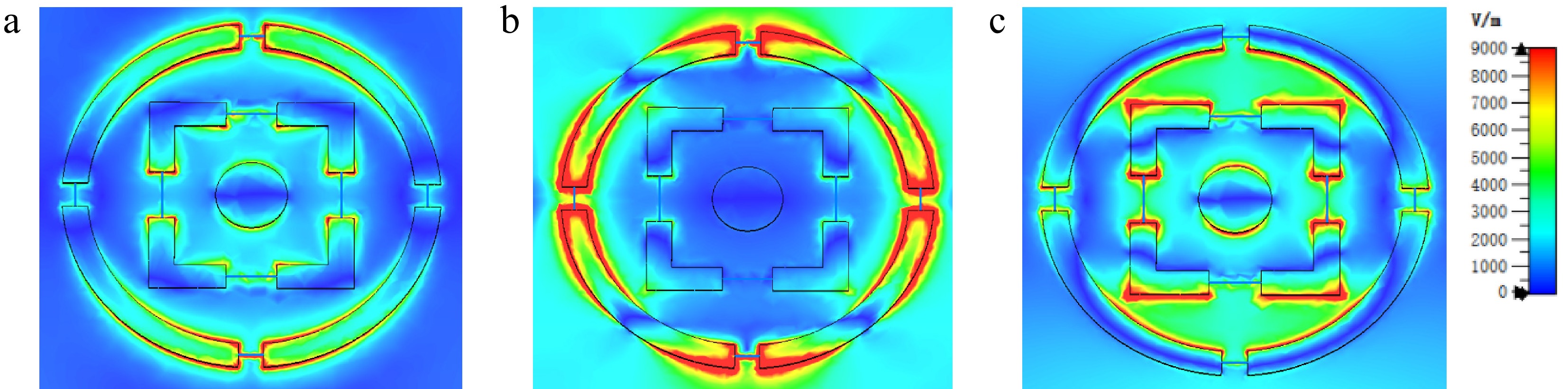
Figure 4.
Electric field distribution at three resonance frequencies. (a) 12.24 GHz, (b) 18.4 GHz, and (c) 20.16 GHz.
In addition, in order to further analyze the absorption effect of the designed absorber, the surface electric power of the absorber at the resonance frequency point was further simulated and calculated. The surface current density distribution of the absorber near the three resonance points is shown in Figs 5 and 6.
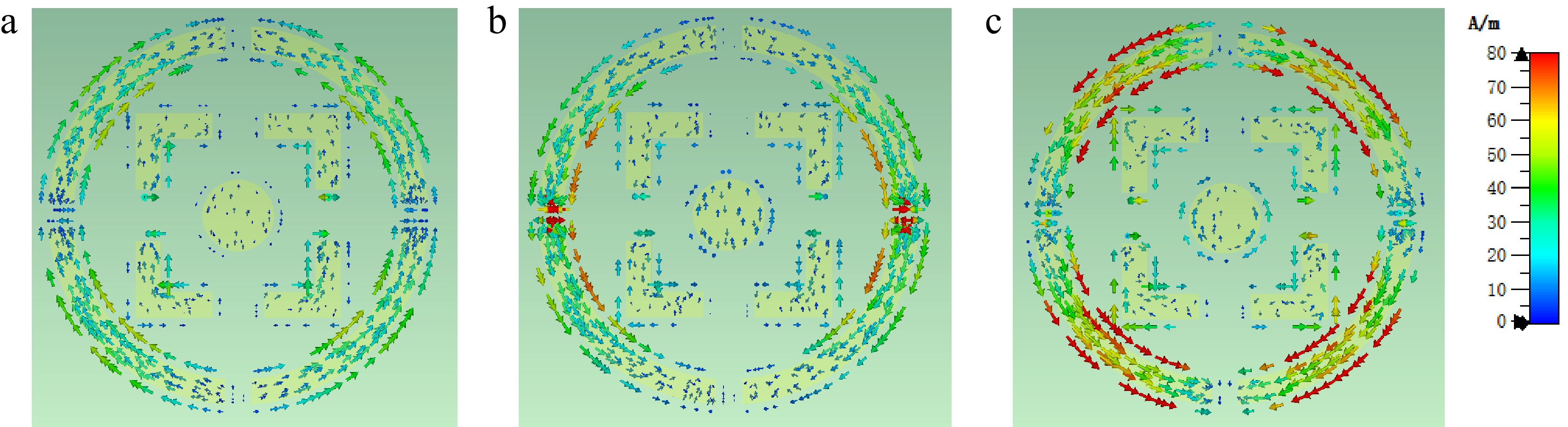
Figure 5.
The surface current density distribution (a) 12.24 GHz, (b) 18.4GHz, and (c) 20.16 GHz.
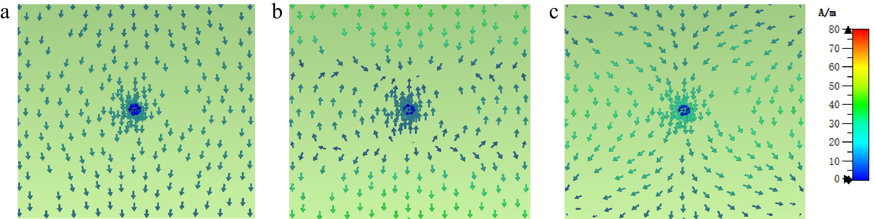
Figure 6.
The backplane current density distribution (a) 12.24 GHz, (b) 18.4 GHz, and (c) 20.16 GHz.
At 12.24 GHz, as shown in Figs 5a and 6a, the current direction of the resonant layer of the absorber is opposite to that of the metal backplate. This means that magnetic field coupling is formed in the upper and lower current loops, indicating that the main resonance mode at this frequency point is magnetic resonance. As shown in Fig. 5b and c, at 18.4 and 20.16 GHz, the current direction of the outer ring is opposite to that of the inner square ring and metal disc, thereby exciting electrical resonance on the surface metal layer. This results in new resonance peaks in the mid-frequency and high-frequency regions, which is conducive to the formation of wideband absorption, and the distance between the mid-frequency and high-frequency resonance points is relatively close. As shown in Fig. 6b, at 18.4 GHz, the surface resonant structure can be regarded as a two-dimensional metal grating, forming a guided mode resonance at this frequency point. The current in the metal backplane is divided into three regions, with the upper and lower regions carrying current upward and the middle region carrying current downward. The currents between adjacent regions remain oppositely parallel. Meanwhile, as shown in Figs 5c and 6c, the current direction on most of the metal resonant surface and the metal backplate surface is parallel. The direction of the surface current is opposite to the direction of the electric field applied by the incident electromagnetic wave, and no magnetic field coupling of closed-loop current is formed. This indicates that electrical resonance also exists at this frequency point. Additionally, due to the requirements of the electromagnetic parameter extraction work for the absorber, tiny perforations were made in the metal ground plane without affecting the absorption characteristics[23]. Consequently, the surface current on the metal backplane of the absorber accumulates around the perforations, which is considered a normal phenomenon.
-
To verify the effectiveness of the designed absorber, the physical prototype was fabricated, and its reflection coefficient was experimentally measured. Fig. 7a and b show the physical sample of the absorber and the measurement setup in a microwave anechoic chamber, respectively. A 30 × 30 cm absorber sample consisting of a 30 × 30 unit-cell array was fabricated, ensuring that most of the electromagnetic energy was confined to the sample surface. This configuration helps to reduce the diffraction deviation of electromagnetic waves and improves the reliability of the measured reflection coefficient. Chip resistors in package size 0402 are used. During testing, two horn antennas are symmetrically positioned at various angles to simulate electromagnetic wave incidence at different angles. To minimize near-field effects, the distance between the antenna and the absorber is maintained at 1.875m, as calculated using Eq. (2). Under these conditions, the reflection coefficient is measured using a vector network analyzer:
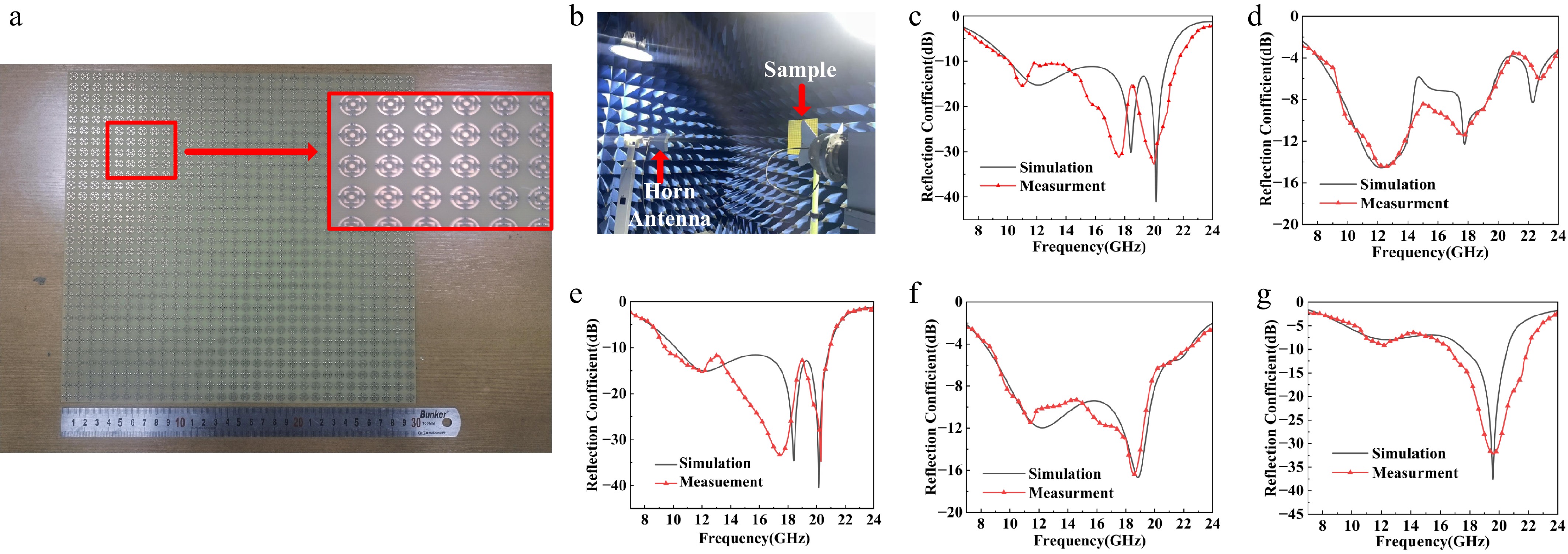
Figure 7.
Experimental tests and results; (a) absorber sample, (b) experimental setup, (c) 0° angle of incidence in TM mode, (d) 30° angle of incidence in TM mode, (e) 0° angle of incidence in TE mode, (f) 30° angle of incidence in TE mode, and (g) 50° angle of incidence in TE mode.
$ {r}_{\text{a}}=\frac{{D}^{2}}{\lambda } $ (2) where, D is the aperture of the antenna, and λ is the wavelength corresponding to the highest operating frequency of the antenna.
As shown in Fig. 7c-g, the reflection coefficients of the absorber are measured and simulated at incident angles of 0° and 30° in TM mode, and 0°, 30°, and 50° in TE mode. Minor discrepancies are observed between the measured and simulated reflection coefficients. These deviations arise due to variations in the FR-4 substrate electromagnetic properties, manufacturing tolerances, and edge effects from the finite absorber size. Experimental results validate the effectiveness of the proposed design. The comparison with other representative absorbers is shown in Table 1, demonstrating that the designed absorber exhibits favorable broadband performance and incident angle stability.
Table 1. Comparison of broadband absorbers.
Ref. Bandwidth (GHz) FBW (%) Oblique incidence Thickness (mm) Electrical thickness Structural materials Fabrication features TE TM [24] 11.4−20 54.8% 50° 50° 1.6 0.084λ0 FR-4 and metal Single layer [27] 4.3−11.1 88.3% 60° 60° 9.48 0.243λ0 PVC/ITO/OCA/PET Double-layer [28] 5.10−14.07 94% N/A N/A 6.6 0.211λ0 Rossler chaos surface Chaotic units [25] 12.35−14.65 17% 45° 45° 2 0.09λ0 FR-4 and metal Single layer [26] 8.9−14.0 44.5% 50° 60° 1.6 0.061λ0 ITO and substrate Single layer This work 10.15−20.91 69.3% 50° 30° 2.3 0.119λ0 FR-4 and metal Single layer -
In summary, this paper presents a wideband electromagnetic absorber based on a simple topology utilizing an FR-4 substrate and chip resistors, significantly reducing fabrication complexity and cost. According to Eq. (3), the absorber achieves a fractional bandwidth (FBW) of 69.3% and exhibits structural symmetry, resulting in excellent polarization insensitivity. In both TE and TM modes, the absorber maintains an absorption rate above 80% when the incidence angle is less than 50° and 30°, respectively, demonstrating robust angular stability. Experimental measurements of the reflection coefficient validate its absorption performance. Table 1 shows that the proposed unit cell uses conventional FR-4 and copper in a simple sandwich configuration, which is relatively low-cost and easy to fabricate compared with multilayer or functional-material designs. Compared with studies by Araújo et al.[24], Pham et al.[25] and Lei et al.[26], which also uses single layer, the proposed absorber achieves a wider fractional bandwidth. Compared with Jiang et al.[27] and Yuan et al.[28], the proposed absorber has a lower electrical thickness. Thus, the proposed design combines fabrication economy with broadband absorption performance and shows promising potential for applications in electromagnetic compatibility, electromagnetic shielding, and radar stealth technologies.
$ FBW=\frac{2({f}_{\max }-{f}_{\min })}{{f}_{\max }+{f}_{\min }}\times 100\text{%} $ (3) where, fmax and fmin are the upper and lower frequencies of the 90% absorption band, respectively.
-
The authors confirm their contributions to the paper as follows: conceptualization: Zhao Y, Chen T, Yang W, Zhang X; methodology, writing – original draft preparation: Zhao Y, Chen T, Yang W; principle analysis: Zhao Y, Chen T, Luan J, He H; platform construction and experimental testing: Zhao Y, Chen T, Yang W, Zhang X, Luan J, He H; funding acquisition, writing–review and editing: Chen T, Yang W, Zhang X; validation: Chen T, Yang W; project administration: Chen T, Yang W, Zhang X. All authors reviewed the results and approved the final version of the manuscript.
-
The data presented in this study are available on request from the corresponding author due to the funder's privacy policy.
-
The authors declare that they have no conflict of interest.
- Copyright: © 2026 by the author(s). Published by Maximum Academic Press, Fayetteville, GA. This article is an open access article distributed under Creative Commons Attribution License (CC BY 4.0), visit https://creativecommons.org/licenses/by/4.0/.
-
About this article
Cite this article
Zhao Y, Yang W, Chen T, Zhang X, Luan J, et al. 2026. Design of a single-layer broadband absorber based on a simple nested topology of lumped elements. Wireless Power Transfer 13: e028 doi: 10.48130/wpt-0026-0020 

Design of a single-layer broadband absorber based on a simple nested topology of lumped elements
- Received: 08 February 2026
- Revised: 02 April 2026
- Accepted: 17 April 2026
- Published online: 08 October 2026
Abstract: This paper designs a metasurface absorber with a simple nested topology of lumped elements, achieving over 90% absorptivity across the frequency range of 10.15 to 20.91 GHz, demonstrating strong polarization insensitivity, and exhibiting stability for incidence angles of up to 30° and 50° for TM and TE modes, respectively. The designed absorber features a single-layer structure and achieves excellent broadband absorption performance through the superposition of resonant peaks at three distinct frequency points. The absorber comprises an FR-4 dielectric substrate, a metallic resonant structure, eight chip resistors, and a metallic reflective backplate. The absorption performance is analyzed under varying structural parameters, and the electromagnetic wave absorption mechanism is investigated through the surface electric field distribution. Furthermore, a prototype is fabricated, and its absorption characteristics are experimentally validated. Featuring broadband absorption with simple topology, the proposed absorber demonstrates strong potential for applications in electromagnetic shielding, radar stealth, and electromagnetic compatibility.
-
Key words:
- Microwave /
- Metamaterials /
- Wave absorber /
- Broadband