-
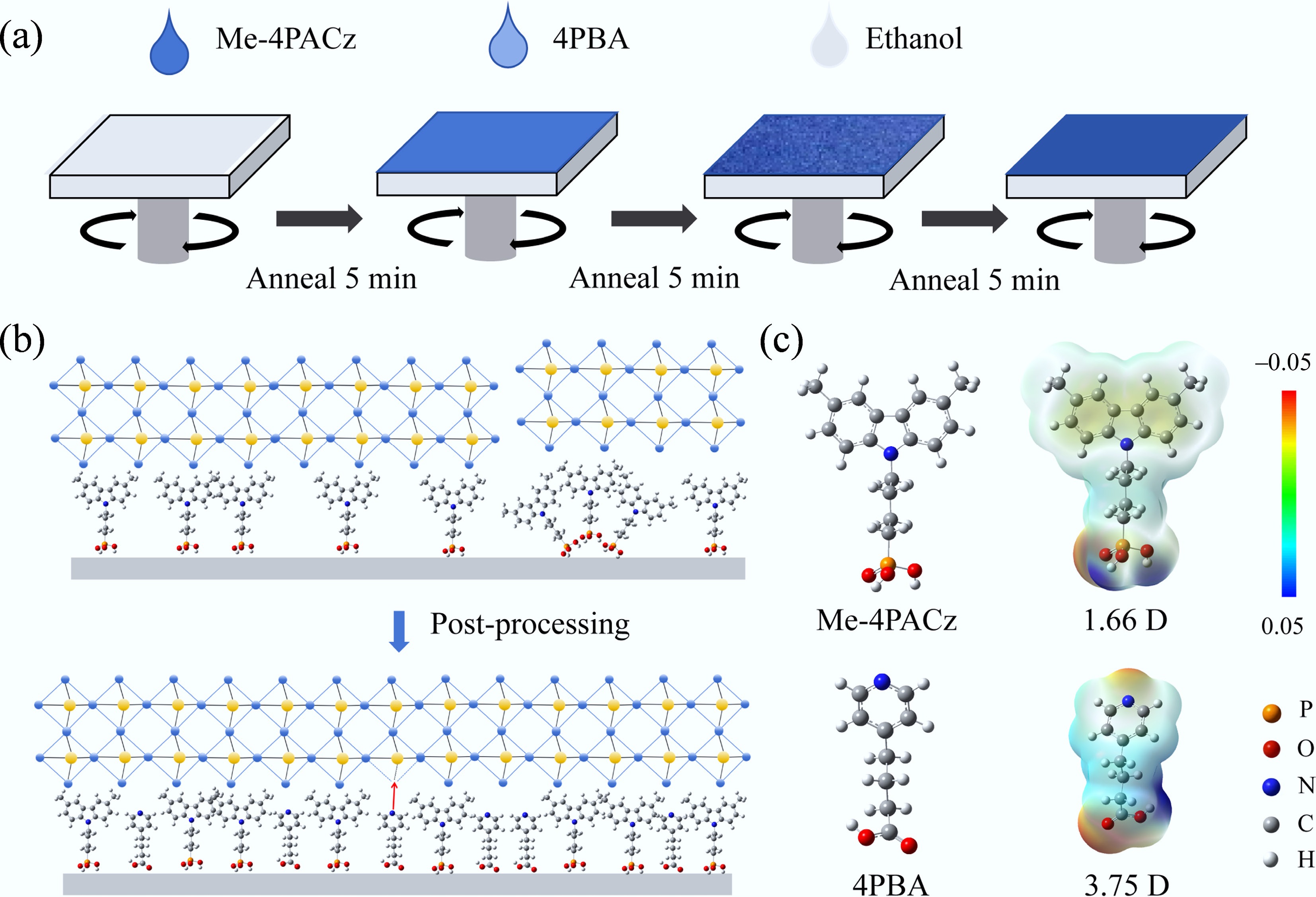
Figure 1.
(a) The schematic representation of the poSAMs deposition process; (b) the mechanism of the 4PBA post-assembly strategy; (c) the molecular structure and electrostatic potential distribution of Me-4PACz and 4PBA.
-
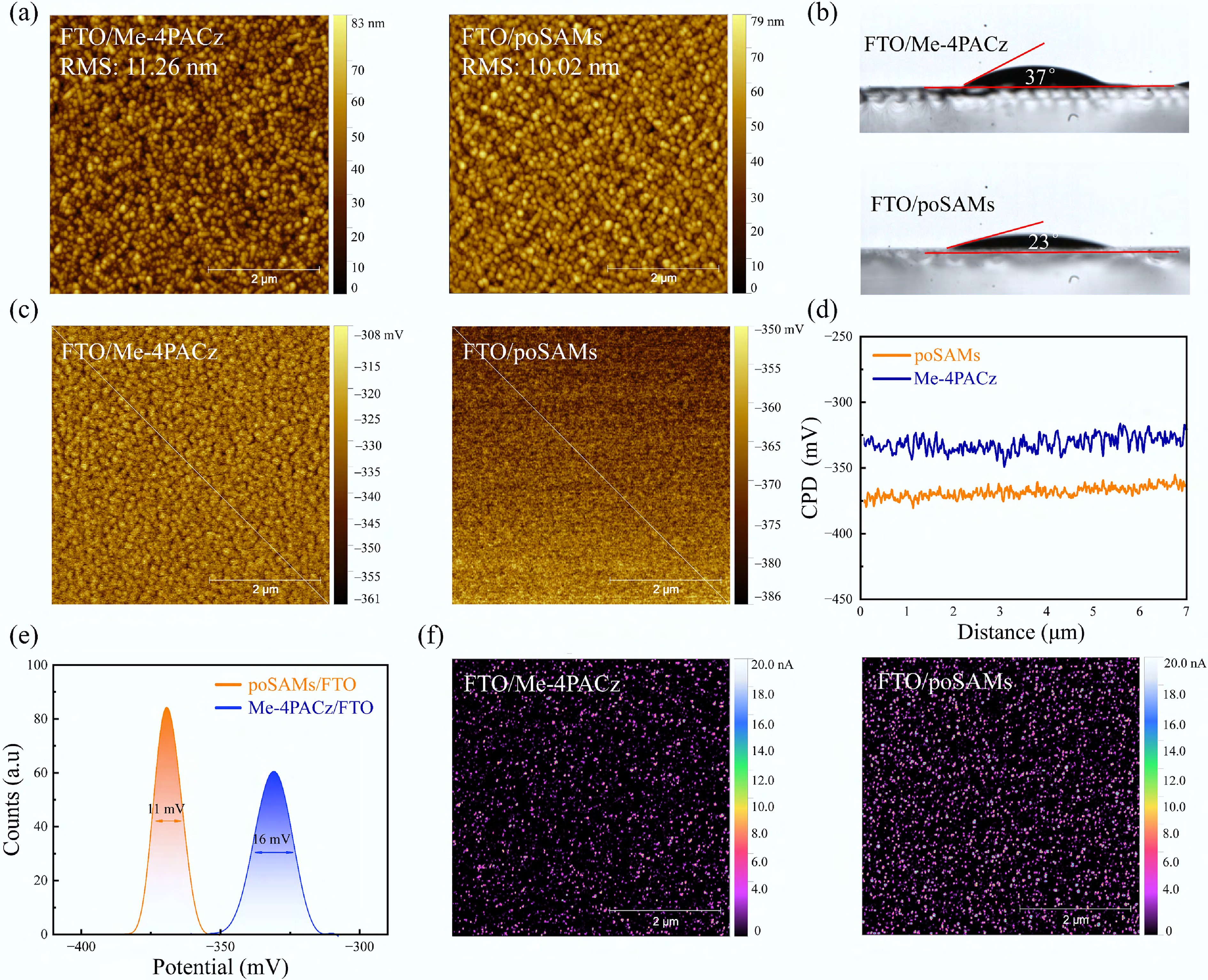
Figure 2.
(a) AFM height images of the FTO substrates covered by Me-4PACz and poSAMs; (b) contact angle of perovskite precursor with FTO/SAMs substrates; (c) KPFM images; (d) curves of FTO anchoring with SAMs, and the related (e) FWHM plot; (f) c-AFM images of Me-4PACz and poSAMs deposited on the FTO substrate.
-
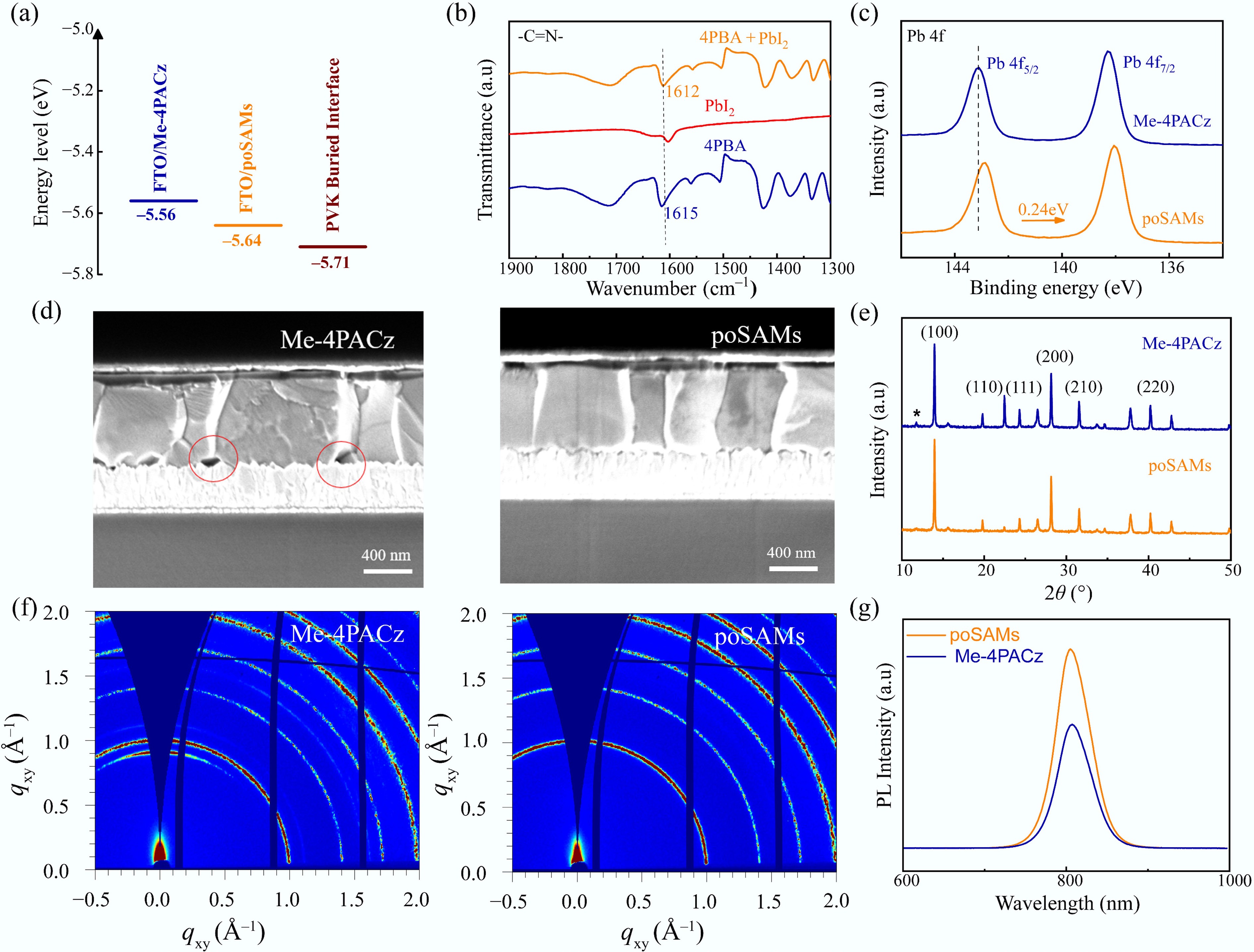
Figure 3.
(a) Energy level diagram illustrating the different SAMs and the perovskite layer; (b) FTIR analysis of 4PBA + PbI2, PbI2, and 4PBA; (c) Pb 4f regions in the XPS spectra for the perovskite films deposited on different SAM substrates; (d) cross-sectional SEM images of the device with different SAMs; (e) XRD patterns and (f) GIWAXS images of the perovskite film deposited on different SAMs substrates; (g) PL spectra of the perovskite film deposited on different SAM substrates.
-
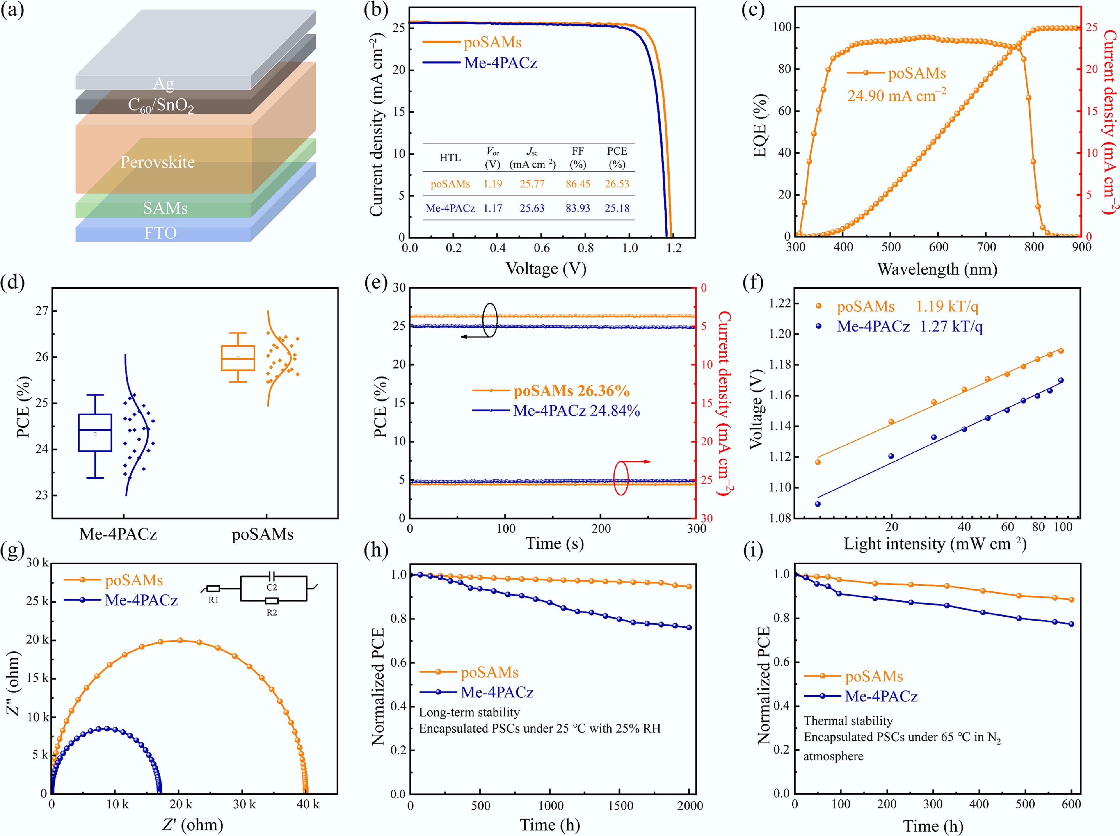
Figure 4.
(a) The architecture of the inverted device; (b) the J-V curves of Me-4PACz- and poSAMs-based PSCs; (c) the EQE spectrum of poSAMs-based PSC; (d) the statistical PCE, (e) MPP tracking; (f) Voc vs light intensity; (g) EIS of Me-4PACz and poSAMs-based PSCs; (h) long-term stability; and (i) thermal stability of encapsulated Me-4PACz and poSAMs-based devices.
Figures
(4)
Tables
(0)