


-
Electric bicycles are usually equipped with electric motors for propulsion and battery packs to power the motors. In this context, the traditional way of wired charging requires that the bike be connected directly to the charger or that the heavy on-board battery pack be removed for connection to the charger. Inductive power transfer (IPT) systems can be applied to achieve a non-contact power supply, which makes them robust to dirt, ice, water, and chemicals, thus eliminating the need for maintenance.
An excellent anti-misalignment performance plays a vitally important role in the wireless charging system for electric bicycles. At the receiving end of an electric bicycle, there is an offset of horizontal position during placement, which affects the coupling coefficient of the wireless charging system, thus reducing both output power and efficiency.
Many studies have been conducted to enhance the misalignment features of wireless power transfer (WPT) systems. For instance, a detuning compensation network has been proposed to study and enhance the misalignment performance[1]. To enhance the misalignment performance, the transmitting resonator and the receiving resonator are adjusted to be inductive and capacitive at the operating frequency, respectively[2]. Both S/SP compensation and PS/S compensation are proposed as a general method that can be used to develop the primary compensation network for dynamic WPT systems[3,4]. Utilizing this technique, a T-type compensation network has been created for dynamic WPT systems. Additionally, a primary-side X-type compensation topology for WPT systems has been proposed to achieve stable output in the presence of misalignment[5].
The methods for controlling misalignment tolerance have been thoroughly studied[6−8]. These methods usually require the use of communication devices, which tend to induce data latency. Moreover, the controllers can be disrupted by extra volume and complex control circuits.
Simplification of control strategies is possible if IPT systems can withstand misalignment. Consequently, scientists are concentrating on improving misalignment tolerance by designing magnetic pads, fine-tuning compensation settings, and creating hybrid structures. For example, double-D, dipole, tripole pads, and asymmetric magnetic couplers, have been proposed to generate a relatively uniform magnetic field[9−12]. However, some methods are applicable only when the operation is conducted with misalignment tolerance in one direction. Additionally, there is minimal focus on examining the steady output traits of these IPT systems.
A hybrid WPT system is presented to perform CC-CV output charging with a high misalignment tolerance for charging EV batteries[13]. The ZPA condition and ZVS soft switching are easily achievable throughout the charging process, even in the presence of misalignment. However, there is a high complexity in the coupling relationship of this model. The power density and system efficiency are decreased due to using multiple coils.
There are also examples of introducing DD coils and utilizing dual receivers with DD and Q coils to improve misalignment performance[14]. The DD and Q coils are inherently separated. Nonetheless, it seems improbable that a pair of receiver coils will concurrently emit the identical magnetic field produced by the DD transmitter. Another option involves using the Q coil to overlap with the DD coil, where a compact double-sided decoupled-coil-based WPT system has been proposed[15]. The suggested design suggests a more intense magnetic field on one side of this coupler compared to the other, potentially leading to magnetic saturation.
In engineering works, IPT technology is applied primarily to the battery load. During the charging process, the equivalent impedance of the battery changes constantly[16]. Also, coil misalignment can reduce its coupling coefficient, resulting in a significant deviation from the rated duty point and a decline in efficiency of the system[17]. Environmental factors such as ocean currents can lead to coupler displacement during deep-sea charging operations, while terrestrial charging systems face similar challenges when vehicular positioning errors exceed coil alignment tolerances. Therefore, the IPT system is required to achieve load-independent constant output and show strong robustness to coupling variation.
To achieve this purpose, various control methods such as phase-shift control, pulse frequency control, frequency control, and hybrid control methods have been proposed[18−21]. However, the use of complex control methods tends to increase the overall system cost and power loss. In addition, the stability of the control system can be affected by the speed and accuracy of data transmission.
Reconfigurable topology provides another solution to achieving the strong tolerance of misalignment. A reconfigurable series–series (SS) topology is presented to ensure the stability of output in the presence of significant coupling variation. However, low efficiency results from using a large number of composition components. To minimize the number of composition components used, a reconfigurable rectifier-based detuned SS topology is presented[22]. Nevertheless, the use of detectors and controllers is required to enable the reconfiguration, which remains an issue with the control strategy.
A bicycle inductive power transfer system should meet the following requirements. one is to achieve misalignment tolerance in x- and y-directions; another is to improve battery life through CC and CV charging; the last one is a high power density of the system to meet the requirements for high integration and efficiency.
This paper aims to address the aforementioned problems by developing a wireless charging system with high misalignment tolerance and load-independent output. The secondary side utilizes thin magnetic materials without aluminium shielding. Furthermore, in the actual experimental process, the reconfigurable topology and related control circuits are integrated into the secondary side coil in order to further reduce the weight of the receiving end. According to the results of the JMAG simulation and experiment, the proposed model and the topology are effective. To be specific, the prototype output power reaches 200 W with a maximum efficiency of 92.7%.
-
The coil structure presented in this paper is in reverse parallel with the third coil on the secondary side, with a single coil on the primary side. The equivalent model of the coil is shown in Fig. 1.
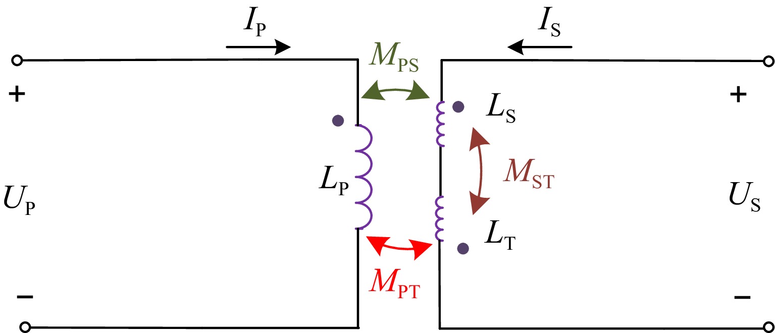
Figure 1.
Equivalent circuit of the proposed coil.
The secondary side coil current Is inflow from the secondary side coil Ls and exits through the third coil. LT. LP, LS, and LT are inductances of the primary, secondary, and auxiliary coils of the loosely coupled transformer. UP, US, IP, and IS represent the input/output voltage and current of the coupler. MPT, MPS, and MTS are the relevant coupling coefficients of the primary coil, secondary coil, and additional coil. According to the M model and Kirchhoff's law as shown in Fig. 2, it can be indicated that:
$ \left[\begin{array}{l}{\dot{U}}_{P}\\ {\dot{U}}_{S}\end{array}\right]=\left[\begin{array}{l}j\omega {L}_{P}\\ j\omega ({M}_{PS}-{M}_{TS})\end{array}\begin{array}{l}j\omega ({M}_{PS}-{M}_{TS})\\ j\omega ({L}_{S}+{L}_{T}-2{M}_{PT})\end{array}\right]\left[\begin{array}{l}{\dot{I}}_{P}\\ {\dot{I}}_{S}\end{array}\right] $ (1) 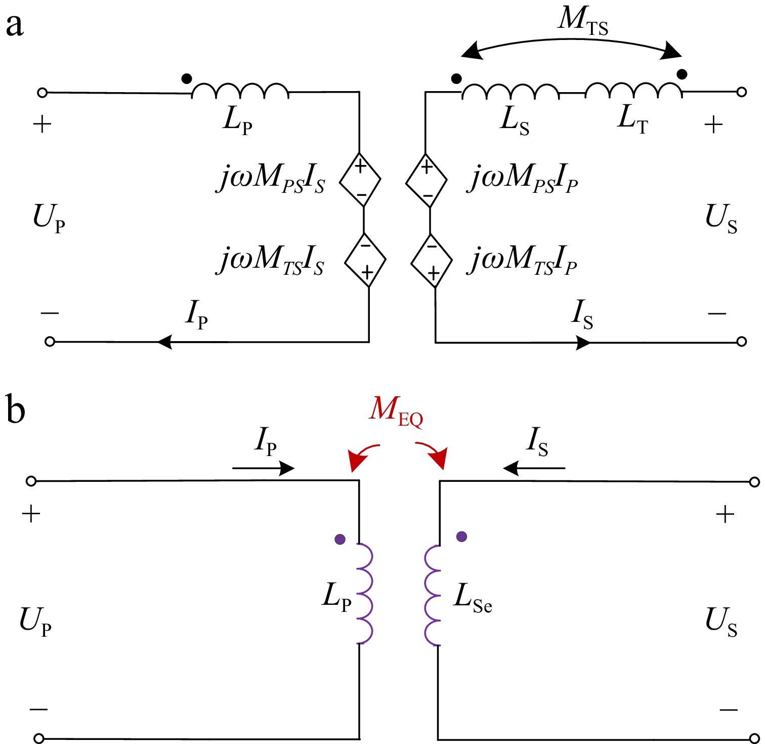
Figure 2.
M model and equivalent model of the proposed coil. (a) M model. (b) Equivalent model.
For convenience of analysis, the secondary side coil LS and auxiliary coil LT can be equivalent to one coil MEQ. The relationship between self-inductance and mutual inductance in Fig. 3 is shown as follows:
$ L_{_P}^{'} = {L_P} + {L_T} - 2{M_{PT}} $ (2) $ {M_{EQ}} = {M_{PS}} - {M_{PT}} $ (3) 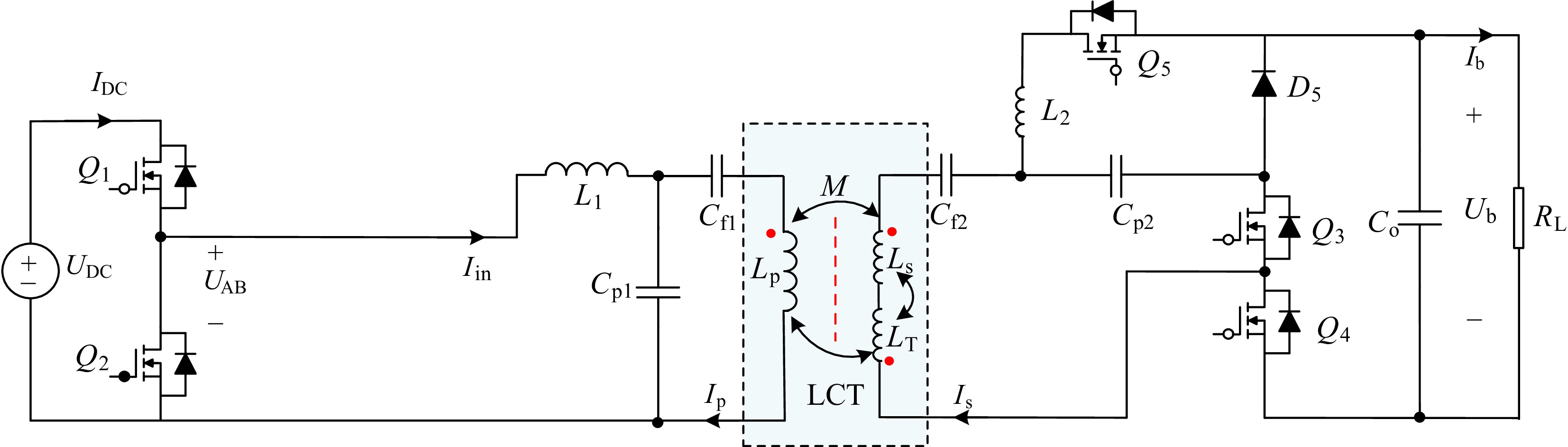
Figure 3.
Circuit diagram of the proposed system.
MPS and MPT are reduced simultaneously under the misalignment condition. The degree of reduction of the two mutual inductances is expressed as ΔMPS and ΔMPT. The equivalent mutual inductance coefficient can be expressed as:
$ \begin{aligned} M_{_{EQ}}^{'}& = ({M_{PS}} - \Delta {M_{PS}}) - ({M_{TS}} - \Delta {M_{TS}}) \\ & = {M_{EQ}} - (\Delta {M_{PS}} - \Delta {M_{TS}}) \end{aligned} $ (4) Assuming that ΔMPS = ΔMPT, then
$ M_{EQ}^{'}=M_{EQ} $ -
The circuit diagram of the proposed system is shown in Fig. 3. UAB and Iin are the AC output voltage and current of the half-bridge inverter, and Uab and Iab represent the AC input voltage and current of the rectifier. UDC and IDC represent the DC input voltage and current of the half-bridge inverter, and Ub and Ib are the DC output voltage and current of the rectifier. The high-order compensation networks LCC, composed of L1, Cp1, Cf1, and L2, Cp2, Cf2 are applied on the primary and secondary sides, respectively.
When the topology operates in CV mode, switch Q4 is turned ON, and Q3 and Q5 are turned OFF, constructing LCC-S topology. The AC-DC rectifier is realized by a half-bridge on the secondary side. The reconfigurable topology and equivalent circuit for CV mode are presented in Figs 4 and 5. For Fig. 4, the current flows through freewheeling diode of Q4 and diode D6.
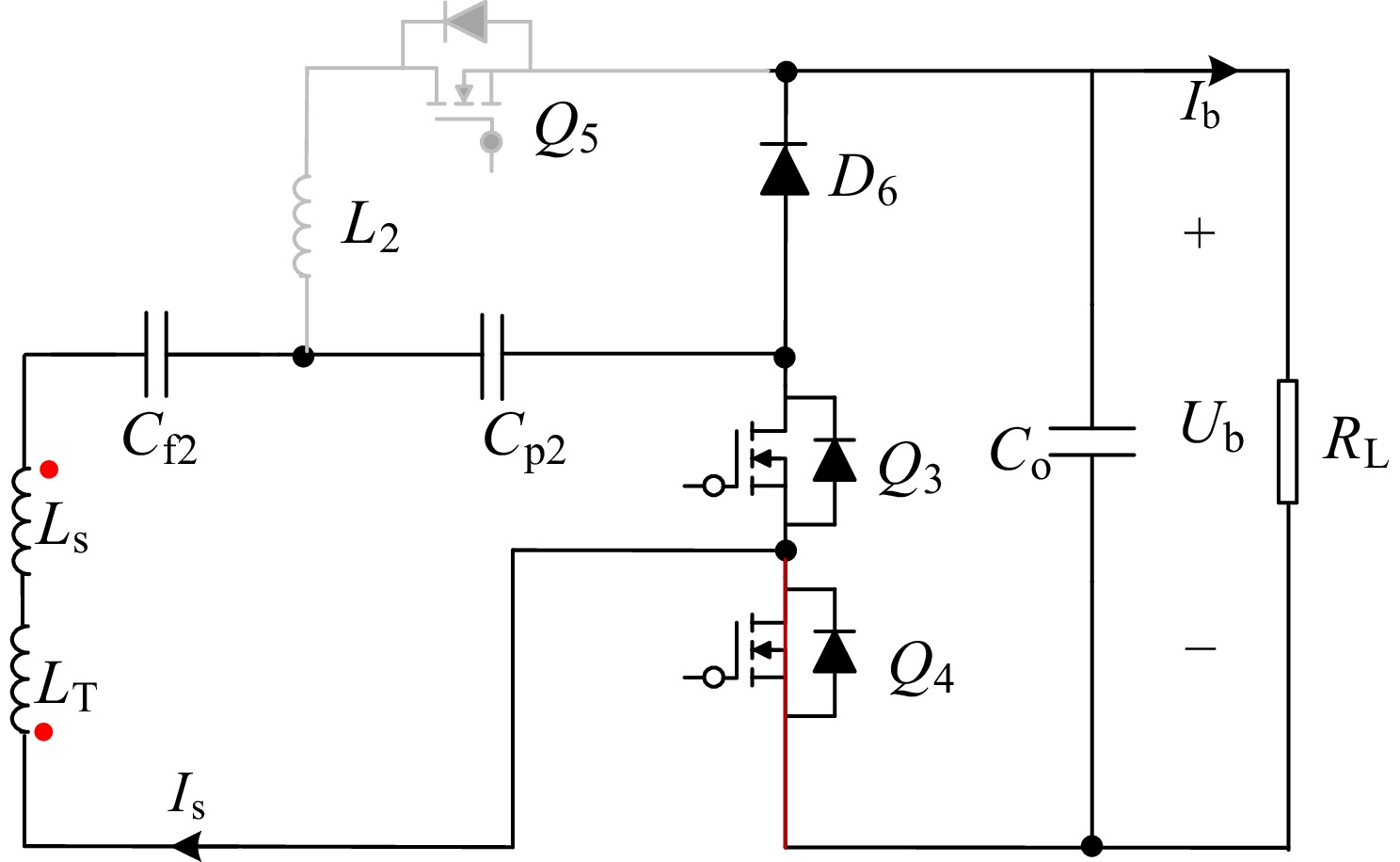
Figure 4.
Equivalent circuit in CV mode.
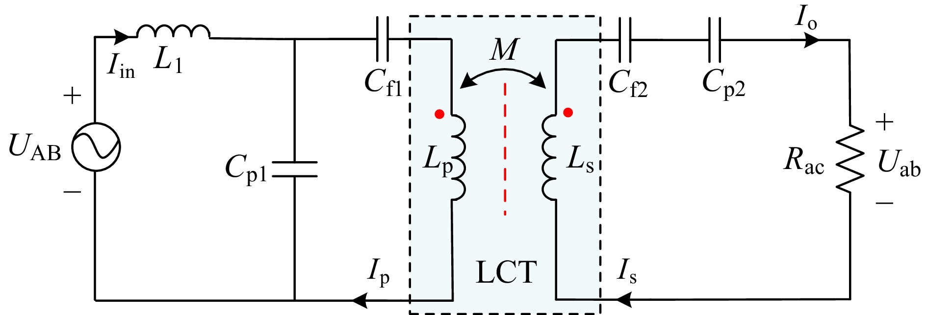
Figure 5.
Equivalent resonant network in CV mode.
The Kirchhoff's law-based formula for the AC input current is:
$ {I_{{\mathrm{in}}}} = \dfrac{{{U_{{\mathrm{AB}}}}}}{{{Z_{{\mathrm{in}}}}}} = \dfrac{{{U_{{\mathrm{AB}}}}M_{EQ}^2}}{{{L_1}^2{R_{{\mathrm{ac}}}}}} $ (5) The AC output voltage and voltage gain ratio can be determined as:
$ \left\{ \begin{gathered} {U_{{\mathrm{ab}}}} = {I_{\mathrm{s}}}{R_{{\mathrm{ac}}}} = \dfrac{{{M_{{\mathrm{EQ}}}}{U_{{\mathrm{AB}}}}}}{{{L_1}}} \\ {G_{\mathrm{V}}} = \left| {\dfrac{{{U_{{\mathrm{ab}}}}}}{{{U_{{\mathrm{AB}}}}}}} \right| = \dfrac{{{M_{{\mathrm{EQ}}}}}}{{{L_1}}} \\ \end{gathered} \right. $ (6) The current on the primary and secondary side coils is derived as:
$ \left\{ \begin{gathered} {I_{\mathrm{p}}} = \dfrac{{{R_{{\mathrm{ac}}}}{U_{{\mathrm{AB}}}}}}{{{{({\omega _0}{M_{{\mathrm{EQ}}}})}^2}}} \\ {I_{\mathrm{s}}} = \dfrac{{{M_{{\mathrm{EQ}}}}{U_{{\mathrm{AB}}}}}}{{{L_1}{R_{{\mathrm{ac}}}}}} \\ \end{gathered} \right. $ (7) The DC output voltage and current can be calculated as:
$ \left\{ \begin{gathered} {I_{\mathrm{b}}} = \dfrac{1}{2}\dfrac{{{M_{{\mathrm{EQ}}}}{U_{{\mathrm{AB}}}}}}{{{L_1}{R_{\mathrm{L}}}}} \\ {U_{\mathrm{b}}} = \dfrac{1}{2}\dfrac{{{M_{{\mathrm{EQ}}}}}}{{{L_1}}}{U_{{\mathrm{AB}}}} \\ \end{gathered} \right. $ (8) The input and output voltage and current relationship is given as:
$ \left\{ \begin{gathered} {U_{{\mathrm{AB}}}} = \dfrac{{\sqrt 2 {U_{{\mathrm{DC}}}}}}{\pi } \\ {I_{{\mathrm{in}}}} = \dfrac{{\sqrt 2 {I_{{\mathrm{DC}}}}}}{\pi } \\ \end{gathered} \right. $ (9) $ \left\{ \begin{gathered} {U_{\mathrm{b}}} = \dfrac{{\sqrt 2 {U_{{\mathrm{ab}}}}}}{\pi } \\ {I_{\mathrm{b}}} = \dfrac{{\pi {I_{{\mathrm{ab}}}}}}{{\sqrt 2 }} \\ \end{gathered} \right. $ (10) The relationship of AC and DC resistance is calculated as:
$ {R_{{\mathrm{ac}}}} = \dfrac{2}{{{\pi ^2}}}{R_{\mathrm{L}}} $ (11) The calculated AC-AC efficiency can be derived as:
$ \eta = \dfrac{{I_{_{\mathrm{S}}}^2{R_{{\mathrm{ac}}}}}}{{I_{_{\mathrm{S}}}^2{R_{{\mathrm{ac}}}} + I_{{\mathrm{in}}}^2{R_{{\mathrm{L}}1}} + I_{\mathrm{p}}^2{R_{\mathrm{p}}} + I_{\mathrm{S}}^2{R_{\mathrm{S}}}}} = \dfrac{1}{{1 + \dfrac{{{R_{\mathrm{S}}}}}{{{R_{{\mathrm{ac}}}}}} + \dfrac{{{R_{\mathrm{p}}}{R_{{\mathrm{ac}}}}}}{{{{({\omega _0}{M_{{\mathrm{EQ}}}})}^2}}} + {{\left(\dfrac{{{M_{{\mathrm{EQ}}}}}}{{{L_1}}}\right)}^2}\dfrac{{{R_{{\mathrm{L}}1}}}}{{{R_{{\mathrm{ac}}}}}}}} $ (12) The optimal AC resistance is obtained by derivation as:
$ {R_{{\mathrm{ac}}}} = \sqrt {\dfrac{{{R_{\mathrm{S}}} + {{\left(\dfrac{M}{{{L_1}}}\right)}^2}{R_{{\mathrm{L}}1}}}}{{{R_{\mathrm{p}}}}}} {\omega _0}{M_{{\mathrm{EQ}}}} $ (13) When the topology operates in CC mode, switches Q3 and Q5 are turned ON, and Q4 is turned OFF, forming the LCC-LCC topology. The AC-DC rectifier is realized by a half-bridge on the secondary side. The reconfigurable topology and equivalent circuit for CC mode are presented in Figs 6 and 7. For Fig. 6; the current flows through the freewheeling diode of Q4 and diode D6.
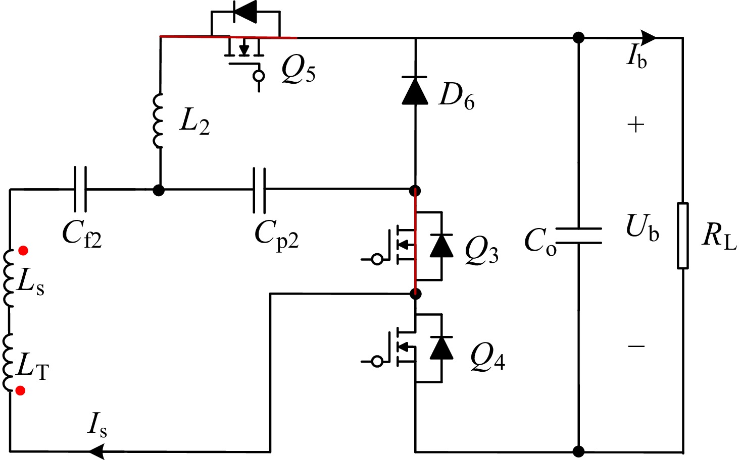
Figure 6.
Equivalent circuit in CC mode.
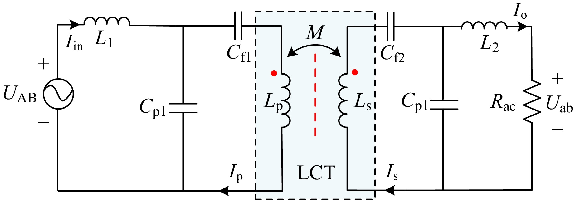
Figure 7.
Equivalent circuit of the proposed IPT system in CC mode.
The resonant conditions of the LCC-LCC topology can be given as:
$ \begin{gathered} \omega _0^2{L_1}{C_{P1}} = \omega _0^2{L_2}{C_{P2}} = 1 \\ \omega _0^2({L_P} - {L_1}){C_{f1}} = \omega _0^2({L_P} - {L_2}){C_{f2}} = 1 \\ \end{gathered} $ (14) The AC input and output current can be calculated as:
$ \left\{ \begin{gathered} {I_{{\mathrm{in}}}} = \dfrac{{{U_{{\mathrm{AB}}}}{M^2}{R_{{\mathrm{ac}}}}}}{{\omega _0^2{{\mathrm{L}}_1}^2{{\mathrm{L}}_2}^2}} \\ {I_{\mathrm{o}}} = \dfrac{{M{U_{{\mathrm{AB}}}}}}{{{\omega _0}{L_1}{L_2}}} \\ \end{gathered} \right. $ (15) The current on the primary side and secondary side coils is expressed as:
$ \left\{ \begin{gathered} {I_{\mathrm{P}}} = \dfrac{{{U_{{\mathrm{AB}}}}}}{{{\omega _0}{L_1}}} \\ {I_{\mathrm{S}}} = \dfrac{{M{U_{{\mathrm{AB}}}}{R_{{\mathrm{ac}}}}}}{{\omega _{_0}^2{L_1}L_2^2}} \\ \end{gathered} \right. $ (16) The AC output current and voltage are given as:
$ \left\{ \begin{gathered} {I_{\mathrm{o}}} = \dfrac{{{M_{{\mathrm{EQ}}}}{U_{{\mathrm{AB}}}}}}{{{\omega _0}{L_1}{L_2}}} \\ {U_{\mathrm{o}}} = \dfrac{{M{U_{{\mathrm{AB}}}}{R_{{\mathrm{ac}}}}}}{{{\omega _0}{L_1}{L_2}}} \\ \end{gathered} \right. $ (17) The DC output current and voltage are given as:
$ \left\{ \begin{gathered} {I_{\mathrm{b}}} = \dfrac{{\pi {M_{{\mathrm{EQ}}}}{U_{{\mathrm{AB}}}}}}{{\sqrt 2 {\omega _0}{L_1}{L_2}}} \\ {U_{\mathrm{b}}} = \dfrac{{\sqrt 2 {M_{{\mathrm{EQ}}}}{U_{{\mathrm{AB}}}}{R_{{\mathrm{ac}}}}}}{{\pi {\omega _0}{L_1}{L_2}}} \\ \end{gathered} \right. $ (18) The output power can be calculated as:
$ {P_{{\mathrm{in}}}} = {P_{_{\mathrm{O}}}} = \dfrac{{U_{_{{\mathrm{AB}}}}^2M_{{\mathrm{EQ}}}^2{R_{{\mathrm{ac}}}}}}{{\omega _0^2{L_1}^2{L_2}^2}} $ (19) The calculated AC-AC efficiency can be derived as:
$ \eta = \dfrac{{I_s^2{R_{{\mathrm{ac}}}}}}{{I_{_{\mathrm{S}}}^2{R_{{\mathrm{ac}}}} + I_{{\mathrm{in}}}^2{R_{{\mathrm{L}}1}} + I_{\mathrm{p}}^2{R_{\mathrm{p}}} + I_{\mathrm{S}}^2{R_{\mathrm{S}}}}} = \dfrac{1}{{1 + \dfrac{{{R_{{\mathrm{L}}1}}}}{{{R_{{\mathrm{ac}}}}}}{{\left(\dfrac{M}{{{L_1}}}\right)}^2} + \dfrac{{{R_{\mathrm{p}}}\omega _{_0}^2L_2^4}}{{R_{{\mathrm{ac}}}^3M_{^{{\mathrm{EQ}}}}^2}} + \dfrac{{{R_{\mathrm{S}}}}}{{{R_{{\mathrm{ac}}}}}}}} $ (20) The optimal AC resistance is obtained by derivation as:
$ {R_{{\mathrm{ac}}}} = \sqrt {\dfrac{{3{M^2}{R_{\mathrm{p}}}\omega _0^2L_1^4L_2^4}}{{M_{^{{\mathrm{EQ}}}}^6L_1^2{R_{{\mathrm{L}}1}} + {R_{\mathrm{S}}}M_{^{{\mathrm{EQ}}}}^4L_1^4}}} $ (21) -
As shown in Fig. 8, when the position is offset, the amplitude of change in the self-inductance of the single coil on the primary side is greater than on the secondary side, especially given a narrower air gap. It can be seen from Fig. 9 that in CC and CV modes, changes in the self-inductance value of the primary coil will not affect the current and voltage gains. Moreover, the input phase angle increases as the self-inductance value decreases, which will cause the input impedance of the system to exhibit inductive drift, causing the MOSFETs to operate under ZVS conditions. However, changes in the self-inductance value of the secondary side coil can have a significant impact on the current and voltage gains. Changes in the self-inductance value of the secondary side coil can significantly affect the magnitude of the current gain. In addition, the reduction in self-inductance value will cause the input impedance of the system to exhibit capacitive drift, thereby affecting the inverter's ability to achieve ZVS. Therefore, the third coil on the secondary side is more significant to the design of the compensation network at the receiving end, and the misalignment performance is also improved.
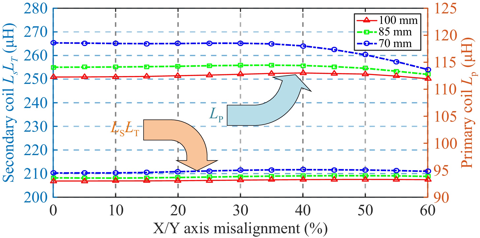
Figure 8.
Self-inductance change of the proposed three-coil structure.
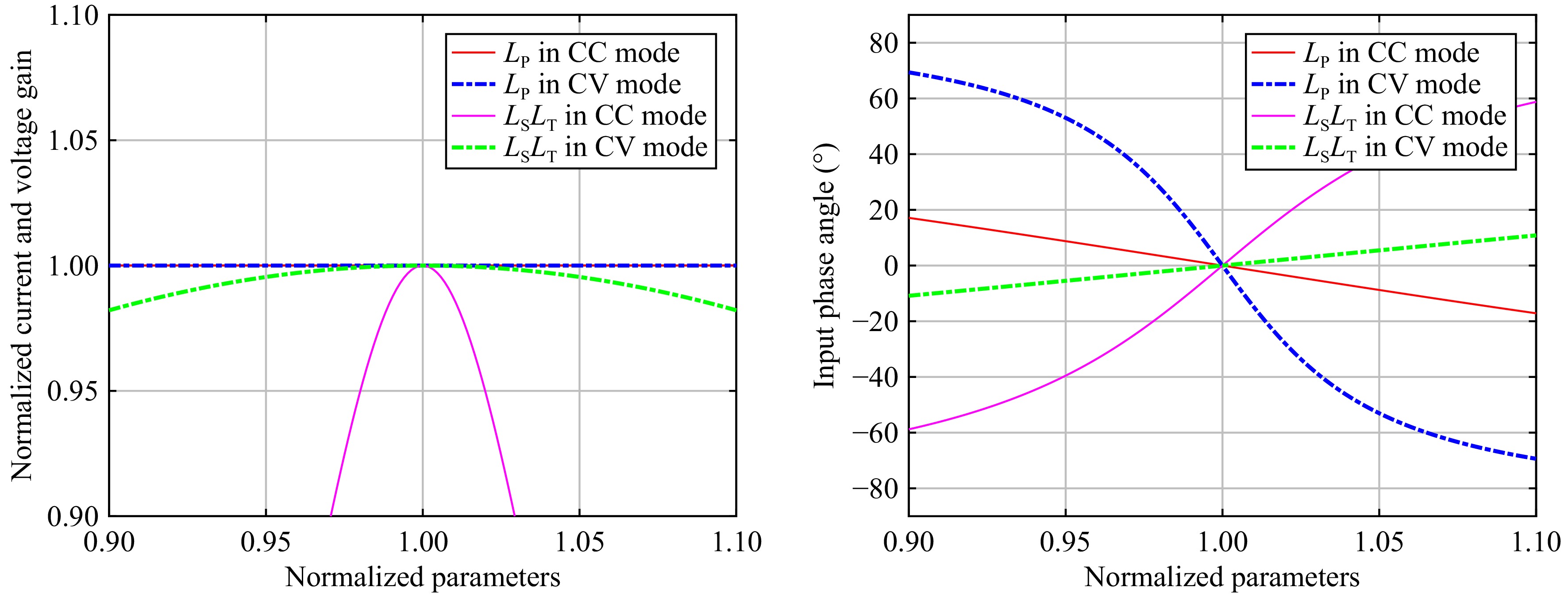
Figure 9.
Relationship curves between the normalized current/voltage gain and input phase angle with the normalized self-inductance value in CC mode and CV mode.
Figure 3 illustrates the circuit configuration of the proposed system, which consists of the three-coil magnetic coupling mechanism and reconfiguration rectifier topology. In this system, communication is not required between the primary and secondary sides. Based on the physical demand for electric bicycles, the third coil structure (LP : LS : LT) was designed as 240:250:160 mm to ensure that the constructed LCT exhibited effective misalignment tolerance capability in the x and y directions. In addition, the third coil effectively reduces the self-inductance variation under the misalignment condition on the secondary side. It should be noted that the designed LCT was not shielded with aluminium due to the low charging power of the electric bicycle.
The geometric configuration of electromagnetic couplers and their resonant frequency f0 in IPT systems is predominantly governed by structural constraints and environmental deployment conditions, necessitating the predefinition of f0 during initial parameter configuration. In the meantime, the radius R(P), the turns np, and the radius R(S), the number of turns nS, nT, are also decided by the application scenarios. Similarly, the wire diameter of Litz wire, the distance of the air gap, and the permeability, conductivity, thickness, length, and width of the ferrite core can be set according to actual needs. Magnetic ferrite was added to the primary side in order to reduce the weight of the receiving side. The design flowchart of the coupler is given in Fig. 10. The flowchart of design for the entire IPT system is shown in Fig. 11. Firstly, the initial parameter values are set based on input/output and magnetic coupling parameters, such as operating frequency and the maximum misalignment distance value. Secondly, the three coils are designed according to the study by Li et al. [23]. Thirdly, the resonant network and reconfigurable CC-CV charging topology are designed on the basis of component current and voltage stress and input/output parameters.
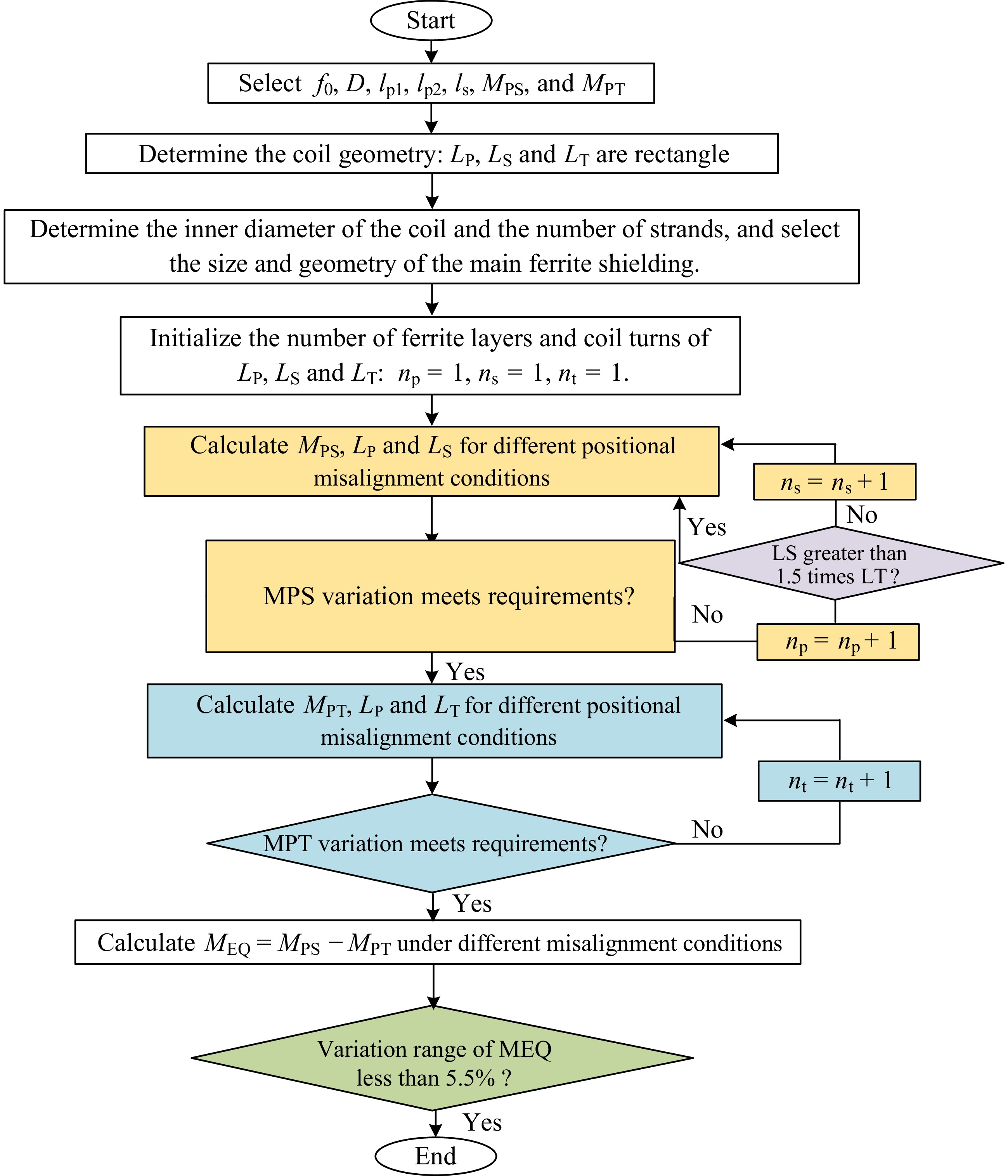
Figure 10.
Flow chart of the proposed coupler.
Figure 11.
Flow chart of the proposed IPT system.
-
Initially, a 200 W experimental prototype is built and tested to evaluate its performance, as presented in Fig. 12. According to Tables 1 and 2, the proposed IPT system shows essential characteristics and resonant network parameters, with DSP as the main controller. The air gap is 100 mm on the primary side and secondary side of the coil. The dimensions of the primary coil and secondary coil are 250 mm × 250 mm and 240 mm × 240 mm, respectively. The JMAG simulation model is shown in Fig. 13. The designed dimensional parameters of the proposed third-coil structure are listed in Table 3. In the actual experimental process, the reconfigurable topology and related control circuits are integrated into the secondary side coil in order to further reduce the weight of the receiving side.
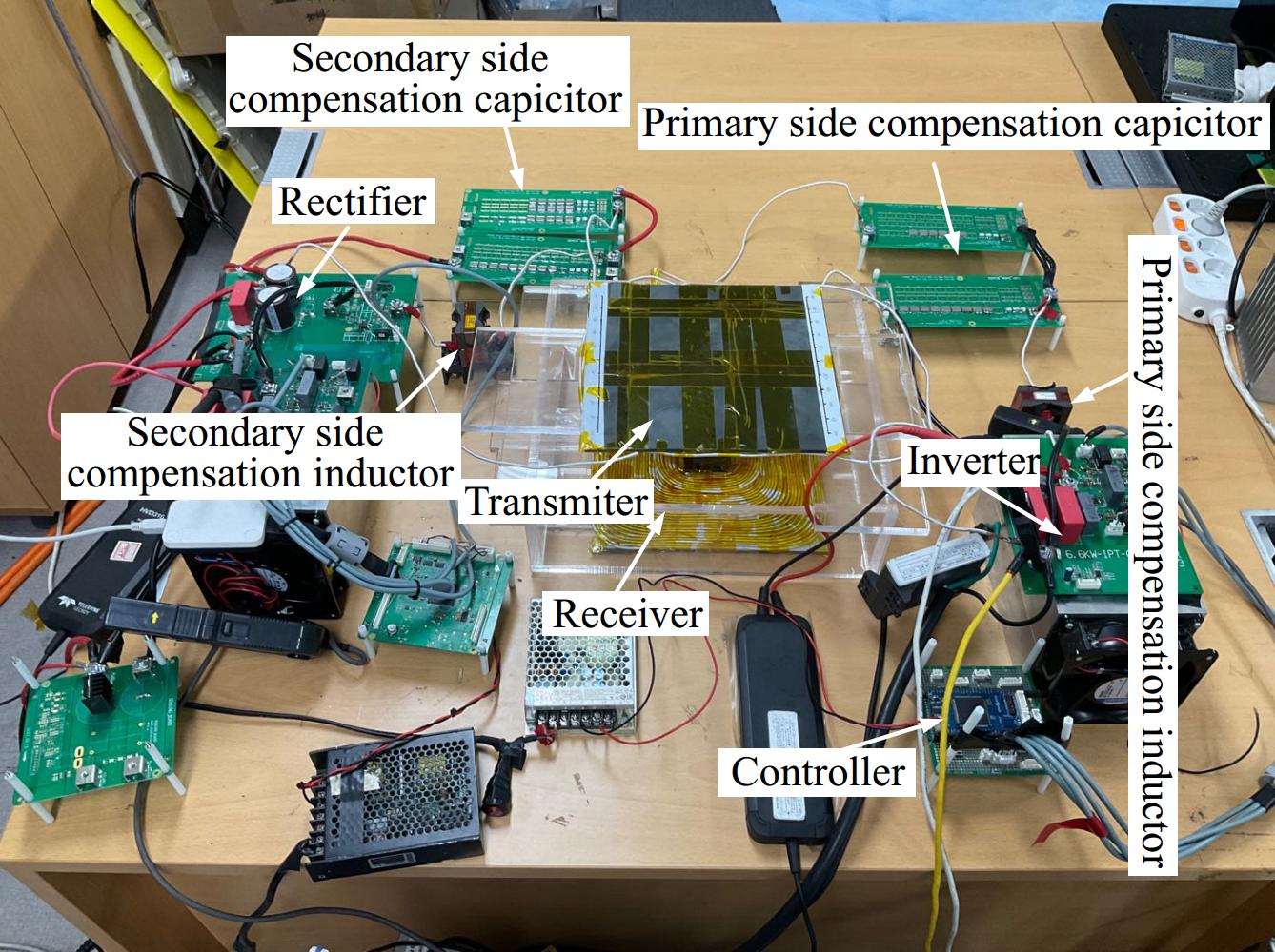
Figure 12.
Experiment setup.
Table 1. Essential system parameters of proposed IPT system.
Symbols Parameters Values UDC-link DC-link input voltage 120 V fo Resonant frequency 85 kHz Po Rate output power 200 W Uo Battery charging voltage 80 V Io Battery charging current 2.5 A k Coupling coefficient 0.073~0.122 LP Primary coil inductance 250.9 μH LS Secondary coil 161.1 μH LT Third coil 106.1 μH MPT MI between LP and LT 16.69 μH MPS MI between LP and LS 27.85 μH MTS MI between LT and LS 87.1 μH RLp Transmitting-coil AC resistance of Lp 221.03 mΩ RLs Transmitting-coil AC resistance of Ls 153.26 mΩ RLT Receiving-coil AC resistance of LT 37.75 mΩ RL1 Resistance of inductance L1 50.8 mΩ RL2 Resistance of inductance L2 62.9 mΩ RCp1 Resistance of capacitor Cp1 13.3 mΩ RCp2 Resistance of capacitor Cp2 13.7 mΩ RCf1 Resistance of capacitor Cf1 5.4 mΩ RCf2 Resistance of capacitor Cf2 4.8 mΩ rCF Turn ON-state resistance of the diodes 4.6 mΩ Rds(on) The drain-source on-state resistance 39 mΩ Table 2. Parameters of the resonant network.
Parameter Value L1 16.54 μH L2 16.53 μH CP1 212 nF Cf1 13.97 nF CP2 212 nF Cf2 45.85 nF Table 3. Essential parameters of the proposed coils.
Symbol Parameter value LP Length × width 240 mm × 240 mm LT Length × width 160 mm × 160 mm LS Length × width 250 mm × 250 mm Dd Inside radius (LS) 50 mm nP Turns (LP) 27 nS Turns (LS) 18 nT Turns (LT) 16 R(P) Transmitting coil dimension 240 mm × 240 mm × 2.5 mm R(S) Receiving coil dimension 250 mm × 240 mm × 5 mm 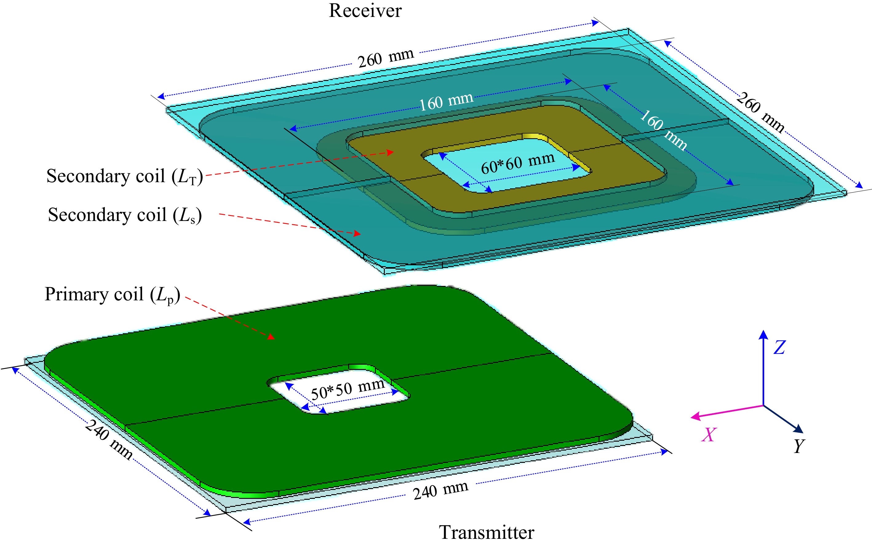
Figure 13.
JMAG simulation model.
Performance of the proposed IPT charger
-
Figure 13 depicts the magnetic field distribution under alignment and misalignment conditions. In Fig. 14a, the magnetic flux density is displayed when distance is set to 90 mm under the alignment conditions. The proposed third-coil structure design is beneficial to improve the anti-misalignment capability in the horizontal direction. Figure 14b illustrates the magnetic flux density when the receiver undergoes a horizontal movement of 100 mm, while distance remained constant. It is evident from Fig. 14b that the magnetic field density distribution is slightly weakened but remains relatively uniform, indicating that Meq can remain constant after misalignment occurs.
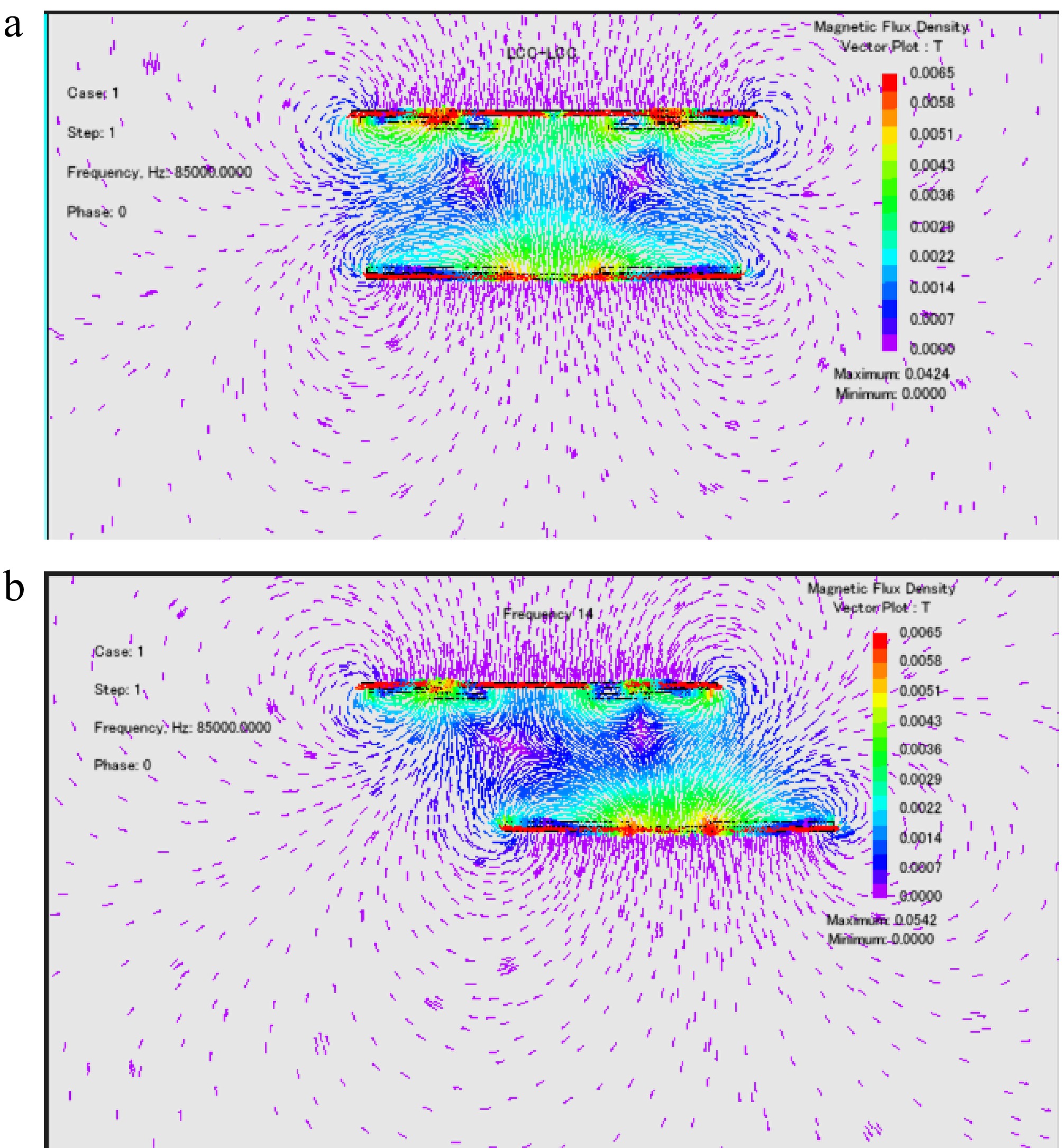
Figure 14.
Simulated magnetic flux density under (a) alignment. (b) X- or Y-axis misalignment with 42% deviation.
Figure 15 shows the experimental waveform of the input/output voltage and current for the resonant network under the CC condition. The inverter includes a zero phase angle (ZPA) condition which aligns with the theoretical analysis. An example of an experimental waveform of the half-bridge inverter and rectifier under the CC condition is shown. Figure 16 shows the DC output characteristics as the load varies. Apparently, when the DC resistance increases from 18 to 32 Ω, the DC output power rises from 110 to 200 W, the output voltage increases from 44 V to 80 V, and the output current remains 2.5 A. The maximum fluctuation of system output current is 3%.
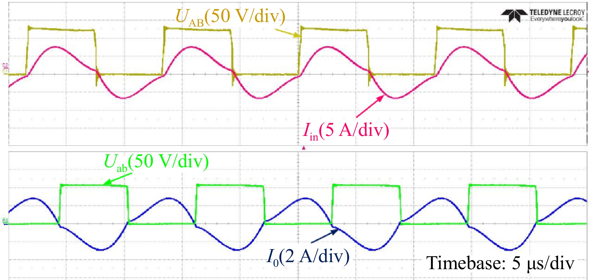
Figure 15.
Experimental waveforms of UAB, Uab, Iin, and Io in the CC mode.
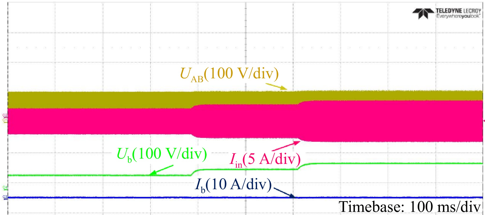
Figure 16.
Experimental waveforms of Ub and Ib in the CC mode with RL varying from 24 to 32 Ω.
Figure 17 shows the experimental waveform of the input/output voltage and current for a resonant network under the CV condition. The inverter includes a ZPA condition, which agrees well with the theoretical analysis. The DC output characteristics under load variation are presented in Fig. 18. It indicates that when the DC resistance increases from 36 to 50 Ω, the DC output power decreases from 178 to 128 W, the output current decrease from 2.25 to 1.6 A, the output voltage remains constant to 80 V. The maximum fluctuation of the system's output current is 2%. In addition, due to the small load resistance value and the single capacitor structure on the secondary side, the AC output current distortion in CV charging mode is smaller than CC charging mode.
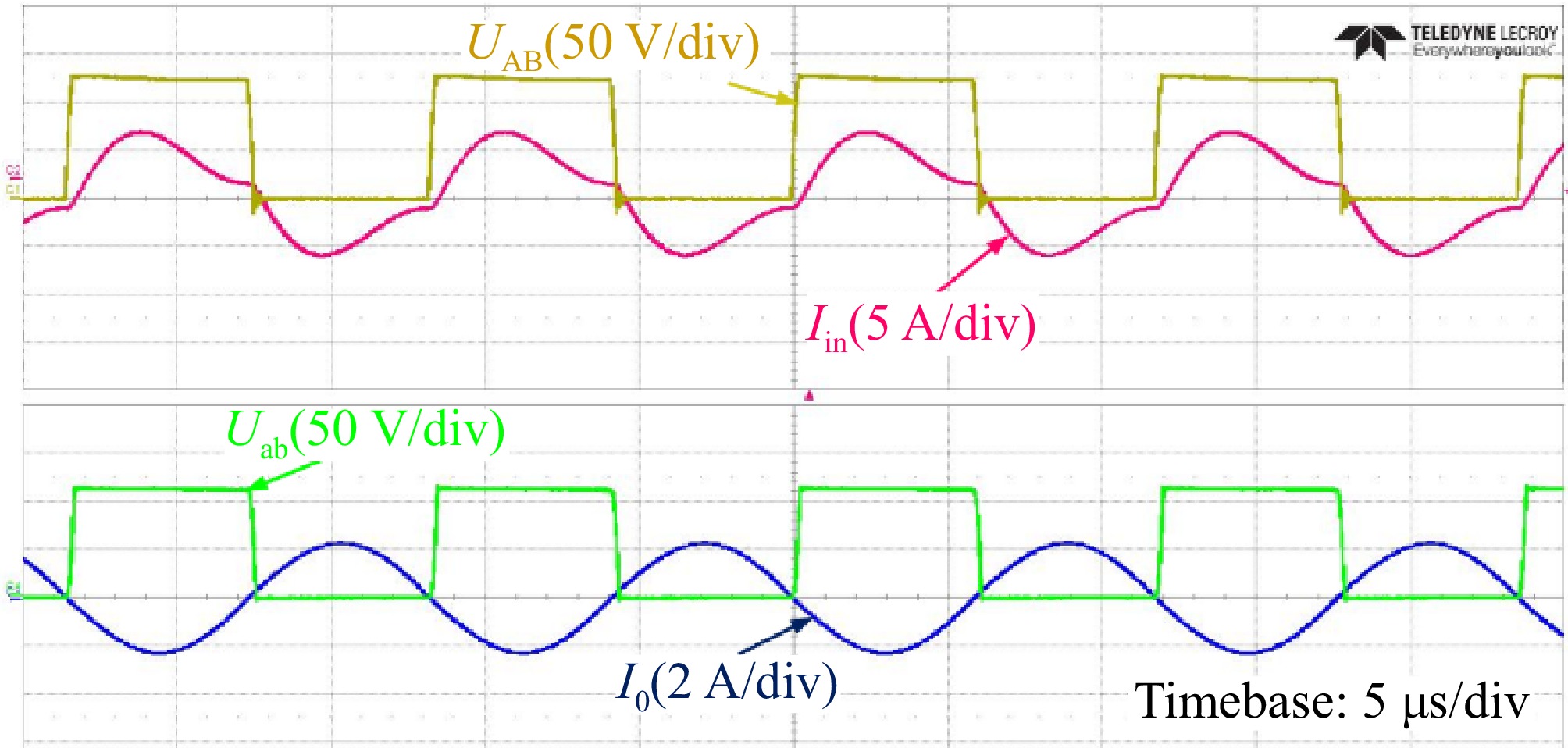
Figure 17.
Experimental waveforms of UAB, Uab, Iin, and Io in the CV mode.
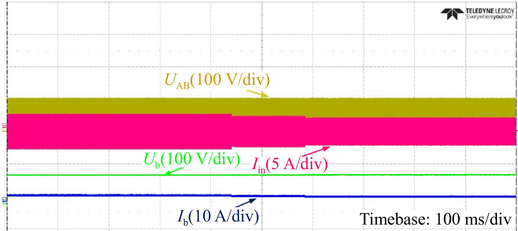
Figure 18.
Experimental waveforms of Ub and Ib in the CV mode with RL varying from 36 to 50 Ω.
Performance of the proposed IPT Charger under the misalignment conditions
-
Figure 19 shows the input voltage and current waveform of the resonant network and rectifier under the well-aligned and 100 mm misalignment conditions for CC charging process. The findings indicate that the inverter achieves ZVS functionality alongside stable operation of the system. In addition, it can be concluded through experiments that the fluctuation range of the output current under the misalignment state is [−2.3%, 3.2%]. This fluctuation range ensures the stability of the system's current during the actual charging process.
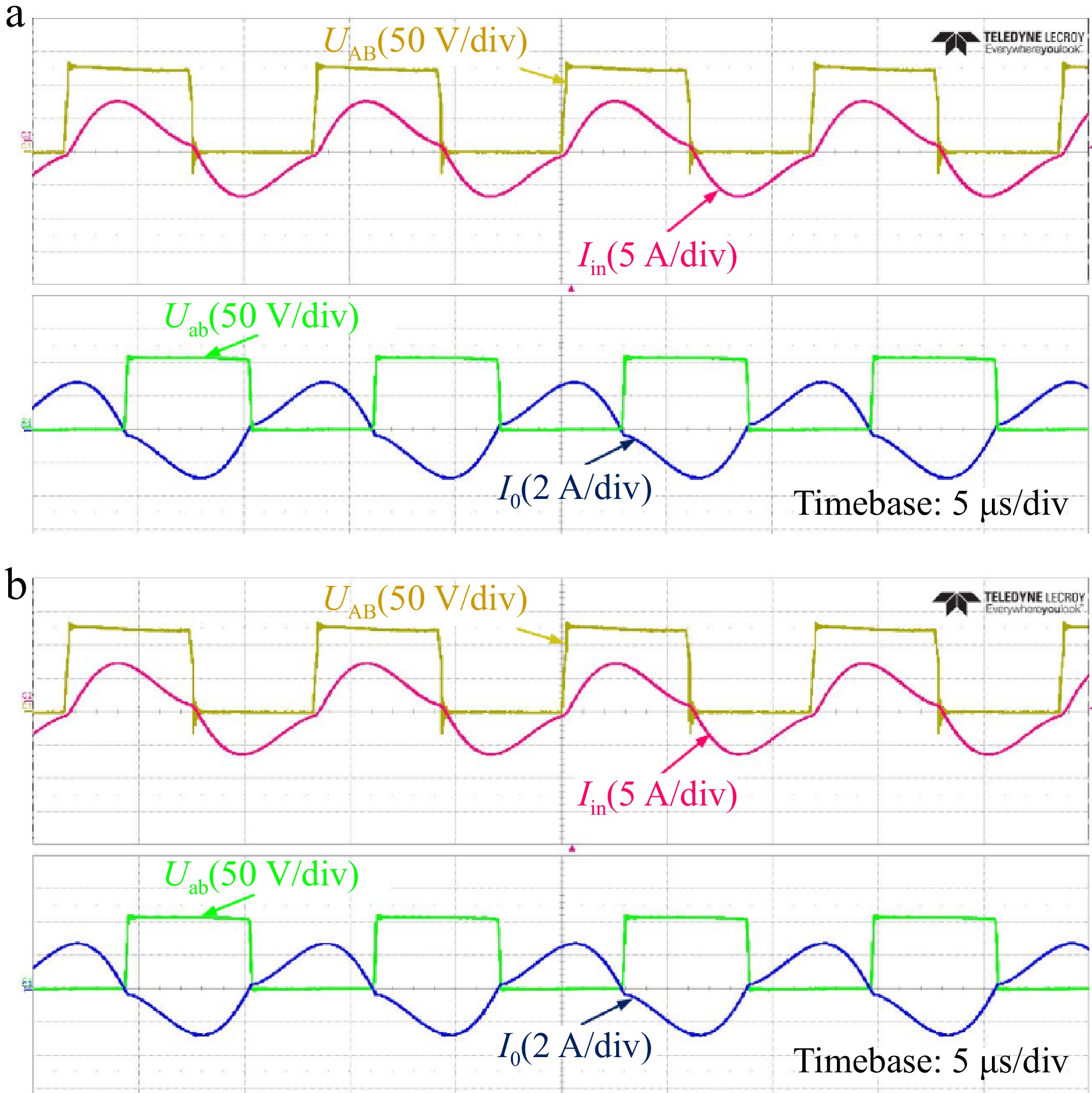
Figure 19.
Experimental waveforms of alignment and misalignment condition in CC mode. (a) Alignment condition. (b) Misalignment condition.
Figure 20 shows the input voltage and current waveform of the resonant network and rectifier under the well-aligned and 100 mm misalignment conditions for CV charging process. Findings indicate that the inverter switches are capable of attaining ZVS, and the system maintains consistent functionality. In addition, it can be concluded through experiments that the fluctuation range of the output voltage under the misalignment state is [−2.5%, 3.7%]. This fluctuation range ensures the stability of the system current during the actual charging process.
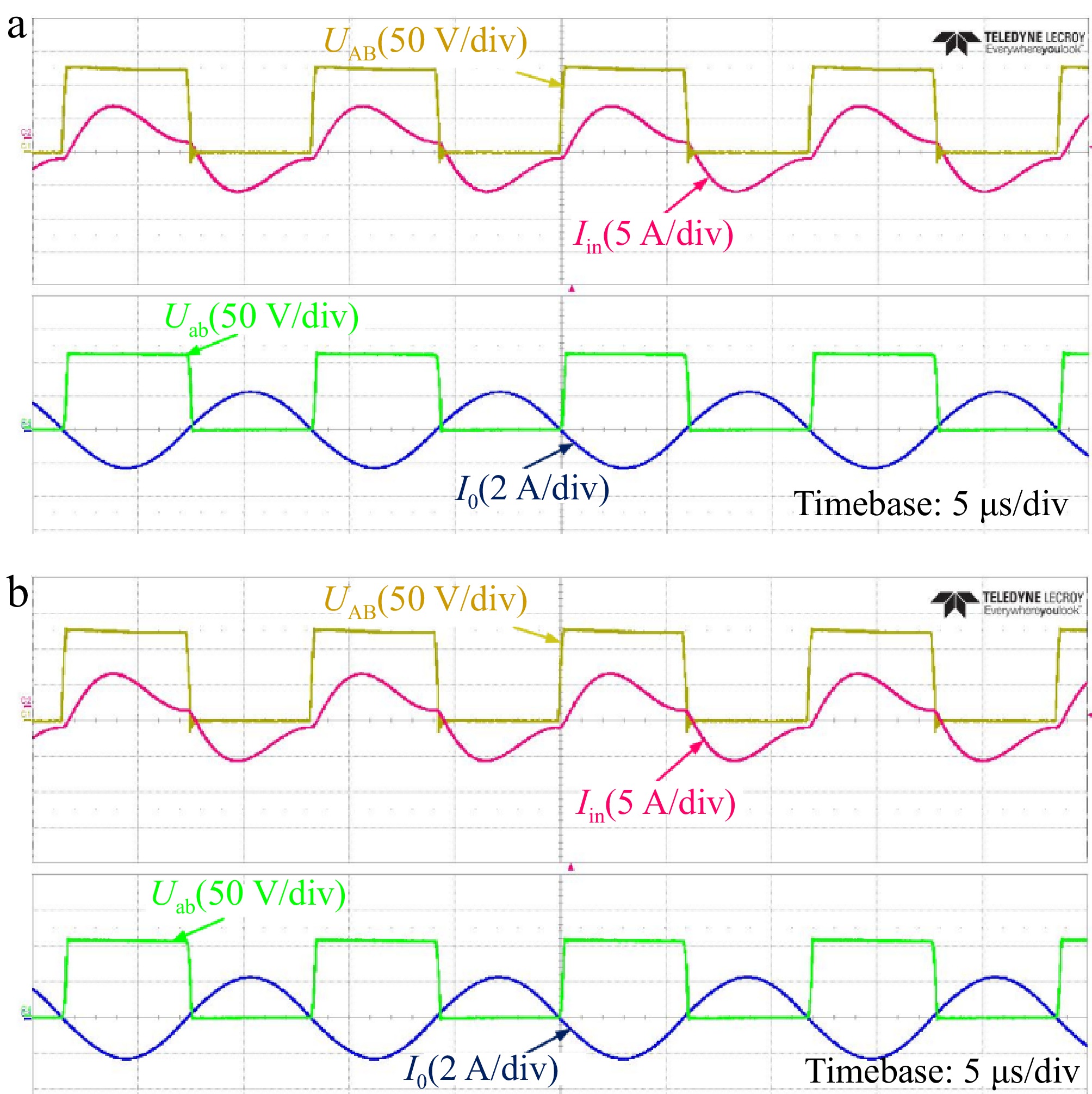
Figure 20.
Experimental waveforms of alignment and misalignment conditions in CV mode. (a) Alignment condition. (b) Misalignment condition.
A comparison with other methods proposed in the literature is shown in Table 4. A high-reliability three-coil hybrid IPT (Inductive Power Transfer) topology is proposed, which exhibits improved tolerance to coupling variation and provides a load-independent output[24]. This paper has several identified weaknesses: the air gap is relatively small, causing a low coupling coefficient; and to initiate CC and CV charging, an extra AC switch is necessary, leading to a rise in the system's overall volume and complexity. Primarily, the proposed technique offers an improved balance between the number of components and the features of the output.
Table 4. Comparison with other methods reported in the literature.
Inductor/
capacitor countsSwitch counts Coils of LCT Misalignment tolerance
X-directionMisalignment tolerance Y-direction Output characteristic Efficiency Max. power Ref. 2/6 4 4 37% 37% CP 85.5%−93.1% 700 W [23] 1/3 4 3 50% 50% CC/CV 88.2%−92.5% 460 W [24] 1/3 4 3 50% 50% CC 76%−84% 200 W [25] 4/6 6 4 50% 12.5% CC/CV 85.7%−93.9% 1 kW [26] 2/6 4 4 37.5% 37.5% CV 87%−93.9% 3.5 kW [27] 1/3 4 2 50% 50% CV 81%−88% 700 W [28] 2/4 4 3 40% 40% CC 92% 3.4 kW [29] 2/4 4 3 50% 50% CC 80.6% 100 W [30] 2/4 4 + 3 3 42% 42% CC/CV 86.5%−92.9% 200 W This work A hybrid and reconfigurable system is introduced to achieve high misalignment tolerance while enabling both CC and CV charging capabilities[25]. The system can operate with misalignment to 50% in the x/y direction, with resistance varying from 36 to 480 Ω, and the output fluctuation remains within 5%. However, the coupling relationship of this coil is relatively complex, and the constant output topology utilizes many active components, increasing system volume and losses. Another article introduces an anti-misalignment WPT system based on an LCC-S topology, featuring dual coupled transmitting coils with reverse-parallel windings[26]. The output remains stable under the misalignment condition. However, this system can only achieve CV charging, and the efficiency is low throughout the charging process. Another approach is to significantly enhance tolerance to horizontal misalignment by introducing an anti-series three-coil LCT configuration[27]. Nevertheless, the design encountered several challenges: the AC resistance of the receiving coil was notably increased due to the numerous turns needed to enhance the self-inductance of LP; adjustments to the air gap D necessitated modifications in coil turns, adding design complexity of the LCT; and the significant misalignment deviation led to fluctuations in the self-inductance of LP.
In response to the challenges faced by the third coil structure, the LCT designed in this paper uses Litz wire with a higher number of strands to reduce the equivalent series AC resistance of the coil. If the application scenario of the wireless charging system has a tolerance on the air gap D, it can be solved using a control strategy, such as using a buck-boost converter on the primary or secondary side, and applying phase shift control or duty cycle control for the inverter. The dimensions of the third coil structure (LP : LS : LT) are set to 240:250:160 mm, optimizing the misalignment tolerance of the LCT in the horizontal direction. In addition, third coils are introduced on the secondary side to alleviate the impact of self-inductance changes on the current/voltage gain and input phase angle of the system.
Figure 21 depicts the output power and system efficiency according to load variations. The maximum system efficiency of CC and CV charging are 92.23% and 92.27% respectively. The maximum efficiency is 92.27% which appears at 123 W for the proposed IPT system.
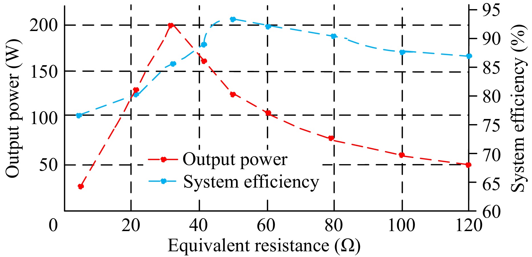
Figure 21.
Efficiency and output power of the proposed IPT system.
Figure 22 illustrates each component's losses and efficiency distribution of the presented system. Losses in the system can be quantified using a power analyzer, and the detailed distribution of losses for each component can be inferred through computational techniques. A power analyzer measures the overall losses and current/voltage amplitudes, followed by a comprehensive calculation of the loss distribution based on the measured currents and voltages[28]. Furthermore, to enhance the accuracy of the loss distribution, core losses were simulated using finite element method simulations[29,30]. Due to the ZVS operation of the power switching device, inverter losses account for a relatively small proportion of the total. The test outcomes reveal that the majority of system losses originate from the coupler.
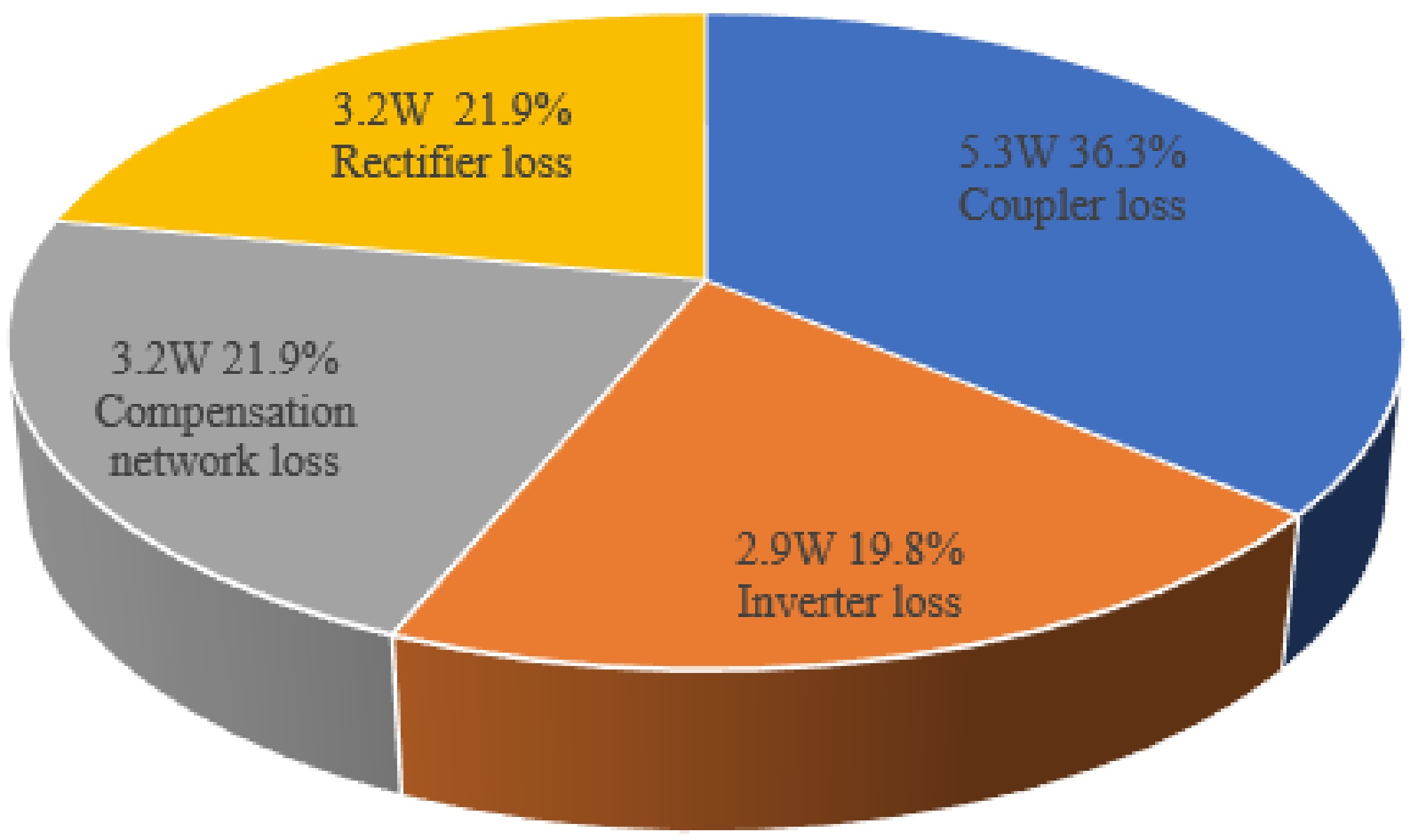
Figure 22.
Efficiency distribution of the proposed IPT system.
Figure 23 illustrates the waveforms captured by the power analyzer under constant voltage (CV) mode, demonstrating a system efficiency of 92.27%. Analysis of the efficiency reveals that the suggested network structure significantly enhances the system's effectiveness.
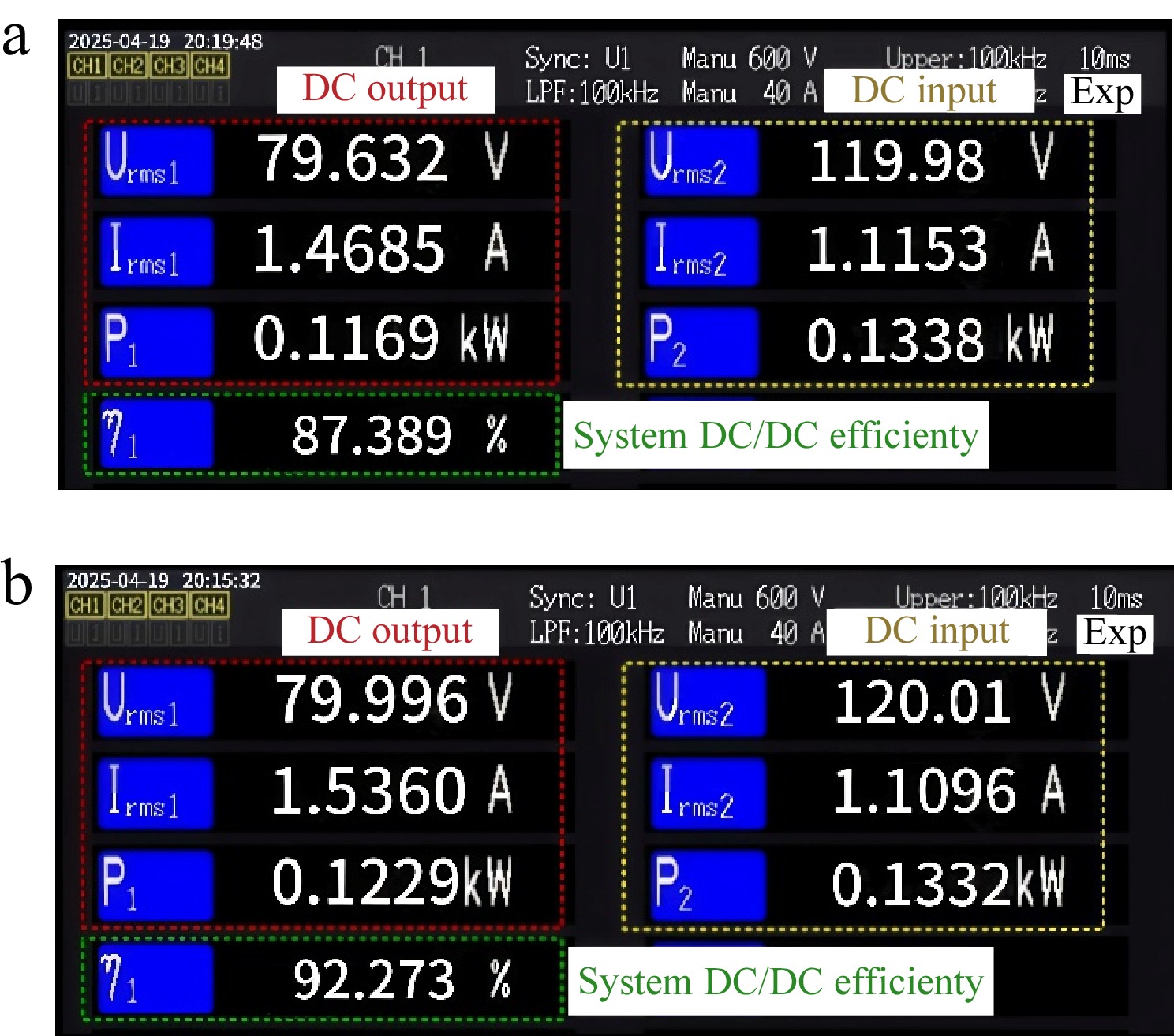
Figure 23.
Power analyzer data in the CV mode. (a) Misaligned state. (b) Aligned state.
Figure 24 illustrates the performance comparison between the proposed three-coil magnetic coupler and the traditional two-coil configuration under misalignment conditions. The results indicate a substantial decline in both output power and system efficiency for the two-coil structure when misaligned. The analysis confirms that the three-coil design offers improved practicality and effectiveness.
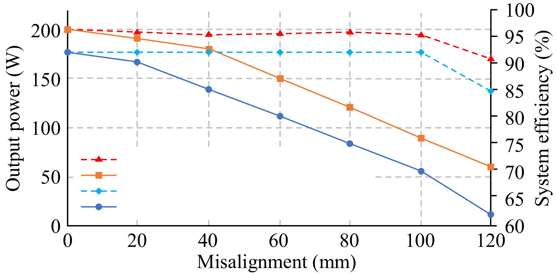
Figure 24.
Output power and efficiency comparison between third-coil and two-coil coupler with misalignment.
-
This paper presents a high-performance wireless charging topology structure that incorporates a third-coil loosely coupled transformer to improve the system's misalignment performance, and utilizes a reconfigurable topology structure to achieve constant current and voltage output. The maximum deviation of the coil in the x and y directions can reach 42%, and the maximum transmission efficiency is 92.27%. This structure does not require communication between the main and ancillary sides and utilizes fewer active components to achieve a higher power density.
This work was supported in part by the Natural Science Foundation of Shangdong Province (Grant No. ZR2022ME214).
-
The authors confirm their contribution to the paper as follows: Study conception and design: Zhang H, Zhou X; data collection: Zhang H, Tian S; analysis and interpretation of results: Zhang H, Tian S, Wang H; draft manuscript preparation: Zhang, Tian S, Wang H, Zhou X. All authors reviewed the results and approved the final version of the manuscript.
-
The data generated or analyzed during the current study are included in this published article and are available from the corresponding author upon reasonable request.
-
The authors declare that they have no conflict of interest.
- Copyright: © 2025 by the author(s). Published by Maximum Academic Press, Fayetteville, GA. This article is an open access article distributed under Creative Commons Attribution License (CC BY 4.0), visit https://creativecommons.org/licenses/by/4.0/.
-
About this article
Cite this article
Zhang H, Tian S, Wang H, Zhou X. 2025. Improving misalignment tolerance for a third coil IPT charger with load-independent output. Wireless Power Transfer 12: e019 doi: 10.48130/wpt-0025-0013 

Improving misalignment tolerance for a third coil IPT charger with load-independent output
- Received: 23 December 2024
- Revised: 21 April 2025
- Accepted: 28 April 2025
- Published online: 07 July 2025
Abstract: This paper proposes a system to improve misalignment tolerance and achieve constant current (CC) and constant voltage (CV) outputs for an electric bicycle inductive power transfer (IPT) charger. Existing systems typically sacrifice output stability when enhancing misalignment tolerance and often rely on complex control circuits for CC-CV switching. A tertiary coil is utilized to establish a reverse connection with the secondary side coil without affecting the inherent output characteristics. The loosely coupled transformer with a third coil can effectively improve the misalignment tolerance in the x- and y-directions. In addition, a simple and reconfigurable structure is developed, enabling shifts from inductor-capacitor-capacitor-inductor-capacitor-capacitor (LCC-LCC) topology to inductor-capacitor-capacitor-series (LCC-S) topology, and further acquiring load-independent CC and CV outputs. The proposed tri-coil design simultaneously addresses misalignment challenges while eliminating control complexity. JMAG simulation and experimental findings confirm the accuracy of the suggested model and its structural design. The experimental results show that the prototype achieves an output power of 200 W with a maximum efficiency of 92.7%.
-
Key words:
- High-misalignment tolerance /
- Hybrid IPT systems /
- CC charging /
- CV charging