


-
With the rapid development of technology and increasing attention to efficient energy utilization and environmental protection, wireless power transfer has become an important research direction in the field of energy transmission due to its high efficiency, convenience, and eco-friendly characteristics[1−4]. Among various wireless power transfer technologies, microwave wireless power transfer has emerged as a novel approach that uses high-frequency microwave signals to transfer electric power through space. It not only overcomes the dependence on physical contact in traditional transmission methods but also achieves long-distance energy transfer[5]. This technology demonstrates excellent flexibility in dynamically changing environments and supports point-to-point rapid energy transfer with minimal environmental influence, thereby significantly enhancing the adaptability and reliability of transmission systems[6]. Applications range from low-power sensors and remote controllers to unmanned aerial vehicles (UAV) and electric vehicles that require long-distance range extension, and even solar power stations in space[7,8]. The structure of a microwave wireless power transfer system is shown in Fig. 1.
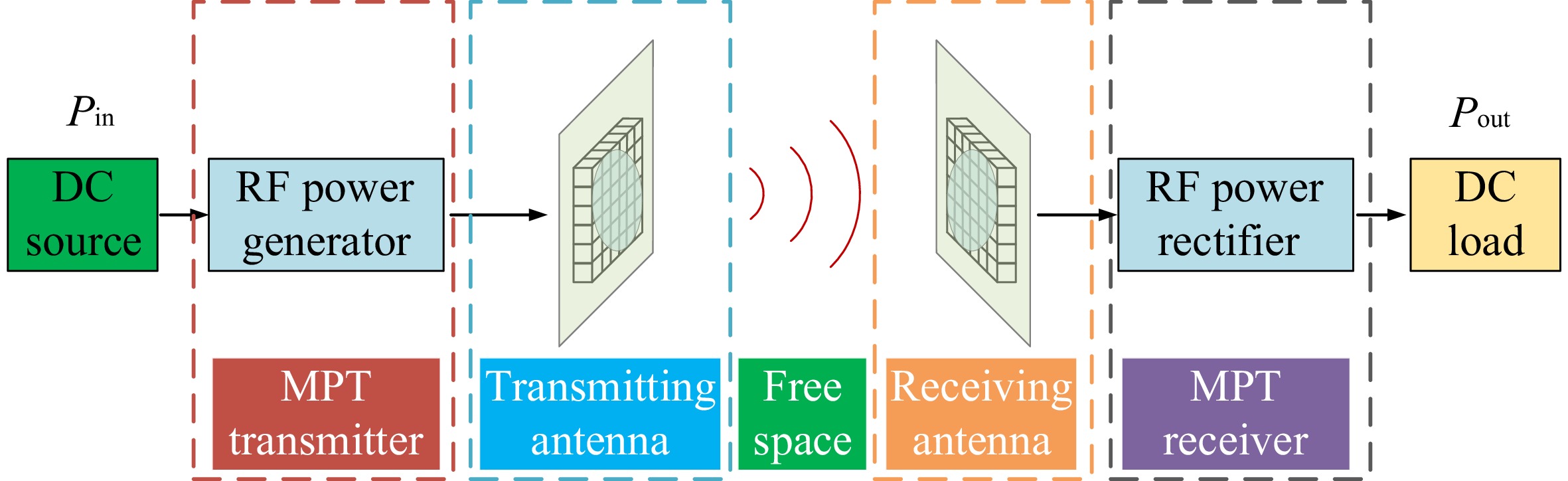
Figure 1.
The structure of a microwave wireless power transfer system.
Along with the continuous popularization of the Internet of Things and the gradual establishment of the Energy Internet, there is an increasing need for efficient energy scheduling and real-time interaction. In practical applications, energy transfer demands are often not limited to a unidirectional source-to-load mode. When a UAV makes a short landing at a ground station or in a mother-ship formation, it needs to complete high-speed bidirectional energy exchange within a limited time[9]. Under the Vehicle-to-Grid architecture, electric vehicles can wirelessly feed excess energy back to the power grid to balance the peak-valley difference and improve the overall energy utilization efficiency[10]. If a unidirectional transfer or discrete transceiver design is adopted, the system size and cost increase and the flexible management of bidirectional power flow becomes difficult. Therefore, bidirectional energy transfer technology can flexibly switch between charging and discharging functions among different carriers, not only balancing the dynamic changes in energy production and consumption but also achieving more efficient energy distribution and load scheduling, significantly improving overall system reliability and adaptability. This makes bidirectional circuit design a key technical aspect for energy interconnection and intelligent management.
Power amplifiers and rectifiers are the core modules of microwave wireless power transfer systems[11−13], but many challenges remain when implementing bidirectional energy transfer. Traditional radio-frequency power amplifiers have been designed based on transistor technologies. For instance, Sharma et al. designed an inverse Class-F power amplifier with an output power of 40 dBm, a drain efficiency of 76%, and a gain of 12 dB[14]. Rectifiers for low-power scenarios usually utilize diodes. For example, He et al. developed a broadband Schottky diode rectifier with an efficiency of over 70% in the range 1.6–2.8 GHz[15]. Zhang et al. used a diode array to increase the power capacity, achieving a peak efficiency of 69.4% at 2.45 GHz when the output power reached 30 dBm[16]. Liou et al. adopted a strategy combining RF power division and DC power synthesis to increase rectifier power capacity[17]. However, the complex distribution network introduces additional losses that reduce efficiency. Thus, when attempting to increase the rectification power capacity, conventional methods typically face reduced energy conversion efficiency.
Recently, GaN high electron mobility transistor (HEMT) rectifiers have become a research focus. Haider et al. designed a self-synchronous rectifier with a phase-shifting network that achieved a peak rectification efficiency of 84.94% at 2.85 GHz, delivering 8.49 W of DC output power[18]. However, when such circuits are used in bidirectional designs, the feedback phase-shifting network may cause self-oscillation in the power amplifier, compromising the system stability and reliability. In summary, although bidirectional microwave wireless power transfer has significant theoretical and practical potential, it also faces major technical bottlenecks such as high-power rectification, feedback network stability, and multi-module collaborative integration. Current research on this technology is still relatively limited, and the realization of bidirectional functionality will create new opportunities and challenges for microwave wireless power transfer.
In response to the above research context, this paper proposes a bidirectional microwave wireless power transfer system. The key innovations are as follows:
1. A highly integrated bidirectional wireless power module is proposed, enabling flexible switching between the power amplifier (PA) and rectifier modes to satisfy bidirectional energy transfer requirements on the same hardware platform.
2. The conventional feedback phase-shift network in the GaN HEMT rectifier structure is removed, and the system layout is compactly designed to eliminate the risk of self-oscillation at high power levels in the bidirectional system.
3. System-level collaborative verification is performed to demonstrate the feasibility of bidirectional transfer in real-world scenarios.
-
Figure 2 illustrates the structure of the bidirectional microwave wireless power transfer system. Through a switch in the system, the bidirectional power module can freely switch between the PA and rectifier modes, thereby achieving DC-RF and RF-DC energy conversions in two directions.
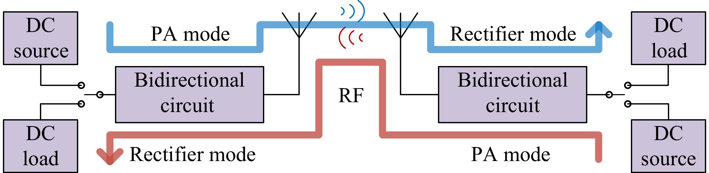
Figure 2.
Structure of the bidirectional microwave wireless power transfer system. Blue lines represent forward power flow, red lines represent reverse power flow.
As the core power conversion core of a microwave wireless power transfer system, power amplifiers, and rectifiers are key modules for bidirectional energy transfer design. According to the time-reversal duality proposed Hamill[19], a high-efficiency rectifier circuit can be realized by a power amplifier. Figure 3a and b show the typical circuit structures of a power amplifier and a rectifier, respectively. The power amplifier consists of an input-matching network, a harmonic control network, and an output-matching network. Under normal operation, DC power is delivered from the DC side to the RF load side, achieving DC-RF energy conversion. In rectification mode, the power flow is reversed. The RF signal is fed from the PA's RF output port, and DC power is extracted from the drain side, achieving RF-DC energy conversion.
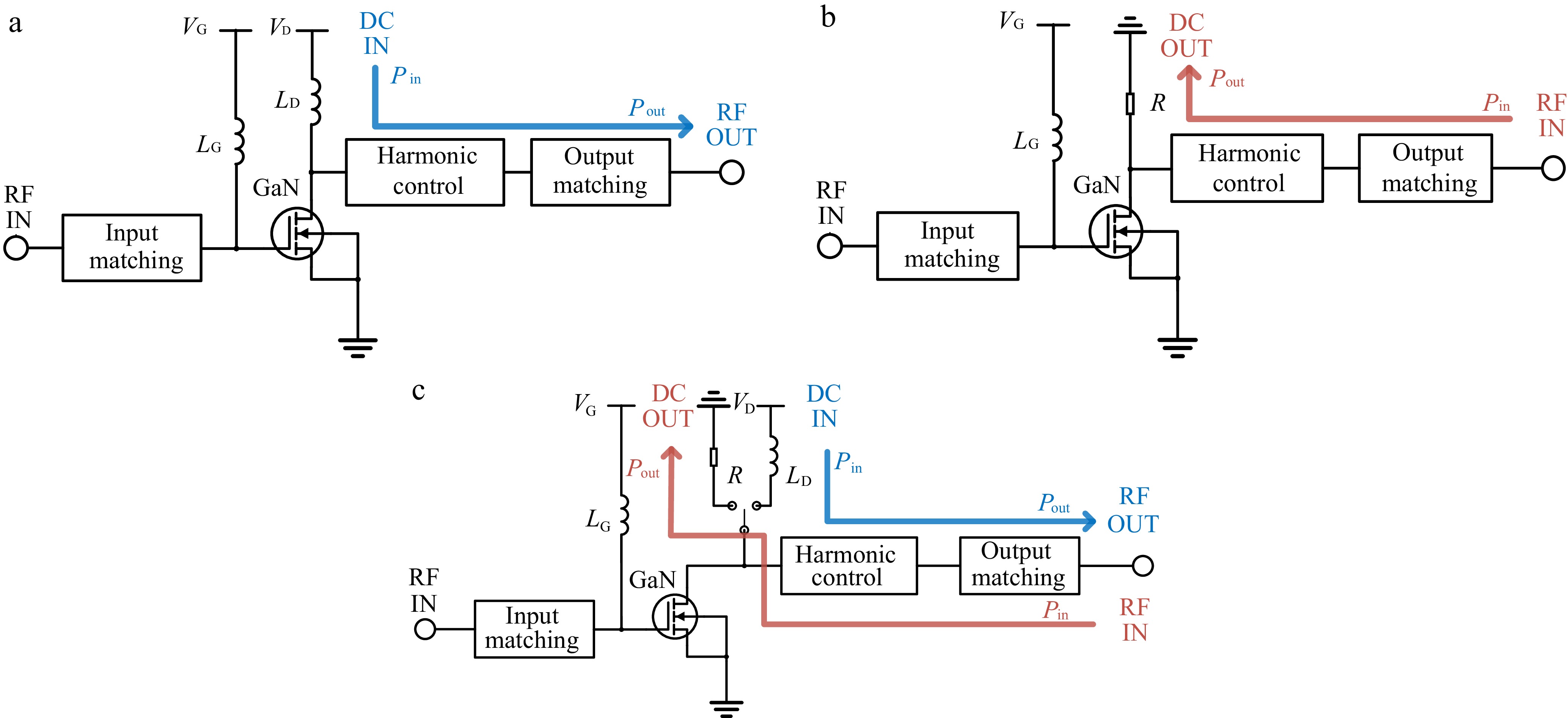
Figure 3.
System diagrams. (a) Power amplifier, (b) rectifier, (c) bidirectional circuit.
The bidirectional system proposed in this paper is shown in Fig. 3c. By combining the circuit characteristics of the power amplifier and the rectifier, and utilizing switching circuitry on the drain side to toggle between the DC power supply and the DC load, flexible mode switching is achieved. When the drain side is connected to a DC power source, the system operates in PA mode, and the control signal fed to the gate drives the transistor into forward conduction, thereby completing forward power delivery. When the drain side is connected to a DC load, the system operates in Rec mode, and the gate control signal is reversed such that the transistor is in reverse conduction, realizing reverse power delivery. This bidirectional system design combines the functionalities of amplification and rectification, which not only reduces the system complexity and design cost but also enables integrated design for the practical implementation of microwave bidirectional wireless power transfer.
When the power amplifier is used for rectification, the relationships between the drain voltage and current for the power amplifier and rectifier are expressed as follows:
$ v_{\text{d,Rec}}\left(t\right)=v_{\text{d,PA}}\left(-t\right) $ (1) $ i_{\text{d,Rec}}\left(t\right)=-i_{\text{d,PA}}\left(-t\right) $ (2) where, vd,Rec and vd,PA are the transistor drain voltages in the rectifier and PA circuits, respectively; id,Rec and id,PA are the transistor drain currents in the rectifier and PA circuits, respectively. Taking the inverse Class-F circuit as an example, the ideal drain voltage and current can be written as:
$ v_{\text{d}}\left(t\right)=v_0+v_1\sin\left(\omega t\right)+v_n\sum\limits_{n=2,4,6,...}^{ }\sin(n\omega t) $ (3) $ i_{\text{d}}\left(t\right)=i_0+i_1\sin\left(\omega t\right)+i_n\sum\limits_{n=3,5,7,...}^{ }\sin(n\omega t) $ (4) where, ω is the fundamental angular frequency, and vn and in are the amplitudes of the nth harmonic voltage and current, respectively. By controlling harmonic impedances, odd harmonics are short-circuited and even harmonics are open-circuited, shaping the drain voltage to be a half-sine wave and the drain current to be a square wave, thus minimizing the overlap of voltage and current in the time domain, thereby reducing loss and improving rectification efficiency. According to the time-reversal duality theory, the drain voltage and current waveforms in the PA and rectifier modes are shown in Fig. 4a and b, respectively.
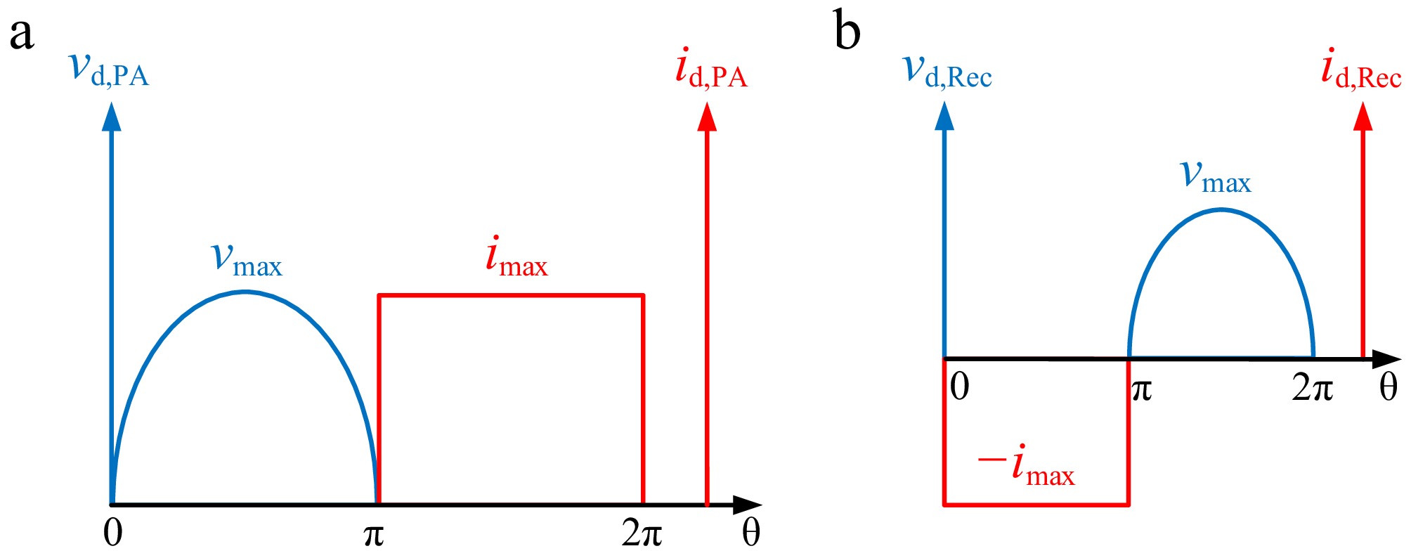
Figure 4.
Ideal drain voltage and current waveforms of (a) PA, and (b) rectifier.
There is a clear structural and energy-transfer symmetry between power amplifiers and rectifiers. The DC supply port and RF output port of the power amplifier can be reversed to serve as the DC output port and RF input port of the rectifier. To transform from a power amplifier into a rectifier, the key lies in reversing the drain current, making the transistor enter reverse conduction. In this paper, the reverse conduction of the GaN HEMT transistor is realized via its intrinsic body diode between the drain and source (as shown in Fig. 5). When the gate bias voltage sets the transistor in the cutoff region, the transistor appears open-circuited at high drain input levels. Meanwhile, when the drain input signal is at a low level, the body diode provides reverse conduction, which is consistent with the state expected by the time-reversal duality theory.
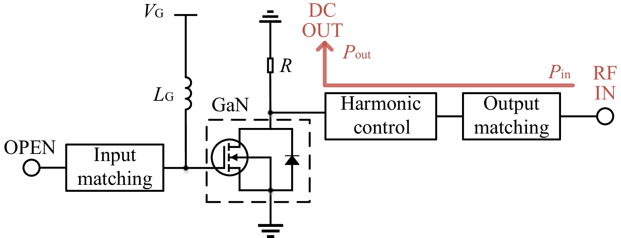
Figure 5.
Compact rectifier mode with the GaN HEMT.
In reverse conduction mode, the GaN HEMT transistor behaves similarly to a diode. Owing to its high breakdown voltage and high-temperature stability, it can achieve high-power microwave rectification compared to traditional Schottky diode rectifiers. Moreover, this approach eliminates the feedback phase-shifting network commonly used in GaN HEMT rectifier structures, reducing the inherent circuit losses and design complexity while shrinking the circuit footprint. These improvements significantly enhance the feasibility of the circuit for practical engineering applications, providing a technical foundation for implementing high-power microwave bidirectional wireless power transfer systems.
In the PA mode, the drain efficiency and power-added efficiency (PAE) are important metrics for evaluating energy conversion efficiency:
$ \eta_{\text{d}}=\dfrac{P_{\text{RF,OUT}}}{P_{\text{DC,IN}}} $ (5) $ {\text{PAE}} = \dfrac{{{P_{{\text{RF,OUT}}}} - {P_{{\text{RF,IN}}}}}}{{{P_{{\text{DC,IN}}}}}} , $ (6) where, PRF,OUT is the RF output power; PRF,IN is the RF input power; and PDC,IN is the DC input power. In rectifier mode, the rectification efficiency is the main metric for energy conversion efficiency:
$ {\eta _{{\text{Rec}}}} = \dfrac{{{P_{{\text{DC,OUT}}}}}}{{{P_{{\text{RF,IN}}}}}} , $ (7) where, PRF,IN is the RF input power and PDC,OUT is the DC output power. These metrics will be used to evaluate the energy conversion efficiency of the system in subsequent tests.
-
The design of the bidirectional transmission system consists of two main parts: (1) the bidirectional system design, and (2) the array antenna design. The details of each part are provided below.
Bidirectional system design
-
To validate the concept of the bidirectional system, a bidirectional integrated system with power amplification and rectification functions is designed. Currently, the primary frequencies used in the microwave wireless power transfer system are 2.45 and 5.8 GHz. This design uses the 2.45 GHz frequency. A CGH40010F GaN transistor from Cree is utilized along with a Rogers 4350b substrate (εr = 3.66, H = 30 mils). The system architecture is shown in Fig. 6.
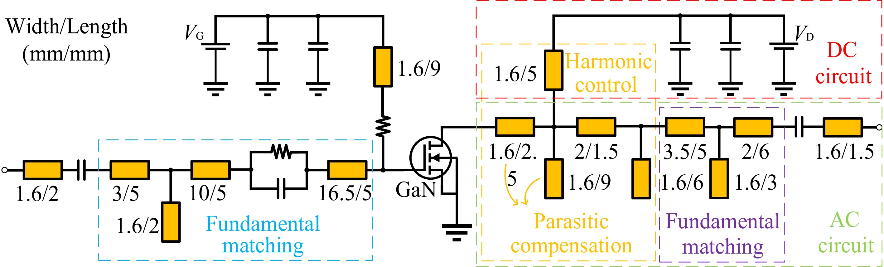
Figure 6.
System architecture diagram with equivalent parameters.
First, an inverse Class-F power amplifier is designed. The design process is collaboratively validated through ADS simulations and primarily consists of an input impedance matching network, a harmonic control network, and an output matching network. The gate voltage is −3.4 V, and the drain voltage is 28 V. Since parasitic parameters of the transistor, including drain-to-source capacitance Cds, parasitic inductance Ld , and the external packaging capacitance Cp. To enhance the overall system performance, an L-type compensation structure is added to the front end of the harmonic control network. This mitigates the negative impact of parasitic parameters and improves energy conversion efficiency.
In designing the harmonic control network, only the second and third harmonics are considered to reduce system complexity and facilitate bidirectional functionality. As shown in Fig. 7a, O denotes an open circuit and S denotes a short circuit. Based on the impedance transformation characteristics of the wavelength transmission line, TL1 has a length of one-sixth wavelength for short-circuiting the third harmonic, while TL2 and TL3 are two sections of one-eighth wavelength for open-circuiting the second harmonic. The ADS simulation results in Fig. 7b show that the network exhibits high impedance (open) at 4.9 GHz and low impedance (short) at 7.35 GHz, meeting the design requirements.
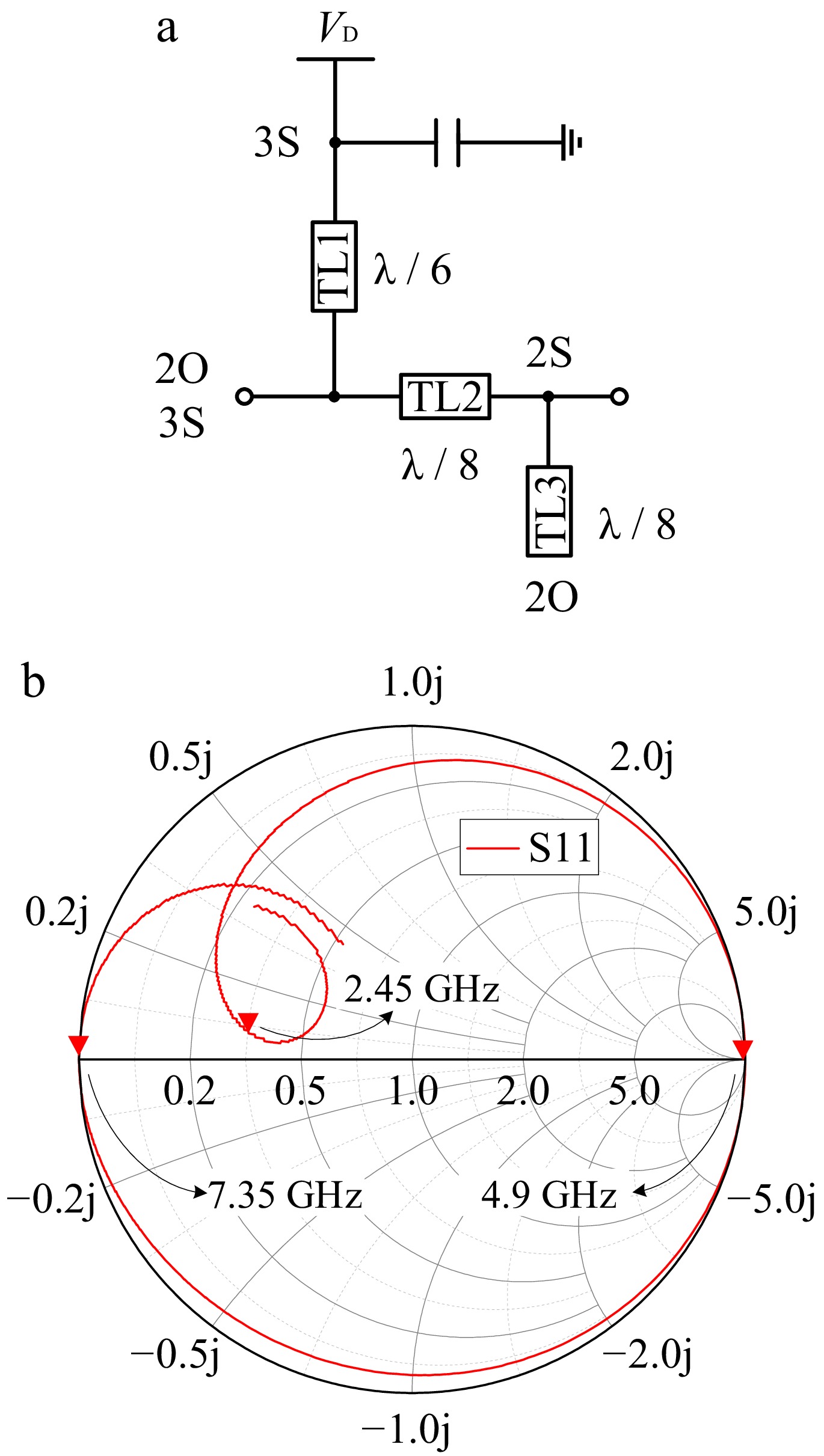
Figure 7.
(a) Schematic of the harmonic network. (b) Calculated results of the input impedance of the harmonic network on on the Smith chart.
Through load-pull and source-pull simulations, the optimal load impedance and optimal source impedance for the power amplifier are found to be (23.2-j15.5) Ω and (3.5-j3.1) Ω, respectively. By applying the Smith chart matching tool, the 50 Ω impedance is transformed to the corresponding optimum impedances, forming the output matching network and input matching network for the fundamental frequency. The Smith chart for the output impedance matching is shown in Fig. 8 (the input impedance matching is designed similarly). In addition, an RC stabilization network is added to the input side to ensure stable long-term operation of the power amplifier near the working frequency.
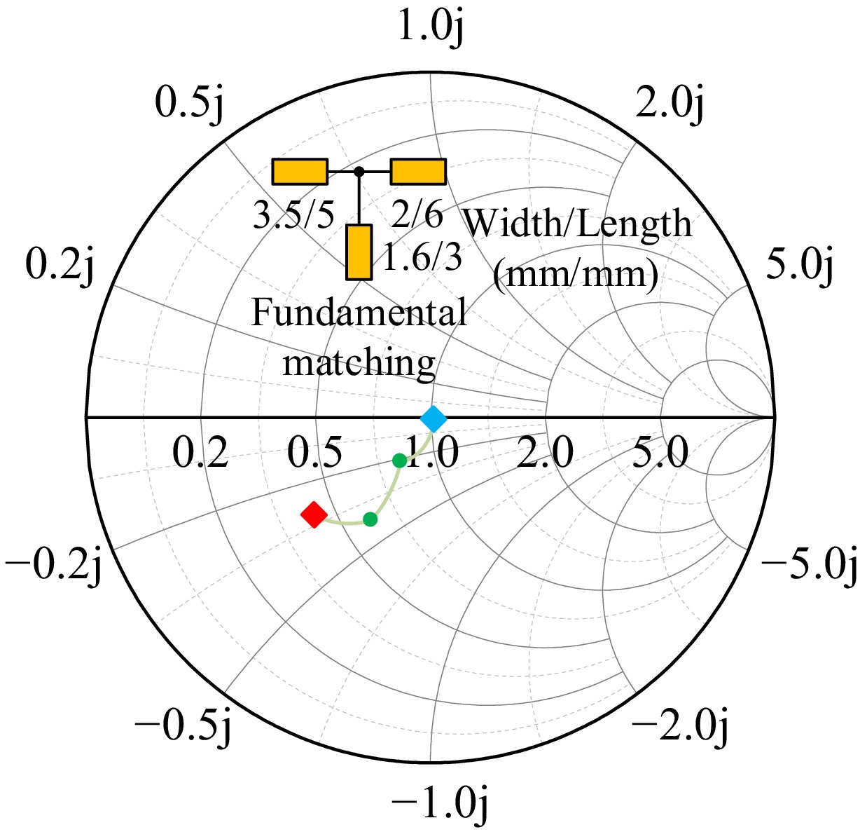
Figure 8.
Smith chart for output impedance matching.
After the design of each module was completed, simulations for the rectifier mode showed that the optimal input impedance of the rectifier is (6.5-j5.0) Ω, which is not significantly different from that in PA mode, meaning the same output matching can be shared. By optimizing the overall system layout, the performances of the power amplifier and rectifier modes are balanced. The final system size is shown in Fig. 6. In the PA mode, the system output power reaches 41.5 dBm with a drain efficiency of 79.19%. In the rectifier mode, the power conversion efficiency is even higher, achieving a rectification efficiency of 85.5%.
Microstrip array antenna design
-
To verify the feasibility and overall performance of the bidirectional system and to ensure the integrity of the microwave wireless power transfer system, this paper designs a set of microstrip array antennas operating at 2.45 GHz. Compared with single-element antennas, array antennas can achieve higher gain and longer transmission distances, meeting the requirements for high-power microwave energy transfer. As shown in Fig. 9, the size of a single antenna unit is 268 mm × 268 mm. The substrate is 2 mm-thick polytetrafluoroethylene (εr = 2.65, tanδ = 0.001). Each unit contains a 4 × 4 array of square patch radiators connected by an evenly distributed microstrip power division network, forming a compact, high-gain array structure. The specific parameters of the antenna unit are listed in Table 1.
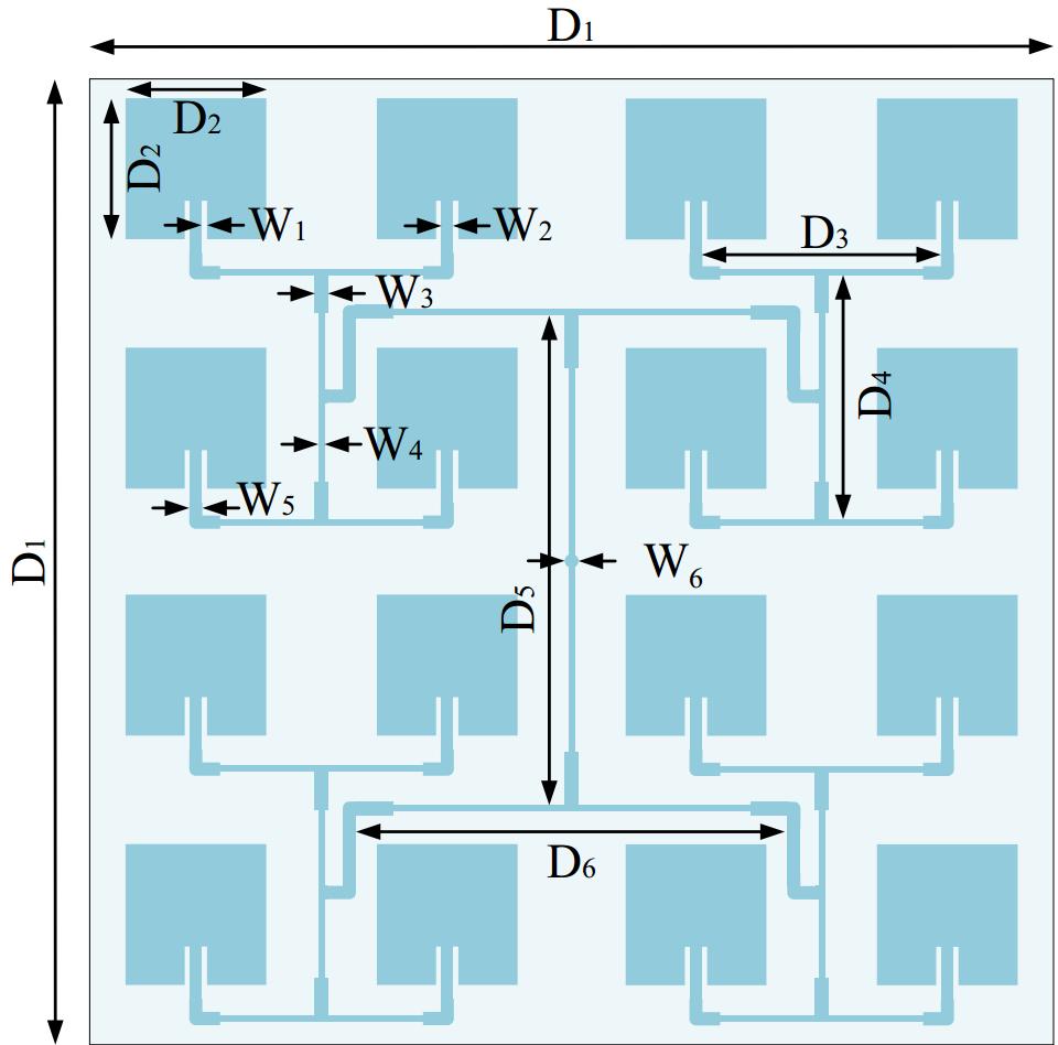
Figure 9.
Structure of the antenna unit.
Table 1. Dimensions of the antenna unit
Variables Unit (mm) Variables Unit (mm) D1 268.0 W1 1.7 D2 37.4 W2 2.5 D3 63.8 W3 3.2 D4 65.5 W4 1.5 D5 131.8 W5 3.2 D6 116.1 W6 4.0 Finite element analysis is conducted using CST electromagnetic simulation software to calculate the performance of the antenna unit. At the operating frequency of 2.45 GHz, the reflection coefficient result is shown in Fig. 10, where S11 is −24.5 dB, meeting the design criteria. The radiation patterns in the E-plane and H-plane are shown in Fig. 11, and the antenna gain reaches 17.6 dBi.
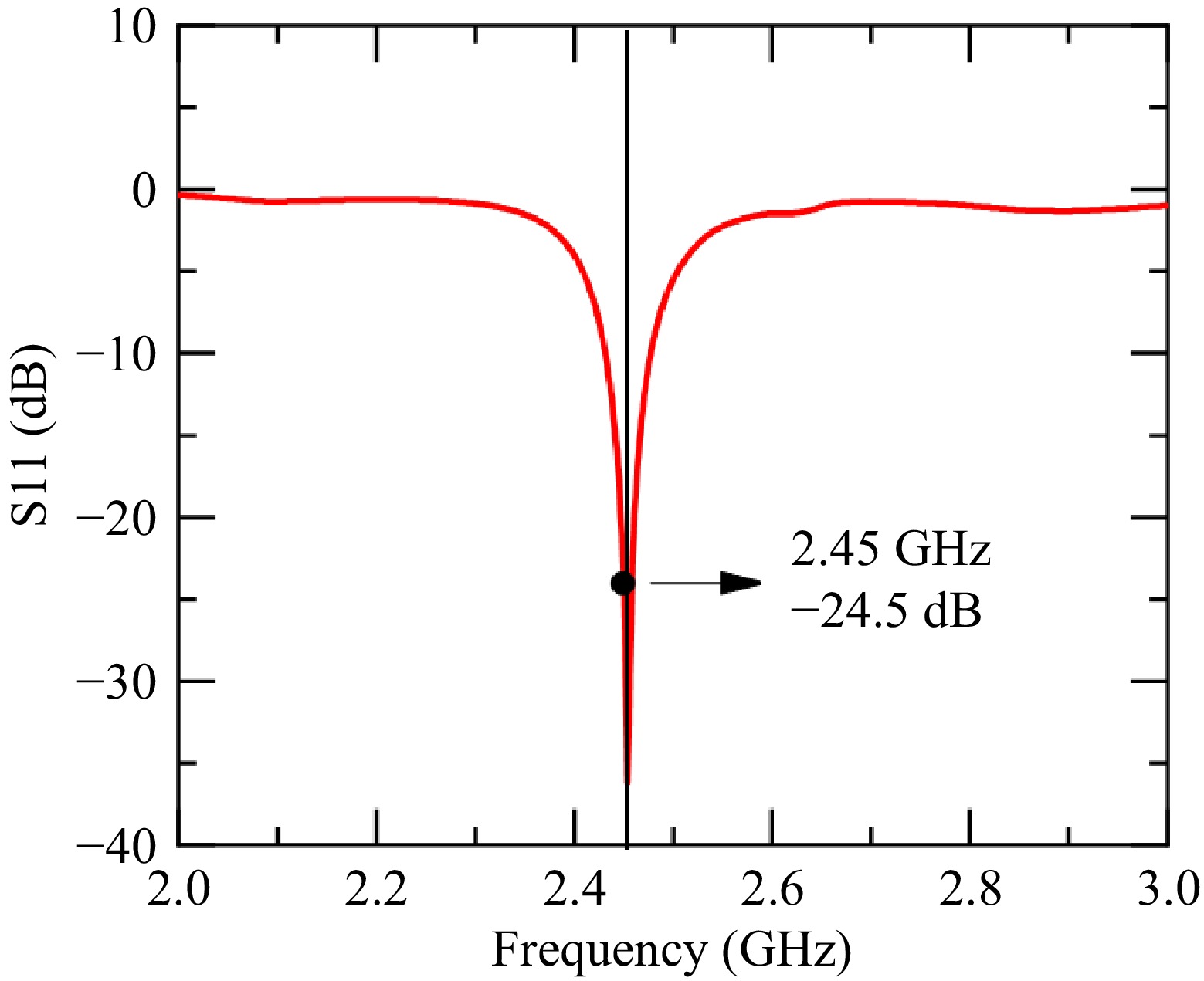
Figure 10.
S11 parameter of the microstrip array antenna.
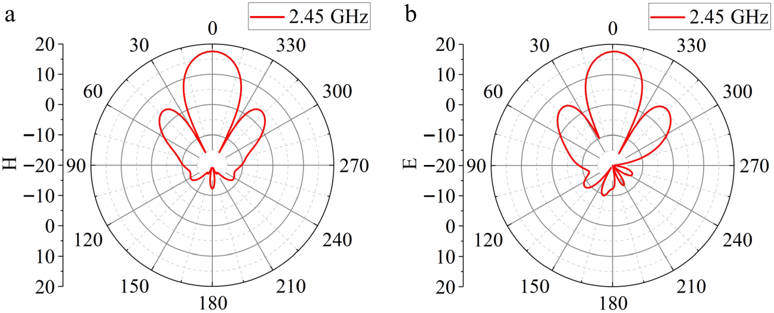
Figure 11.
Radiation patterns of the microstrip array antenna. (a) H-plane, (b) E-plane.
Considering both the transmission performance of the antenna and the project budget, a microstrip array antenna composed of 4 × 4 units is finally selected, giving a total size of 1,080 mm × 1,080 mm. The array antenna feed ports are connected via 16 coaxial cables of equal length to ensure identical phase shifts. These 16 signals are combined into a single port through five 1-to-4 power splitters and then connected to the bidirectional system, forming the antenna feeding network. To evaluate the performance of the bidirectional microwave wireless power transfer system, identical antenna arrays are used on both the transmitting and receiving sides, ensuring that each side can serve as either a transmitter or a receiver. The actual antenna array is shown in the following section.
-
Based on the theoretical analysis and simulation results presented earlier, the bidirectional system and the array antennas were fabricated. Figure 12 shows the actual fabricated items. The experiment includes three parts: testing the performance of the bidirectional system in PA mode; testing the performance of the bidirectional system in rectifier mode; and testing the overall microwave wireless power transfer performance of the system. The test setup for bidirectional system performance is shown in Fig. 13.
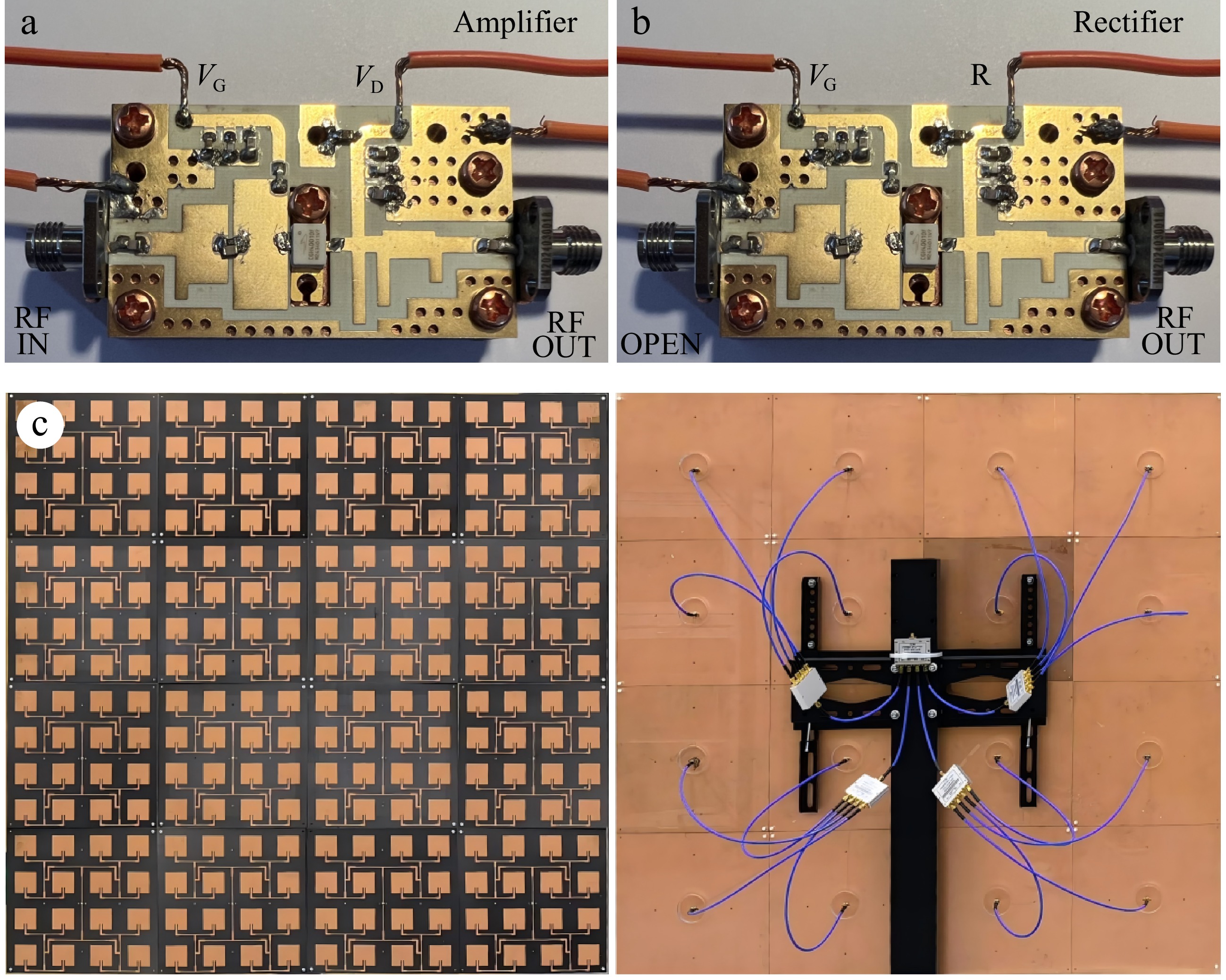
Figure 12.
Fabricated prototypes. (a) PA, (b) rectifier, and (c) microstrip array antenna.
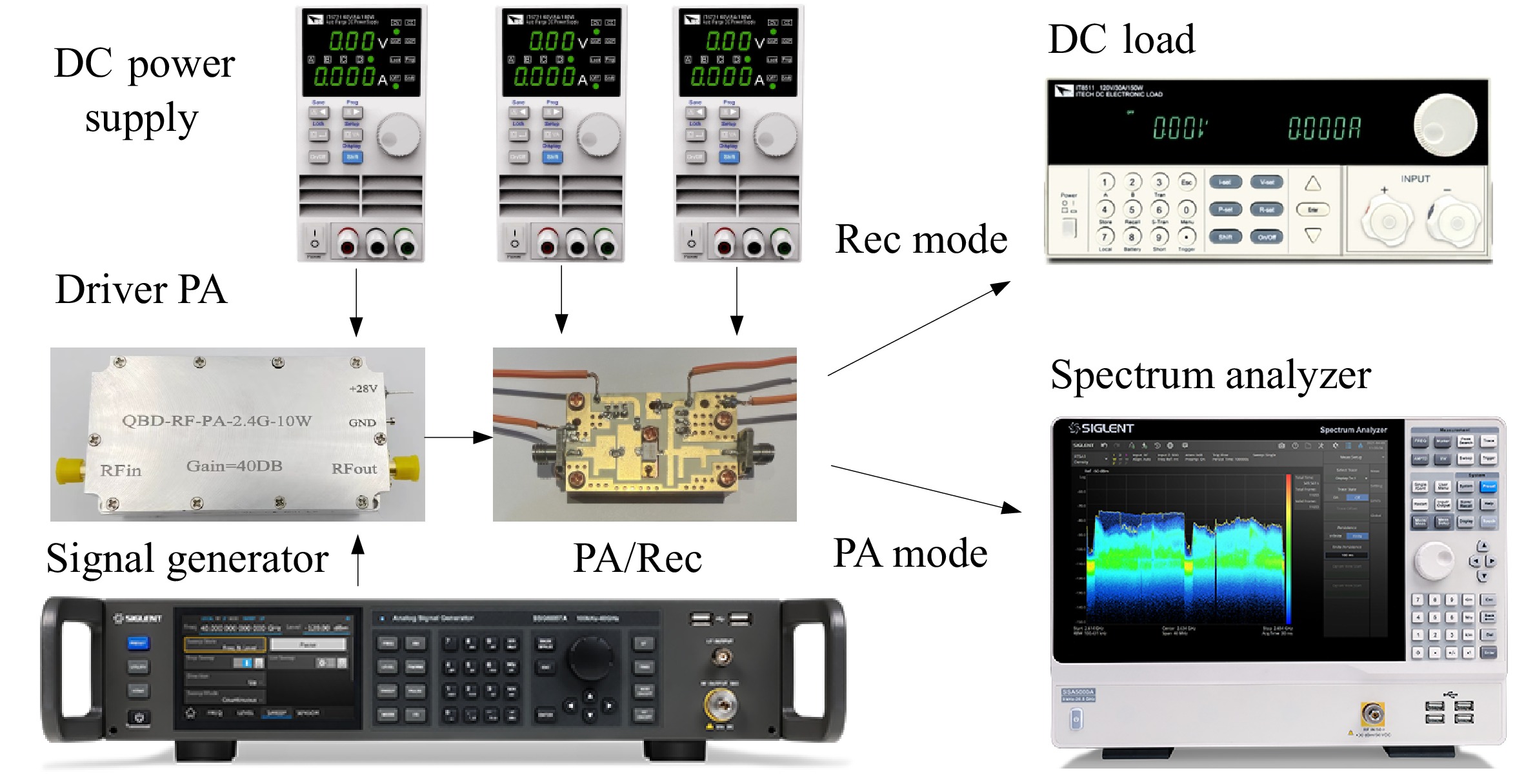
Figure 13.
Experimental setup for evaluating bidirectional system performance.
Power amplifier performance test
-
A test system was built for the PA mode. In the test, the gate voltage was set to −3.4 V and the drain voltage to 27.98 V. The efficiency and gain were measured under different input power levels. The results are shown in Fig. 14. Figure 14a shows the output power and gain curves in the PA mode, with the maximum gain reaching 10.89 dB. Figure 14b presents the drain efficiency and PAE. At an input power of 30 dBm, the output power reaches 40.1 dBm, with a gain of 10.1 dB, DE of 78.68%, and PAE of 70.76%. Compared to the simulation results (maximum output power of 41.5 dBm), the actual measured results are slightly lower due to differences between the transistor's actual parameters and the simulation model, as well as additional losses introduced during soldering. Nevertheless, the overall performance and trend are highly consistent with the simulation, confirming the effectiveness of the bidirectional system in the PA mode.
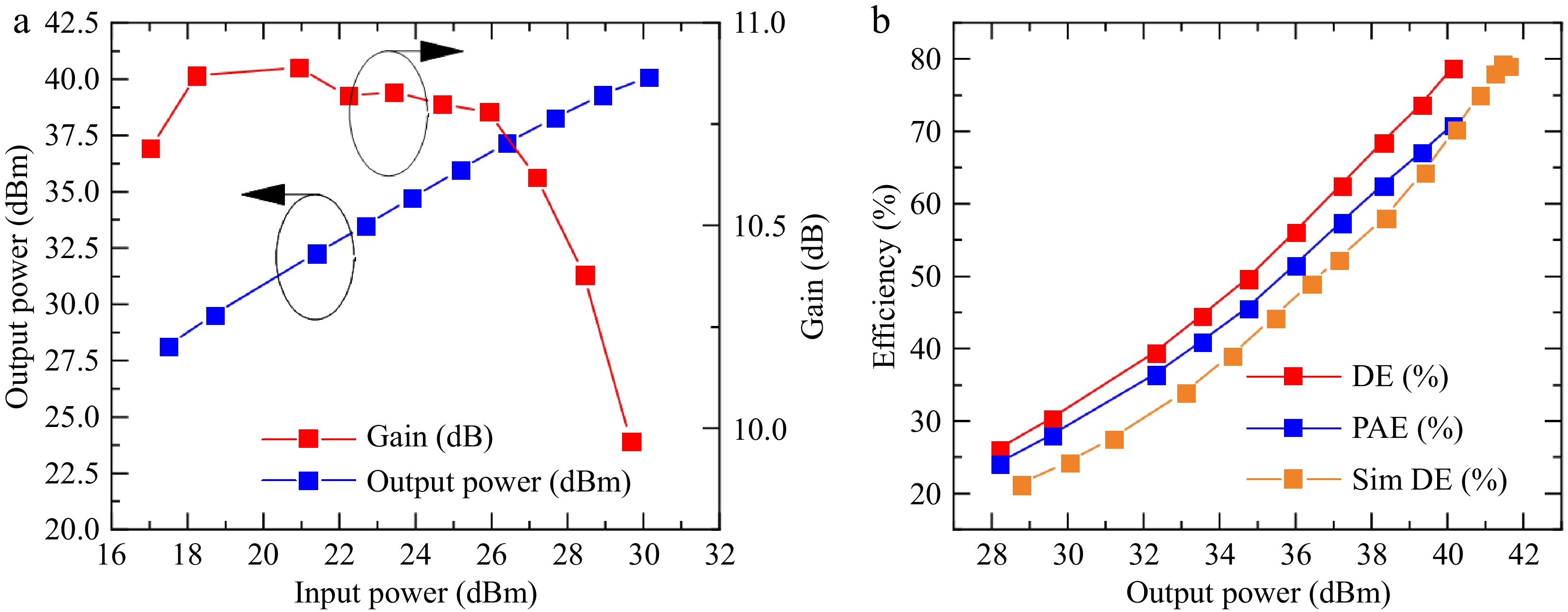
Figure 14.
Measured PA performance. (a) Output power and gain. (b) Drain efficiency and power-added efficiency.
Rectifier performance test
-
A rectifier test system was constructed. In the test, the gate voltage was set to −6.6 V, and the load resistance was 150 Ω. Different input power levels were applied to measure the load voltage and efficiency. The experimental results are shown in Fig. 15. At an input power of 38 dBm, the highest drain efficiency is 85.95% and the output voltage is 28.5 V. When the input power is increased to 40 dBm, the output voltage rises to 34.5 V, but the drain efficiency drops slightly to 79.35%. The experimental trends are generally consistent with the simulation, indicating that the bidirectional system exhibits high power conversion efficiency in the rectifier mode, especially under high-power inputs, and demonstrates good stability and consistency.
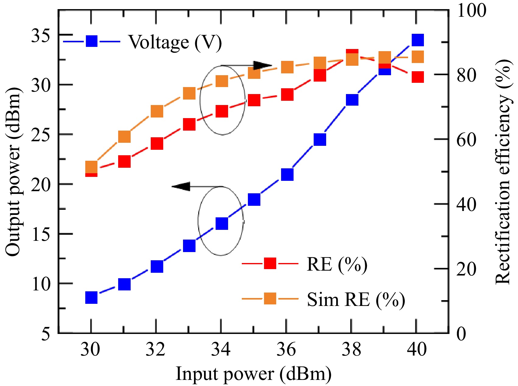
Figure 15.
Measured rectifier performance vs input power.
Overall system performance test
-
To assess the overall performance of the bidirectional system, the microstrip array antennas were fabricated, and a microwave wireless power transfer system was set up. The two fabricated bidirectional circuits were placed on the transmitting antenna and receiving antenna, respectively. The system on the transmitting side operates in PA mode, and the system on the receiving side operates in rectifier mode. By manually switching the operating modes of the bidirectional circuits, bidirectional transfer of microwave wireless power can be achieved. The overall experimental setup is shown in Fig. 16. Experimental tests indicate that the transmitting antenna outputs 40.1 dBm of RF power via the power amplifier. At a transmission distance of 5 m, the receiving antenna receives 31.16 dBm of power, yielding a space transmission efficiency of 12.77%. After the rectifier circuit on the receiving side converts the RF energy into DC power, it successfully powers a 1 W LED.
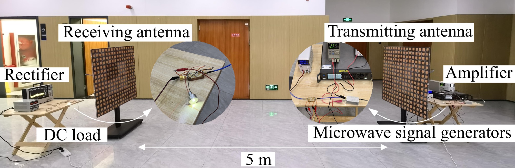
Figure 16.
Scaled-down prototype with bidirectional power transmission at a distance of 5 m.
Table 2 compares the parameters of similar power amplifiers and rectifiers, showing that the proposed integrated module has outstanding performance in both the PA and rectifier modes. The overall test results verify the feasibility of the bidirectional system and the microwave wireless power transfer system, demonstrating its potential application in long-distance wireless power delivery.
Table 2. Benchmarking performance of power amplifiers and rectifiers.
PA
modeRectifier
modeFrequency
(GHz)Power
(dBm)Gain
(dB)DE
(%)RE
(%)Ref. Yes No 2.6 40 12 76 NA [14] No Yes 2.85 40 NA NA 84.94 [18] No Yes 1.85 40 NA NA 83.6 [20] No Yes 2.4 15 NA NA 82.2 [21] No Yes 2.45 31 NA NA 81.3 [22] Yes No 2.6 41.4 10.7 74.7 NA [23] Yes No 1.6 42.5 12.5 82 NA [24] Yes No 2.4 27.4 11.2 82 NA [25] Yes Yes 2.45 40.1 10.1 78.68 85.95 This work -
This paper proposes and implements a bidirectional, wireless power module capable of freely switching between the power amplifier mode and the rectifier mode, realizing DC-RF and RF-DC energy conversion in one module. The bidirectional microwave system enhances component reusability, reduces the system size, and lowers system cost. The final module measures 50.8 mm × 29.7 mm, featuring high integration and practical applicability. Experimental tests show that the module achieves a maximum drain efficiency of 78.68% in the PA mode and a maximum rectification efficiency of 85.95% in the rectifier mode, demonstrating its high efficiency and reliability.
To further verify the feasibility of this system, a microstrip array antenna operating at 2.45 GHz is designed, and a scale-down prototype is fabricated. At a transmission distance of 5 m, the antenna attains a space transmission efficiency of 12.77%, successfully powering a 1 W LED load. The system exhibits high scalability, enabling long-distance and high-power energy transfer by expanding the antenna array and employing multiple bidirectional power conversion modules to accommodate a wider range of application scenarios such as small unmanned aerial vehicles and electric vehicles. Future work will further optimize system performance, improve system efficiency and power level to accelerate the practical adoption of this technology.
This research was funded in part by the National Natural Science Foundation of China (Grant No. 52207010), and in part by the Young Elite Scientists Sponsorship Program by CAST (Grant No. YESS20220659).
-
The authors confirm contribution to the paper as follows: study conception and design: Liu Y, Zhang P, Zhang X; data collection: Liu Y, Wei Y; analysis and interpretation of results: Liu Y, Zhang P, Zhang X; draft manuscript preparation: Liu Y, Zhang P, Chen Z. All authors reviewed the results and approved the final version of the manuscript.
-
The data that support the findings of this study are available from the corresponding author upon reasonable request.
-
The authors declare that they have no conflict of interest. Xian Zhang and Pengcheng Zhang are the Editorial Board members of Wireless Power Transfer who were blinded from reviewing or making decisions on the manuscript. The article was subject to the journal's standard procedures, with peer-review handled independently of these Editorial Board members and their research groups.
- Copyright: © 2025 by the author(s). Published by Maximum Academic Press, Fayetteville, GA. This article is an open access article distributed under Creative Commons Attribution License (CC BY 4.0), visit https://creativecommons.org/licenses/by/4.0/.
-
About this article
Cite this article
Zhang X, Liu Y, Zhang P, Chen Z, Wei Y. 2025. An integrated power conversion system for bidirectional microwave wireless power transfer. Wireless Power Transfer 12: e009 doi: 10.48130/wpt-0025-0003 

An integrated power conversion system for bidirectional microwave wireless power transfer
- Received: 30 December 2024
- Revised: 16 January 2025
- Accepted: 06 February 2025
- Published online: 22 April 2025
Abstract: This paper proposes a bidirectional wireless power conversion system that integrates the functions of a power amplifier (PA) and a rectifier at a frequency of 2.45 GHz. The circuit can freely switch between the PA and rectifier modes, thereby realizing the bidirectional function of the DC-RF and RF-DC energy conversion. A bidirectional microwave wireless power transmission system is constructed based on this module and its performance is experimentally verified. In this study, an inverse-Class-F-based bidirectional circuit operating at a frequency of 2.45 GHz is constructed. Experimental measurements show that the maximum drain efficiency of this module reaches 78.68% in the power amplifier mode, and the maximum conversion efficiency reaches 85.95% in the rectifier mode. The microwave wireless power transfer system successfully supplies power to a load at a distance of 5 m.
-
Key words:
- Microwave wireless power transfer /
- Bidirectional system /
- Power amplifier