


-
Silicon carbide (SiC) devices, with their higher dielectric breakdown electric field strength, can achieve a blocking voltage ten times that of silicon (Si) devices when the thickness of the drift region is the same[1]. At present, 10 kV SiC MOSFET has been verified in many applications[2,3], while the feasibility of applying 15 kV SiC MOSFET in the medium-voltage field has also been widely discussed[4,5].
However, introducing SiC MOSFETs into medium-voltage systems has brought severe challenges to the design of isolated gate driver power supplies (GDPS). On the one hand, GDPS needs to provide a sufficiently high isolation capability; On the other hand, to ensure the reliable operation of SiC MOSFETs under the high dv/dt conditions generated by fast switching in medium-voltage applications, GDPS also needs to have high common-mode transient immunity (CMTI). Minimizing the common-mode current can effectively prevent faults in the control circuit[6].
To enhance the insulation barrier and common-mode interference suppression capabilities of GDPS, researchers have explored various methods. The proposed isolation auxiliary power supply design schemes include four types: optical fiber transmission technology, current mutual inductance technology, transformer technology, and wireless power transfer technology. The Power over Fiber (PoF) technology was proposed by a team from The Ohio State University[7]. This scheme effectively eliminates the main loop coupling capacitance Cps while achieving insulation over 20 kV, and can operate stably at switching speeds greater than 200 kV/μs. However, its output power is only 0.5 W, which makes it difficult to meet the power supply requirements of some high-power modules. The second one is current transformer (CT) technology. In the early days, the team from the University of Texas at Austin introduced a CT-type power supply scheme for 7.2 kV/60 A SiC devices to power the LLC resonant converter[8]. The scheme mentioned by Virginia Tech enables the primary and secondary windings to share a magnetic core, with a power density as high as 6.3 W/in3 and a coupling capacitance as low as 1.67 pF[9,10]. It can achieve stable insulation on the basis of a fixed primary winding and is suitable for a scalable multi-output isolated gate drive power supply. In the latest research, a team from Drexel University powered modular DC solid-state circuit breakers based on CT structures, which can support up to 10 sub-modules[11]. This scheme has a natural multi-output function and is widely used. However, this scheme is highly sensitive to the geometric structure in terms of insulation. Even a slight misalignment of the primary side conductor may reduce the insulation level. The third one is the transformer technology (voltage transformer, VT). This scheme is the most widely used due to its simple structure and control[12−18]. The team from ETH Zurich initially developed an isolated drive power supply based on the E-type VT structure, with dimensions of only 16 mm × 16 mm × 14 mm, a coupling capacitance of 2.6 pF, and a withstand voltage of up to 20 kV[19]. North Carolina State University proposed a scheme using PCB coil-type VT to achieve a coupling capacitance of 2 pF and an insulation voltage of 6 kV[20]. A team from Aalborg University demonstrated a multi-output VT structure, with coupling capacitances of 2.6 and 3.5 pF, respectively[12]. The University of Tennessee proposed a flyback converter based on PCB windings, which passed a 1 h 20 kV DC experiment with a coupling capacitance lower than 2.8 pF[13]. In its subsequent research, a VT-type isolated driving power supply that simultaneously considers insulation, coupling capacitance, and volume was proposed, achieving a partial discharge inception voltage (PDIV) higher than 15 kVrms and an ultra-low coupling capacitance of 1.03 pF. The verification was completed in a 13.8 kV/100 kVA three-phase converter composed of 10 kV SiC MOSFET[14]. However, VT technology still faces challenges in terms of insulation and coupling capacitance optimization: on the one hand, it is necessary to ensure sufficient creepage and electrical clearance to prevent breakdown. On the other hand, although many studies have attempted to reduce the coupling capacitance by decreasing the winding area or increasing the winding spacing, the values are still generally high. Wireless power transfer (WPT) technology, different from current transformers and transformers, has the inherent non-contact power transmission characteristics. It can achieve higher power output than current transformers and lower coupling capacitance than transformers. The team from the University of Texas introduced PCB windings to reduce coupling capacitance, achieving optimization by reducing the overlapping area between the windings and the magnetic core, but it also brought about a relatively large leakage inductance[21]. To meet the insulation requirements, sufficient creepage distance and electrical clearance are reserved in the structure. The team from Virginia Tech University adopted the traditional circular coil WPT structure to achieve an isolated drive power supply with a high output of 120 W and a coupling capacitance of 2.78 pF, and proposed a quantitative insulation design scheme lacking in isolated drives[22,23].
With the increasing demand for advanced insulation techniques in power electronics, recent studies have investigated hybrid structures that integrate WPT and VT technologies to improve both electrical performance and galvanic isolation. One study presents a modeling methodology combined with EMI balancing strategies to suppress common-mode noise in high-voltage SiC switching environments, demonstrating the effectiveness of hybrid-isolated gate driver designs[24]. Another work reports a compact motor drive system that incorporates a WPT-based auxiliary supply and isolated gate drivers, achieving improvements in power density and coupling capacitance[25]. In a separate development, a gate driver power supply capable of operating at 18 kV without partial discharge was achieved through hybrid insulation techniques and magnetic core optimization, offering high PDIV and robust reliability for medium-voltage SiC applications[26]. Furthermore, comparative analysis of integrated planar transformer configurations has been conducted with respect to insulation performance and parasitic suppression, contributing to the structural optimization of WPT/VT-based systems[27].
This paper combines the VT-type and WPT-type isolated drive power supplies by introducing a larger air gap and staggered coil distribution in the traditional transformer to enhance the isolation strength and reduce the coupling capacitance, combined with PCB to achieve a customized coil design. On this basis, the finite element simulation system is adopted to analyze the influence of the shape of the magnetic core and the coil on the isolation performance, explore the role of key structural parameters on the various performances of the isolation unit, and propose a design method that takes into account both isolation performance and parasitic parameter optimization under a compact structure. In addition, a comparative analysis was conducted on different insulating materials and insulating structure schemes, and the initial partial discharge voltages and coupling capacitors of multiple samples were tested through the power frequency partial discharge test platform. The final developed prototype of the isolated drive power supply achieved a partial discharge starting voltage of 21.5 kV effective value, a coupling capacitance of 2.34 pF, and an output power of 20 W.
-
To balance the requirements of medium-voltage SiC MOSFETs for insulation capacity and parasitic parameters, the primary and secondary sides adopt PCB windings that have both insulation capacity and customizability. Its basic structure is shown in Fig. 1a. This structure adopts a magnetic core with an air gap. Compared with the traditional WPT scheme, it can enhance the magnetic coupling of the primary and secondary windings. Compared with the VT scheme, it can prevent the high-voltage side coil from creeping along the surface of the magnetic core to the low-voltage side and causing insulation breakdown. Meanwhile, the primary and secondary coupling capacitance Cps is positively correlated with the relative dielectric constant ε, the effective area S, and the spacing d, as shown in Eq. (1). Therefore, the coupling capacitance under the coil arranged in a side-facing manner is lower than that of the traditional direct-facing coil.
$ C_{\mathrm{ps}}=\dfrac{\varepsilon S}{d} $ (1) 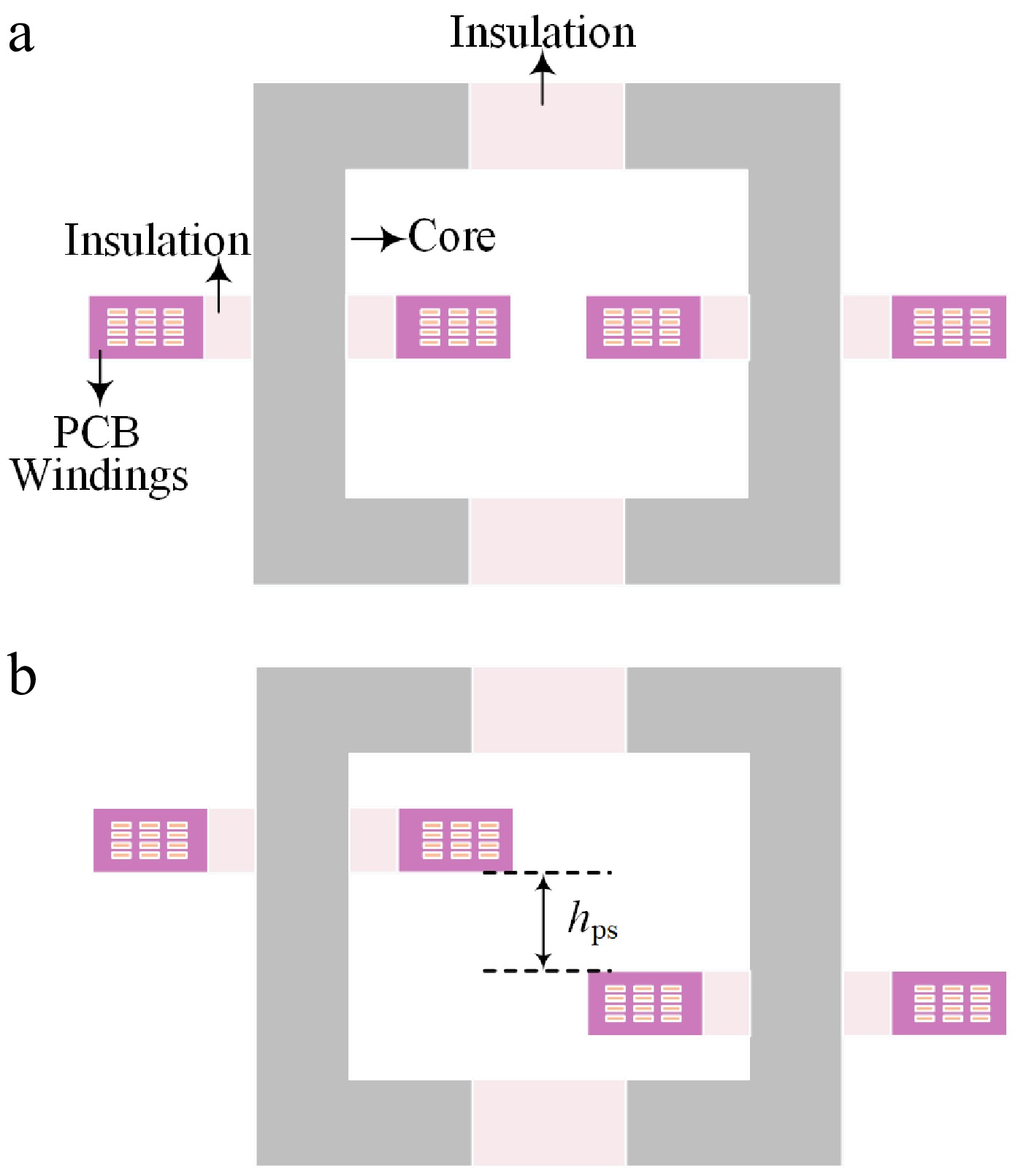
Figure 1.
Derivation of the basic structure of the isolation unit. (a) Not arranged in an alternating pattern. (b) Interlaced arrangement.
Since the magnetic circuit is mainly established by the magnetic core, the staggered arrangement of the primary and secondary side coils does not affect the magnetic field coupling. The structure of the transformer after the staggered arrangement is shown in Fig. 1b. The simulation results of coupling capacitance and maximum electric field intensity are shown in Fig. 2. Both the maximum electric field intensity Emax and the coupling capacitance Cps decrease with the increase of hps.
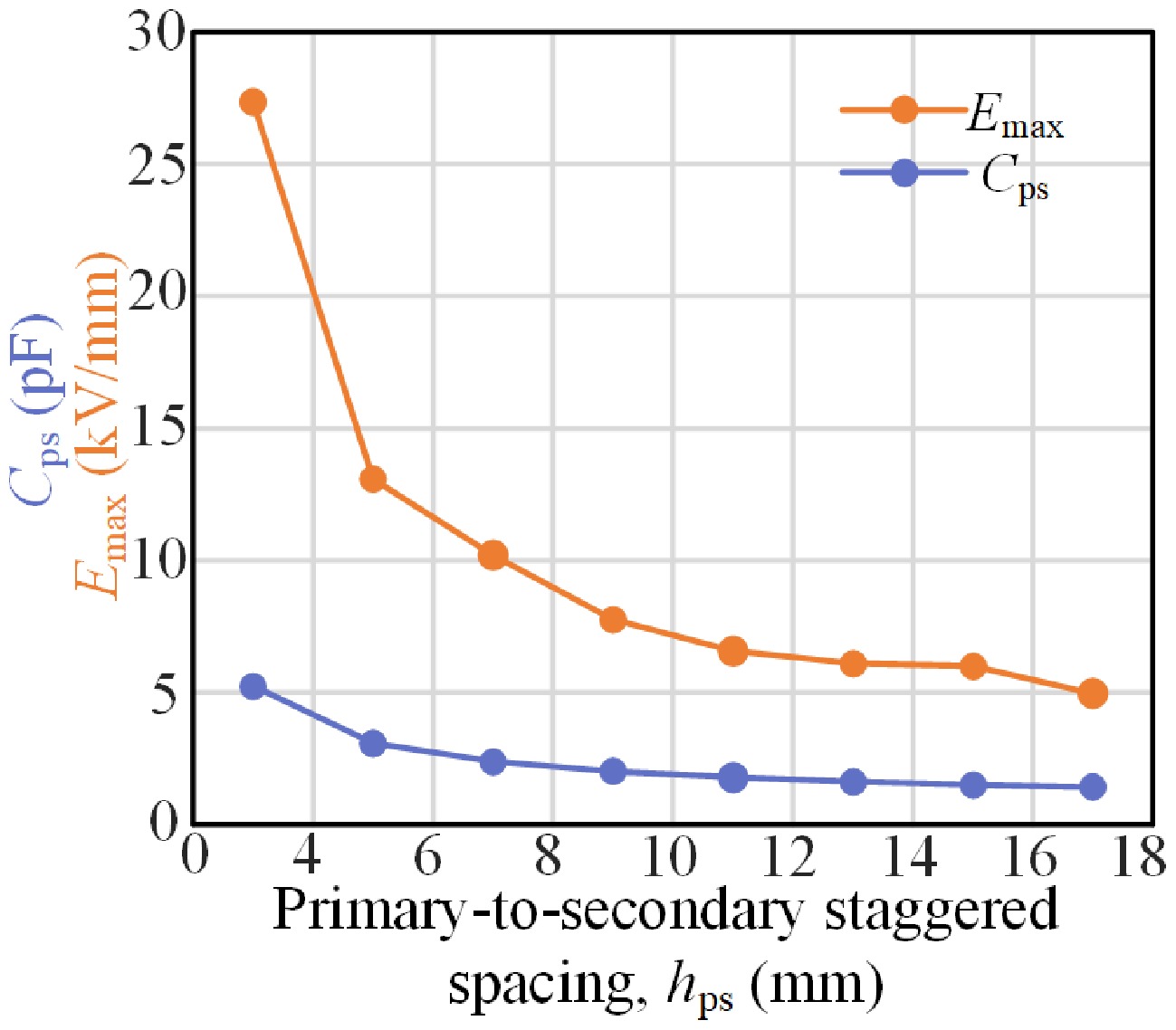
Figure 2.
Impact of hps on coupling capacitor and electric field.
Factors influencing coupling capacitance
-
From the aforementioned analysis, it can be known that the coupling capacitance of the isolated gate drive power supply is closely related to the geometric structure, size, relative position, and distribution of the insulating medium of the isolation unit. To explore the specific influence of key parameters on the coupling capacitance, this paper models and analyzes the capacitance network of the isolation unit. The total capacitance inside the PCB winding (including inter-turn and inter-layer capacitance) is mainly determined by the geometric parameters of the winding itself. Due to its complex mathematical relationship, it will not be discussed separately in this paper. To simplify the analysis, the focus is on the capacitance Ccc between the cores and the capacitance Ctc between the coil and the core, while the influence of the capacitance between turns and between the primary and secondary windings is ignored. The equivalent diagram is shown in Fig. 3.
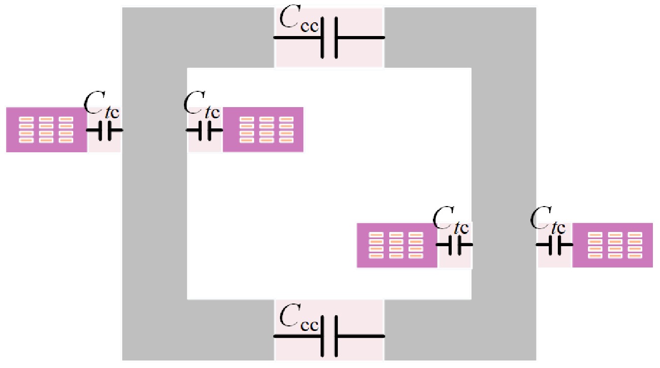
Figure 3.
Parasitic capacitance distribution.
The capacitance Ctc between the winding and the core is shown in Fig. 4. According to the calculation formula of the parallel plate capacitor, the equivalent dielectric constant εeq is
$ \varepsilon_{\text{eq}} = \dfrac{\varepsilon_{\text{FR4}} \varepsilon_0 d_2 + \varepsilon_{\text{in}} \varepsilon_0 d_1}{\varepsilon_0 (d_1 + d_2)}$ (2) where, ε0 is the dielectric constant of the vacuum; εFR4 is the relative dielectric constant of epoxy resin in PCB; εin is the relative dielectric constant of the insulating medium between the core and the PCB; d1 is the distance from the edge of the PCB to the magnetic core; d2 is the distance from the edge of the copper layer to the edge of the PCB.
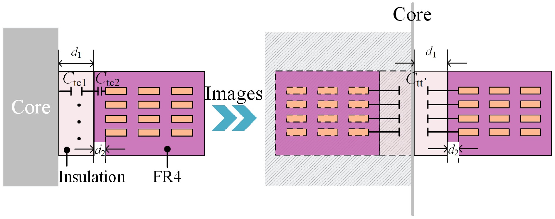
Figure 4.
Mirror image equivalent of the capacitance Ctc between the winding and the core.
The surface of the magnetic core is approximated as the plane of the charged conductor. According to the mirror image method, it can be equivalent to a set of symmetrically distributed virtual windings, thereby simplifying the calculation of the capacitance between the magnetic core and the actual windings. The equivalent capacitance distribution is shown in Fig. 4. If only the innermost winding is considered, the equivalent capacitance between single-layer windings Ctt'0 can be approximately obtained by using the cylindrical capacitance model.
$C_{u'0} = \dfrac{2\pi \varepsilon_{\text{eq}} \varepsilon_0 t}{\ln \left[ (d_1 + d_2 + w_c) / (d_1 + d_2) \right]} $ (3) where, wc represents the width of the coil. Since the potential of each winding layer is almost the same, the total inter-winding capacitance Ctt' is:
$ C_{u'} = N_1 \dfrac{2\pi \varepsilon_{\text{eq}} \varepsilon_0 t}{\ln \left[ \left( d_1 + d_2 + w_c \right) / \left( d_1 + d_2 \right) \right]} $ (4) where, Nl represents the number of coil layers within the PCB.
The distance from the winding to the magnetic core is half of the distance between the two windings after mirroring. It can be obtained that the capacitance Ctc between the winding and the magnetic core is twice the capacitance Ctt' between the windings after mirroring, as shown in Eq. (5).
$C_{{\rm{tc}}} = 2N_1 \dfrac{2\pi \varepsilon_{\text{eq}} \varepsilon_0 t}{\ln \left[ \left( d_1 + d_2 + w_c \right) / \left( d_1 + d_2 \right) \right]} $ (5) It can be concluded that d1 and d2 have an impact on the parasitic capacitance Ctc, while the coupling capacitance Cps is closely related to Ctc. In addition, d1 and d2 respectively represent the distribution of air and FR4 medium, which have a significant influence on the electric field distribution between the winding and the magnetic core. Therefore, d1 and d2 simultaneously affect the coupling capacitance and the electric field distribution.
-
In medium and high voltage applications, cases of surface insulation failure of PCB windings have been reported. To explore its causes, this paper analyzes it through the finite element simulation method and proposes an improvement plan. In the simulation, air and FR4 were used as insulating media. The TX of the primary coil was set to 0 V, the RX potential of the secondary coil was set to 20 kV, and the magnetic core was set to the floating potential. The simulation results are shown in Fig. 5a. Furthermore, in order to achieve efficient and high-precision electric field simulation, it is necessary to select the key areas for the high-precision grid part before the simulation, while for the remaining areas, the accuracy of some parts should be appropriately reduced. The specific simulation Settings are shown in Table 1. FR4 and air were subjected to extremely detailed division, while for other areas where there would be no electric field distribution, a more detailed grid division was carried out.
According to the simulation results, it can be known that the high electric field intensity is mainly distributed near the coil, as shown in Fig. 5b, and the maximum electric field intensity is 6.86 kV/mm. To facilitate the viewing of the electric field distribution characteristics of this area, the area with obvious electric field defects is magnified. Obviously, the three-phase point electric fields at the copper layer boundary and the junction of the copper layer–FR4–air are the most prominent. The electric field intensities in these areas are several times greater than those in the conventional areas.
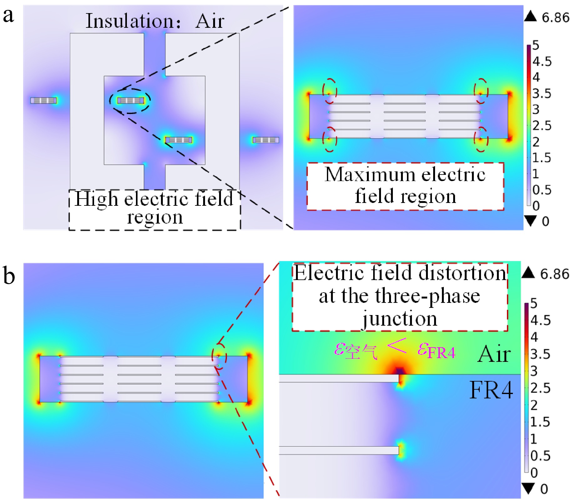
Figure 5.
Electric field distribution in key areas of the isolation unit. (a) Details of the electric field distribution of the isolation unit. (b) Three-phase point distorted electric field.
Table 1. Key parameter settings for finite element simulation of electric field.
Parameter name Numerical value/description TX potential 0 V RX potential 20 kV Magnetic core potential Floated potential Coil mesh partitioning More detailed Core grid division More detailed FR4/Air grid partitioning Extremely detailed Exploring the causes of insulation failure of PCB windings and proposing improvement schemes are crucial for enhancing their insulation performance. The following will respectively analyze the two types of insulation defects and propose suppression methods.
The increase in the electric field intensity at the copper layer boundary is mainly caused by charge accumulation and edge effects. According to Gauss's theorem:
$ \nabla \cdot D=\rho $ (6) $ D=\varepsilon_{0} E+P $ (7) where,
$\nabla $ When the medium is isotropic and linear, the following can be obtained:
$ D=\varepsilon_{0} E+P=\varepsilon_{0}\left(1+\chi_{0}\right) E=\varepsilon_{0} \varepsilon_{\mathrm{r}} E $ (8) where, χe is the polarizability of the medium and ε is the relative dielectric constant of the medium. The relationship between the electric field intensity E and the free volume charge density ρ can be further derived from Eqs (6) and (8) :
$ \nabla \cdot \varepsilon_{0} \varepsilon_{\mathrm{r}} E=\rho $ (9) It is not difficult to find that the electric field intensity is proportional to the volume charge density. In regions with larger curvatures, such as sharp edges or corners, the charge density will increase significantly and is inversely proportional to the radius of curvature r, that is:
$ \rho \propto \dfrac{1}{r} $ (10) However, the radius of curvature at the edge of the copper layer is approximately infinitesimal. This leads to a significant increase in the volumetric charge density. According to Eq. (9), the boundary electric field intensity will increase with the increase of the volume charge density, which explains the problem of the non-uniformity of the boundary electric field.
In addition to the problem of the electric field at the boundary of the copper layer, a more significant electric field distortion will occur at the interface of the three materials: copper, FR4, and silica gel. The cause of this phenomenon can be explained by the connection conditions of the medium interface. According to Maxwell's equations, the tangential component of the electric field intensity E at the interface is always continuous; that is,
$ \varepsilon_{\mathrm{FR} 4} E_{\mathrm{FR} 4}=\varepsilon_{{air }} E_{{air }} $ (11) The relative dielectric constant of FR4 is 4.6, which is significantly higher than that of air, resulting in the electric field intensity on the air side being much higher than that on the FR4 side. However, the dielectric strength of air is much lower than that of FR4. As shown in Fig. 5 and Table 2, the appearance of the three-phase points will significantly intensify the electric field stress of the medium with weak dielectric strength.
Table 2. Key characteristics of common insulating media.
Material Dielectric strength @25 °C Relative dielectric constant Viscosity FR4 45 kV/mm 4.6 − Epoxy resin 18 kV/mm 4.5 2,000 cps Polyurethane 20 kV/mm 3.7 1,600 cps Silicon gel 25 kV/mm 2.8 1,000 cps Air 3 kV/mm 1 − To solve the above problems, in this paper, the copper layer boundary of the PCB coil is homogenized, and the curvature is controlled by adjusting the boundary offsets O1 and O2. As shown in Fig. 6a, the boundary setting is illustrated. When the offsets O1 and O2 are 0.2 mm, the maximum electric field intensity decreases from 6.86 to 4.76 kV/mm (Fig. 6b).
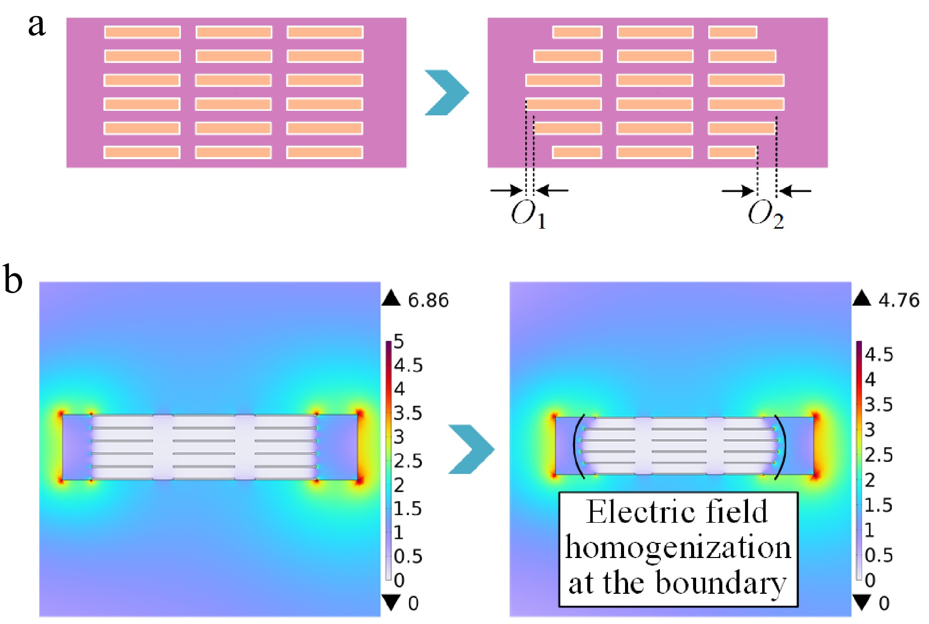
Figure 6.
Boundary electric field homogenization and parameter scanning. (a) Boundary homogenization. (b) Boundary electric field parameter scanning.
Coil AC resistance
-
The main coupling coefficient of the WPT + VT hybrid isolation unit is usually low, which limits power transmission. Although increasing the operating frequency can alleviate this problem, it will intensify the skin effect and proximity effect of the windings, resulting in a significantly higher AC resistance than DC resistance. Therefore, the thickness of the copper layer needs to be reasonably selected to reduce high-frequency copper loss.
According to the Dowell formula[28], without considering the influence of excitation current, the AC resistance Rac and DC resistance Rdc of the multi-layer winding can be expressed as:
$ R_{\text{AC}} = FR \cdot R_{\text{DC}} = FR \cdot \dfrac{\rho \cdot L}{A} = FR \cdot \dfrac{\rho \cdot L}{w_{\text{d}} \cdot t_{\text{copper}}} $ (12) where, ρ is the resistivity of the copper layer, tcopper is the thickness of the copper layer, L is the length of the coil, wd is the width of the coil, and there is an AC coefficient FR:
$ FR = \dfrac{R_{\text{ac}}}{R_{\text{dc}}} = \dfrac{\xi}{2} \left[ \dfrac{\sinh \xi + \sin \xi}{\cosh \xi - \cos \xi} + (2m - 1)^2 \dfrac{\sinh \xi - \sin \xi}{\cosh \xi + \cos \xi} \right] $ (13) In the formula, ξ is the ratio of the winding thickness tcopper to the skin depth δ. Skin depth δ can be expressed as:
$ \delta=\sqrt{\dfrac{1}{\pi f \mu \sigma}} $ (14) where, f is the operating frequency, μ is the magnetic permeability, and σ is the electrical conductivity.
This paper selects a working frequency of 400 kHz and six layers of coils. According to Eq. (12), the copper thickness of the winding simultaneously affects both AC resistance and DC resistance. When the number of layers m and the frequency f are fixed, the relationship between the copper thickness tcopper and the AC coefficient FR is shown in Fig. 7, which reflects its combined influence on the two resistors. The simulation shows that the minimum AC resistance can be obtained when both the primary and secondary coils are 2 oz, that is, when the copper thickness is 70 μm.
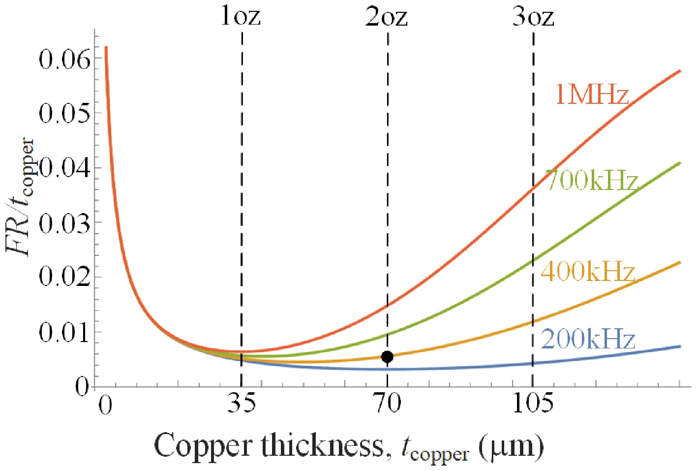
Figure 7.
Relationship between AC coefficient FR and winding thickness of tcopper at different frequencies.
To further evaluate the impact of material parameter variations on simulation results, a sensitivity analysis was conducted on εr by applying ± 5% and ± 10% perturbations in the simulation model. The results indicate that the coupling capacitance varies by no more than 7%, and the position of the maximum electric field shifts by less than 3%. These findings demonstrate that the selected parameter values have a limited influence on the simulation outcome, and the model exhibits sufficient robustness.
Multi-objective optimization process
-
It can be known from the above that the structural parameters d1, d2, and hps affect the electric field distribution and coupling capacitance, and it is difficult to accurately predict their changing trends through mathematical models. Therefore, COMSOL multi-physics field simulation is used to scan d1, d2, and hps, and the maximum electric field intensity Emax and coupling capacitance Cps are solved through the electric field interface. And it is necessary to comprehensively consider the maximum electric field Emax, the coupling capacitance Cps, and the volume V of the isolation unit. The structure of the magnetic core is shown in Fig. 8, and the parameters of the magnetic components are presented in Table 3.
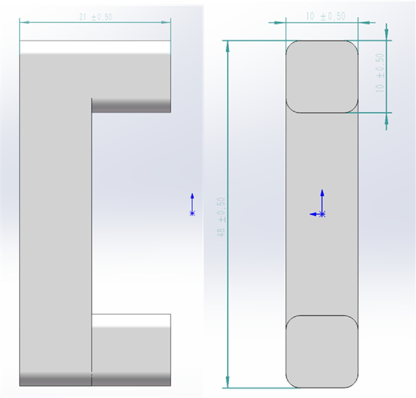
Figure 8.
Core structure.
Table 3. Key parameters of magnetic components.
Parameter name Numerical value Copper layer thickness 70 μm Number of coil layers Six floors Core length 21 mm Core height 48 mm Air gap 4 mm Cross-sectional length of the magnetic core 10 mm The cross-sectional width of the magnetic core 10 mm Coil interlacing spacing hps (3 mm, 8 mm) PCB-Core spacing d1 (0.5 mm, 3 mm) Copper layer-PCB spacing d2 (0.5 mm, 3 mm) The multi-objective optimization process (Fig. 9) consists of four steps:
(1) Global parameter scanning and electric field simulation: Fix other parameters, systematically scan hps, d1, and d2, and simultaneously conduct joint electric field simulation of the isolated unit based on MATLAB + COMSOL;
(2) Extraction of key performance indicators: Extract the maximum electric field Emax and coupling capacitance Cps from the simulation results;
(3) Constraint condition setting: d1 + d2 is set to be less than or equal to 5 mm to ensure compactness. Select the parameter groups that meet the requirements;
(4) Pareto optimization: Select the optimal parameter combination with both Emax and Cps being smaller to determine the final PCB coil design.
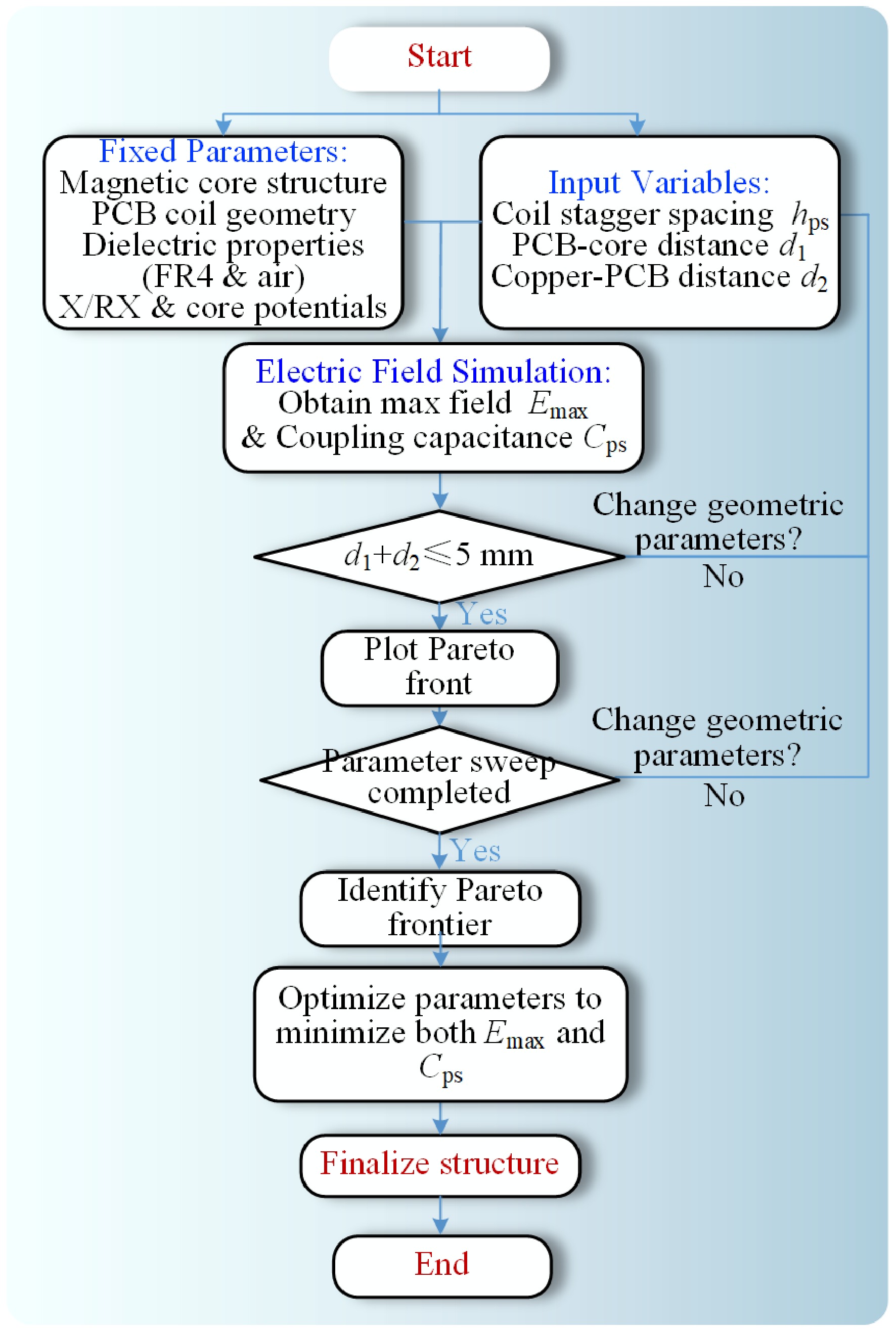
Figure 9.
Multi-objective flowchart.
As shown in Fig. 10a, b, the parameter scanning results of the maximum electric field intensity Emax and the coupling capacitance Cps are presented. In this paper, by making corresponding trade-offs between the two targets, it is finally determined that the coil interleaved spacing hps is 12 mm, the spacing d1 between the PCB and the magnetic core is 2.5 mm, and the spacing d2 between the copper layer and the PCB is 1.5 mm. The selected design achieves the best balance between isolation capability and parasitic parameters.
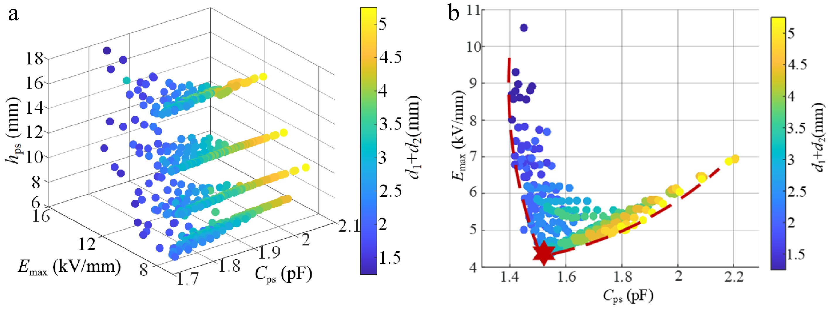
Figure 10.
Multi-objective optimal result. (a) Pareto. (b) Selection of the optimal parameter group.
This section analyzes how key structural parameters—such as coil-to-core spacing, copper edge offset, and coil interlacing—affect electric field distribution and coupling capacitance. Finite element simulations and multi-objective optimization identify a design space that enhances insulation performance while minimizing parasitic effects, forming the basis for subsequent material and packaging improvements.
-
Based on the previous insulation research of the isolation unit, this section investigates the selection and configuration of encapsulation materials to improve insulation performance. Based on simulation-identified electric field hotspots, materials like silicone gel—with high dielectric strength and low permittivity—are chosen to suppress field concentration. Partial and full potting strategies are examined to mitigate peak fields while maintaining low coupling capacitance.
Therefore, in this paper, a partial encapsulation strategy is adopted to separately package the PCB to improve the potential line distribution and reduce the electric field intensity on the air side. Due to the suspension of the magnetic core, its potential is close to but not exactly the same as that of the winding. During the potting process, the dielectric distribution between the magnetic core and the PCB needs to be reasonably controlled to effectively suppress the electric field intensity in this area.
As shown in Fig. 11a, during partial potting, there is only air and silicone gel between the magnetic core and the PCB. The proportion of the air part is e1, and the proportion of the potting part of the PCB is e2, and e1 + e2 = d1. The optimal medium distribution ratio when the electric field intensity is low can be obtained by scanning the parameter e2. It can be known from Fig. 11b that when d1 = 2.5 mm, when the proportion of air e1 is 1.1 mm and the proportion of silicone gel e2 is 1.4 mm, the maximum electric field intensity in the air is the lowest, which is less than its dielectric strength of 3 kV/mm.
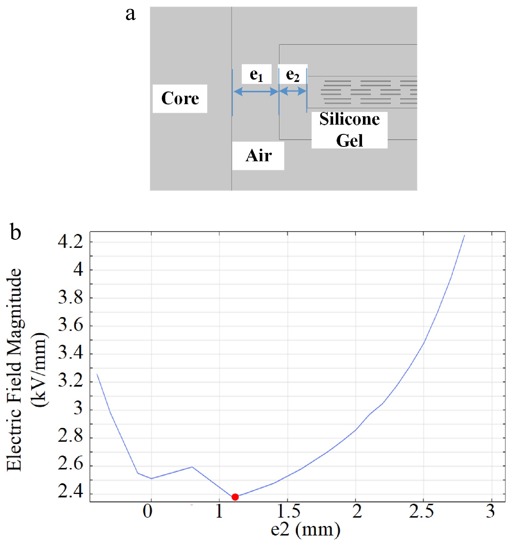
Figure 11.
Optimization of the distribution of insulating medium between the core and PCB during partial glue filling. (a) Schematic diagram of the distribution of partial sealing and filling media. (b) Medium distribution scanning results.
In addition to the potting process, covering the surface of the magnetic core with insulating tape can also effectively alleviate the concentration of the electric field in the sharp corner areas. Thin-layer NOMEX paper or polyimide film can be selected as an insulating material. Among them, the dielectric constant of NOMEX paper is lower than that of epoxy resin and closer to air, which is conducive to forming a uniform electric field distribution, thereby suppressing partial discharge and delaying insulation aging.
This section proposed and evaluated two insulation enhancement strategies—partial and full encapsulation—based on prior electric field distribution simulations. By adjusting the distribution of air and gel within critical regions and considering the use of insulating surface films, the insulation strength can be significantly improved while partially preserving low coupling capacitance. These design strategies were validated through experimental tests in the next section.
-
To verify the insulation performance of the half-bridge isolated drive power supply, a partial discharge test platform was built in this paper, and the device is shown in Fig. 12. The platform adopts the pulse current method to detect partial discharge. The main components include: 220 V AC input, no partial discharge voltage stabilizing console, 10 kVA filter, 10 kVA/100 kV test transformer, 100 kV/5 kΩ high-voltage protection resistor, 100 kV/800 pF coupling capacitor, and partial discharge monitoring equipment GDJF 2008 series. The platform can output a maximum power frequency voltage of 50 kVrms and 50 Hz, with a capacity of 10 kVA, and is used to measure the initial voltage of partial discharge and apparent discharge quantity.
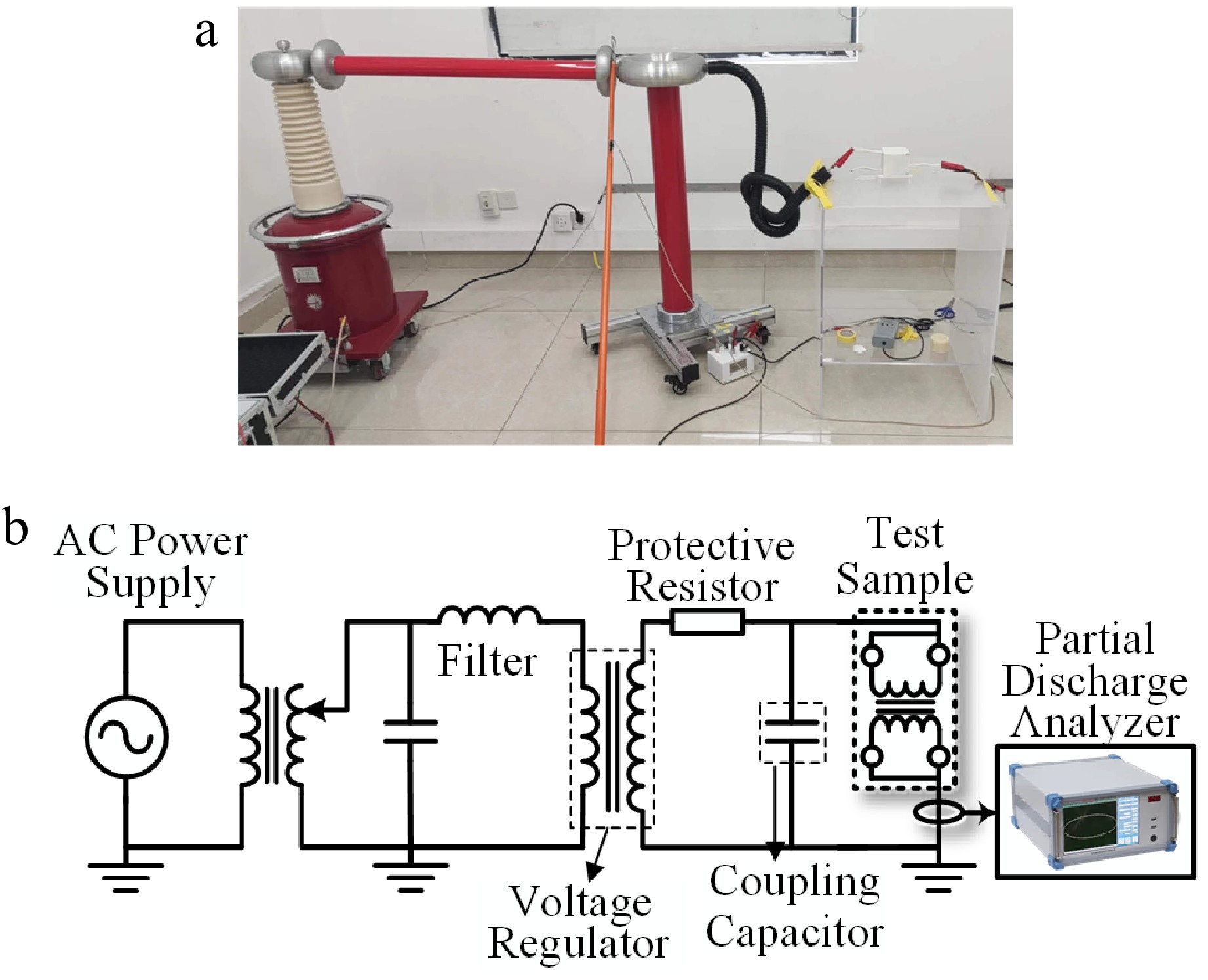
Figure 12.
(a) Partial discharge device and (b) partial discharge test schematic diagram test principle.
The designed isolated drive power supply is shown in Fig. 13. In the local potting scheme, the acrylic sheet is used as the bracket, and only the PCB part is potting and fixed. The overall encapsulation solution uses a closed ABS printed shell as the container to achieve the overall encapsulation of the isolation unit.
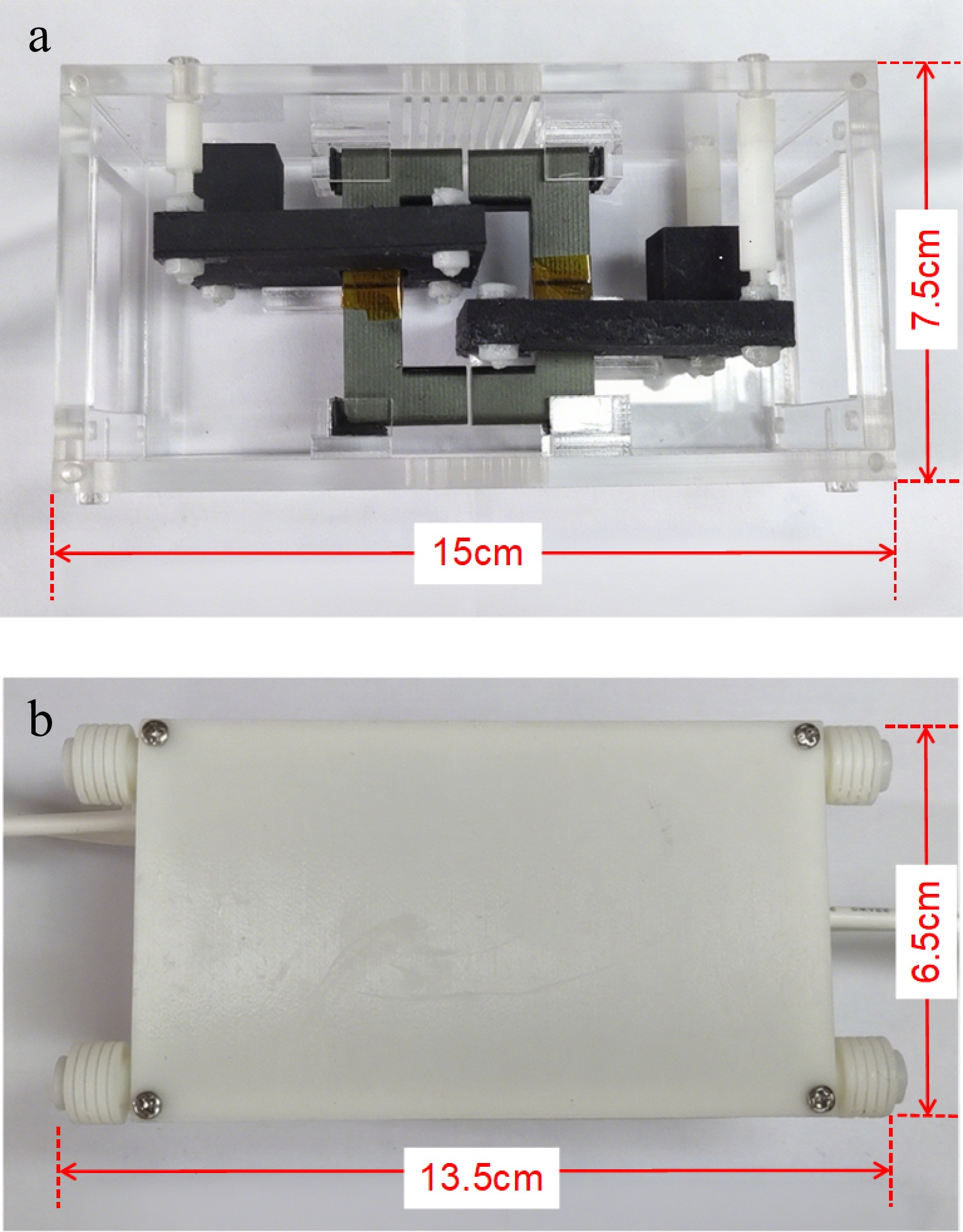
Figure 13.
Isolation unit samples under different sealing schemes. (a) Local sealing and filling. (b) Overall sealing and filling.
Figure 14a, b shows the partial discharge test results of some potting isolation units. The PDIV is located between 7.5 and 8 kVrms. Figure 14c, d shows the test results of the overall sealing and irrigation isolation unit, with the PDIV ranging from 21.5 to 22 kVrms. These results indicate that the isolation ability of the overall potting sample is superior to that of the partial potting sample. This might be caused by reasons such as the lower dielectric strength of the air and the incomplete elimination of bubbles in the potting cavity.
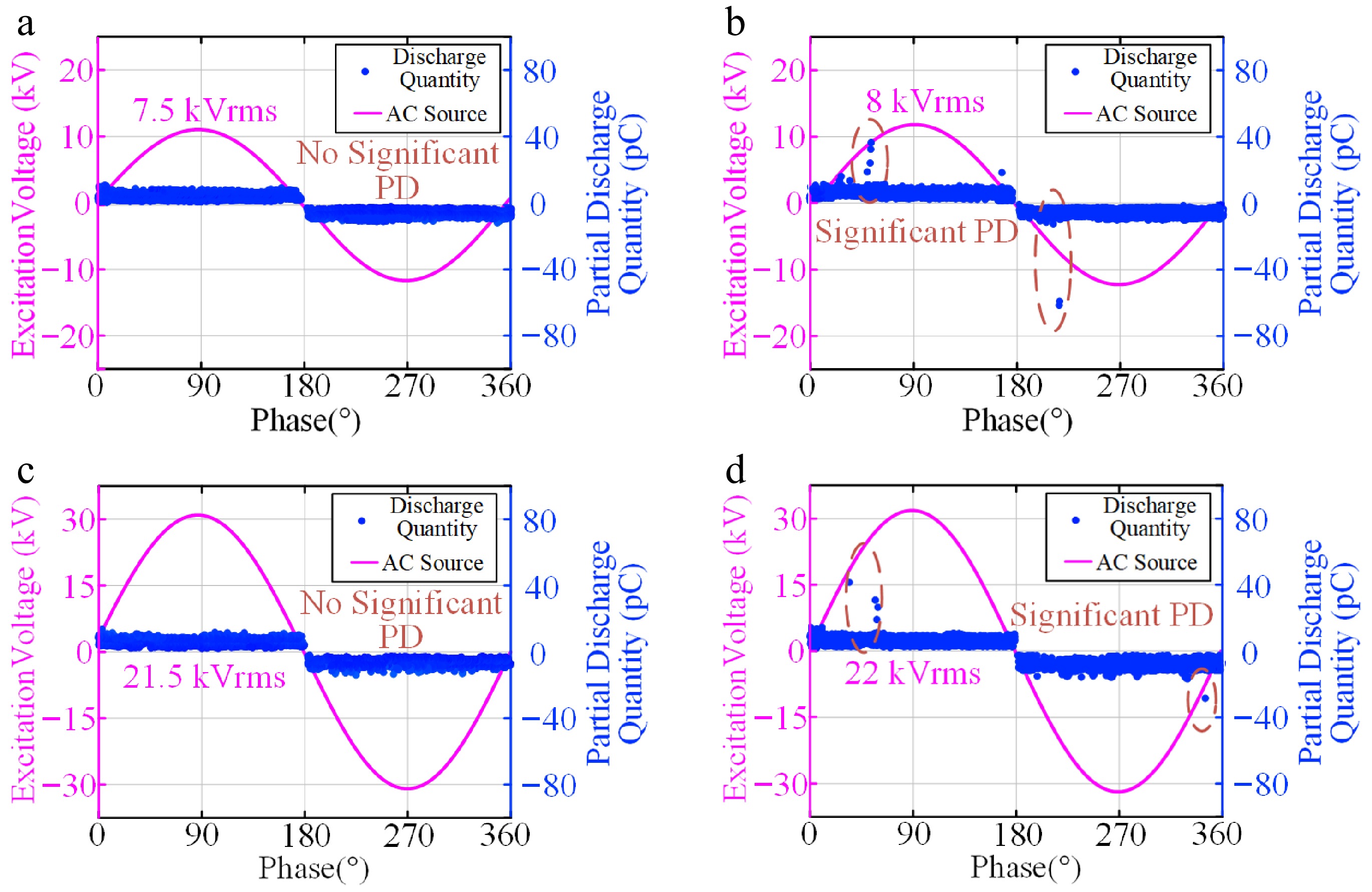
Figure 14.
PDIV levels of isolation units under different sealing schemes. Partial discharge test of local sealing and filling under a voltage of (a) 7.5 kVrms, (b) 8 kVrms, (c) 21.5 kVrms, (d) 22 kVrms.
Coupling capacitance experiment
-
The test results of the coupling capacitance under different potting schemes are shown in Fig. 15. The local potting sample is 1.65 pF, and the overall potting sample is 2.34 pF. Although there are differences in the proportion of insulating adhesives, due to the small differences, the change in coupling capacitance is not significant.
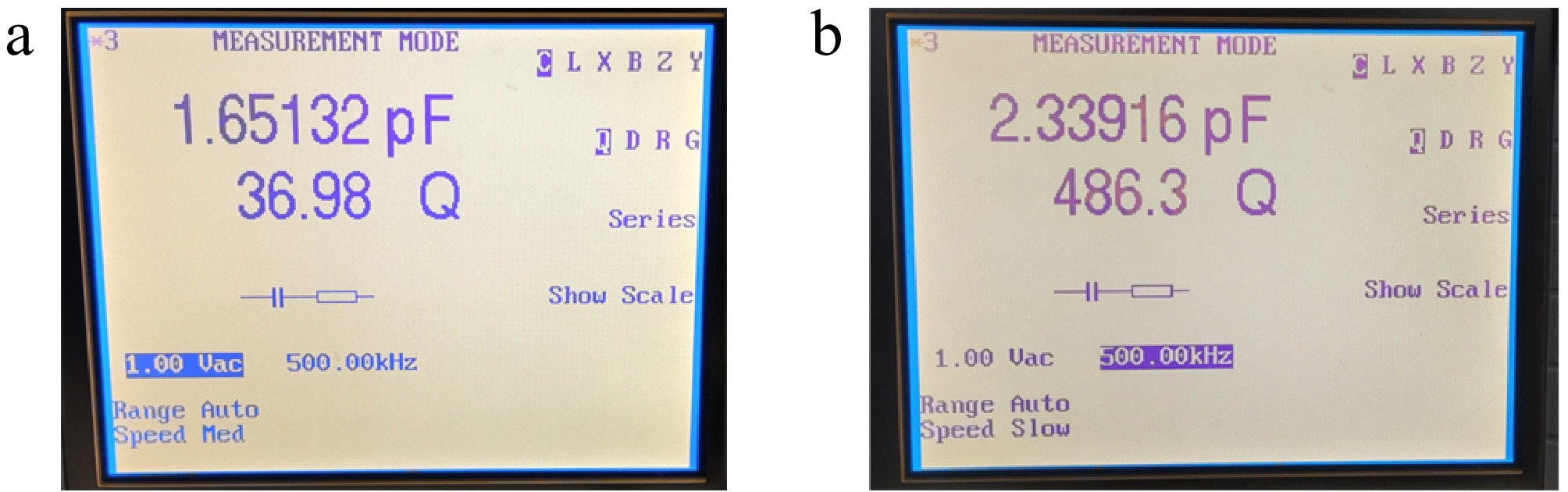
Figure 15.
Coupling capacitor experiment under different sealing schemes. (a) Test data of local sealing and filling. (b) Test data of overall sealing and filling.
Based on the test results of isolation capacity and coupling capacitance under different potting schemes, the overall potting is significantly superior to partial potting in isolation performance, and the coupling capacitance is only slightly higher. According to the IEEE Std.C57.12.01-2020 standard, the PDIV of dry-type transformers of 10 kV and above should not be lower than 18.75 kV. Given the small difference in coupling capacitance between the two, this paper finally selects the overall potting and filling scheme with stronger isolation ability for the design of the isolated drive power supply.
Prototype construction and output testing
-
The proposed prototype of the half-bridge isolated driver power supply is shown in Fig. 16. To adapt to the high-frequency switching application, the primary side switching tube selects GS61004B from GaN Systems, while the driver chip is the NCP51810 from ON Semiconductor, which provides an adjustable dead-time function. To achieve a fixed switching frequency, the LTC6908 waveform generator from ADI is adopted, and the set frequency is 400 kHz.
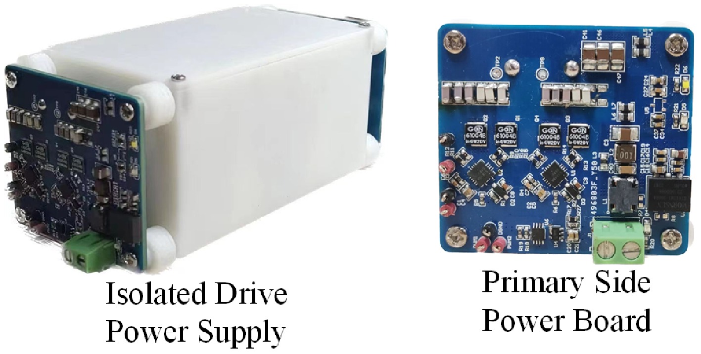
Figure 16.
Proposed prototype.
The winding adopts the resin process of through-hole plugs to avoid the residual air bubbles in the through-holes. The magnetic core is made of Dongci's manganese-zinc ferrite material DMR51W, which features low and high frequency loss characteristics. The sealing and filling material is Ausbon two-component silicone gel.
The full-load output waveform of the isolated drive power supply is shown in Fig. 17. When the rated input voltage is 24 V, the output power can reach 20 W, meeting the driving power requirements of most medium-voltage devices. The specific parameters of the proposed isolated drive power supply are shown in Table 4.
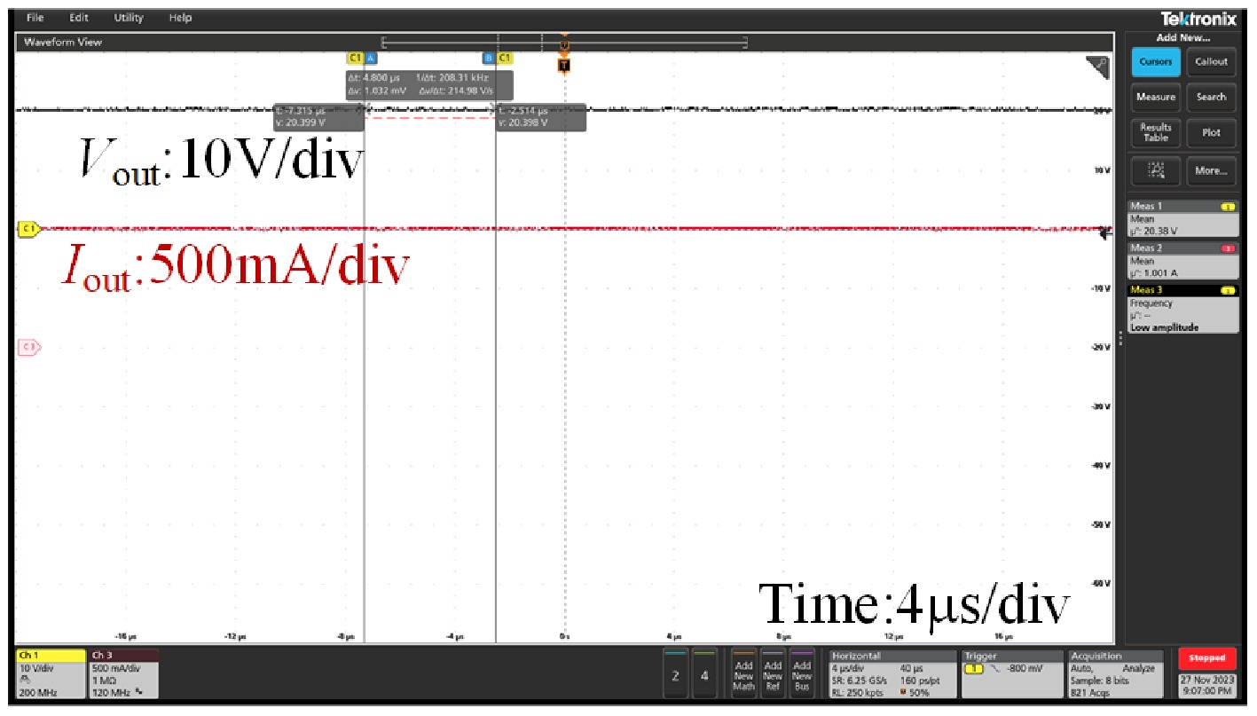
Figure 17.
Isolation drive voltage, output voltage, and current waveform.
Table 4. Isolate the key parameters of the drive power supply.
Parameter name Numerical value Number of turns of the primary side coil n1 20 Number of turns of the secondary side coil n2 20 Self-induction of the primary side coil L1 47.2 mH Self-induction of the secondary side coil L2 47.2 mH The mutual inductance between the primary and secondary coils M 12.7 mH Coupling coefficient k12 0.27 Switching frequency fsw 400 kHz Output power Pout 20 W Isolation voltage level 21.5 kVrms -
Table 5 summarizes the existing multi-output isolated drive power supply solutions, including the solution for a medium-voltage half-bridge isolated drive power supply. The isolated drive power supply proposed in this paper outperforms the scheme based on current transformers in terms of isolation performance, surpasses the design based on wireless power transmission in terms of power transmission capacity, and significantly reduces the coupling capacitor compared to other schemes based on loosely coupled transformers. The achieved PDIV exceeds 18.75 kV, leaving sufficient margin and achieving a level of isolation that is incomparable to the existing multi-channel isolated drive power supplies. In addition, this design also ensures strong isolation between the two secondary coils.
Table 5. Performance comparison of existing multi-output isolated power supply.
Materials and
insulation strategyPDIV Cps Pout Ref. Air insulation, no encapsulation > 33 kV (no
obvious discharge)2.76 pF 2*60 W [22] Silicone + NOMEX + local encapsulation structure 21.5 kVrms
(effective value)2.34 pF 2*20 W This paper -
This paper aims to address the contradiction between high isolation capability and low coupling capacitance in the isolated gate drive power supply of medium-voltage silicon carbide power devices, and proposes and verifies a design of a loosely coupled transformer isolated drive power supply based on WPT. By establishing the theoretical model of coupling capacitance and conducting parameter analysis, the key factors affecting the balance between isolation performance and coupling characteristics were clarified. The innovative introduction of electric field boundary homogenization technology effectively alleviates local electric field concentration and enhances the reliability of electrical isolation. Combined with multi-objective optimization, the collaborative optimization of isolation capability and coupling capacitance under a compact structure has been achieved. By comparing insulating materials with packaging schemes, two schemes, local potting and overall potting, were designed, and their performances were verified in the prototype test. Ultimately, the overall potting and sealing scheme performed excellently in terms of the partial discharge starting voltage (21.5 kV), coupling capacitance (2.34 pF), and output power (20 W), verifying the effectiveness and engineering application value of the design scheme.
-
The authors confirm contribution to the paper as follows: study conception and design: Xiao K, Chen Q; data collection: Cai Z, Zheng Q; analysis and interpretation of results: Zhang F, Feng H; draft manuscript preparation: Xiao K, Zheng R. All authors reviewed the results and approved the final version of the manuscript.
-
All data generated or analyzed during this study are included in this published article.
-
The authors declare that they have no conflict of interest.
- Copyright: © 2026 by the author(s). Published by Maximum Academic Press, Fayetteville, GA. This article is an open access article distributed under Creative Commons Attribution License (CC BY 4.0), visit https://creativecommons.org/licenses/by/4.0/.
-
About this article
Cite this article
Xiao K, Chen Q, Cai Z, Zheng R, Zhang F, et al. 2026. Research on the design method of high isolation and low parasitic parameters for medium-voltage SiC MOSFET driver power supply using wireless power transfer. Wireless Power Transfer 13: e001 doi: 10.48130/wpt-0025-0030 

Research on the design method of high isolation and low parasitic parameters for medium-voltage SiC MOSFET driver power supply using wireless power transfer
- Received: 01 July 2025
- Revised: 25 July 2025
- Accepted: 07 August 2025
- Published online: 13 January 2026
Abstract: For medium-voltage SiC devices, there is a mutual restraint between the isolation capability and the coupling capacitance of the isolated gate drive power supply. It is the major bottleneck for structural compactness and insulation reliability. This paper innovatively proposes a loosely coupled transformer design scheme using wireless power transfer, achieving the collaborative optimization of high isolation performance and low coupling capacitance within a limited space. The research first establishes a theoretical model of coupling capacitance. Through parameter analysis, the key design variables that affect the performance of the isolation unit are identified. At the coil structure design level, the electric field boundary homogenization was introduced, significantly reducing the local electric field stress and solving the problem of electric field concentration at the triplet points. Furthermore, this paper conducts an in-depth comparison of different insulating materials and insulation schemes, and proposes two isolation unit design schemes: local potting and overall potting. After verification through partial discharge tests and coupling capacitor performance tests, it was finally determined that the overall sealing and filling scheme was the optimal design. This scheme achieves a partial discharge inception voltage (PDIV) of 21.5 kV effective value, and a low coupling capacitance of 2.34 pF.
-
Key words:
- Wireless power transfer /
- SiC devices /
- Gate driver power supply