












-
Combining advanced modeling and analysis methods, wireless power transfer (WPT) technology effectively addresses the issue of unsafe and inflexible access associated with conventional charging methods[1−5]. To increase the efficiency and power transfer capability of the WPT system, the existing research generally adopts two basic methods: improving the compensation structure and its parameter design method[6,7]; optimize the electromagnetic coupling structure[8,9]. The first method can raise the system output power, realize constant voltage or current output, suppress high-order harmonics, and reduce the reactive power component of the input. The second method has advantages in increasing the efficiency and power density, improving the misalignment ability, maintaining the system security, and reducing the system cost.
Four typical compensation topologies (S/S, S/P, P/S, and P/P) were utilized to improve the performance of inductive power transfer (IPT) systems, but they are prone to load sensitivity issues[10]. Regarding capacitive power transfer (CPT) systems, the coupler can be equivalent to two series coupling capacitors or six cross-coupling capacitors[11,12]. In centimeter-range power transmission applications, the method of using a large inductance for series reactive power compensation comes at the expense of system security and environmental adaptability[13]. In response to the challenges faced by IPT and CPT systems, a range of high-order compensation topologies, such as LCL (inductor capacitor inductor), LCC (inductor capacitor capacitor), CLC (capacitor inductor capacitor), and LCLC (inductor capacitor inductor capacitor), have been proposed. This paper presents a novel parameter tuning method based on an LCL compensation topology. The proposed approach provides enhanced flexibility in the design of IPT systems, along with improved suppression of higher-order harmonics and a reduction in coil current[14]. A dual-side LCC compensation topology along with its resonant scheme has been designed to ensure that the resonant frequency of the IPT system remains immune to variations in coupling coefficient and load, thereby maintaining stable and predictable operation[15]. A π-CLC compensation structure at the transmitter and T-CLC compensation structure at the receiver are adapted in the CPT system, which achieves constant current output when switching between multiple receivers[16]. To minimize the voltage stress imposed on the coupler to enable high-efficiency power delivery across long distances, a CPT system with double-sided LCLC compensation structure is put forward[17]. To continuously improve WPT system performance, scientists have carried out in-depth studies on electromagnetic coupling structures. A significant amount of focus has been placed on the development of a hybrid inductive and capacitive WPT (HWPT) system[18]. A novel HWPT system is presented that achieves a favorable trade-off between enhanced efficiency and a compact coupler design[19]. In addition, an inductive and capacitive integrated coupler, made up of bent aluminum plates, is introduced[20], offering a novel concept and approach for wireless charging. A 10 kW HWPT system exhibits a significant performance advantage, outperforming both previously published IPT and CPT systems across a range of misalignment conditions[21]. However, all of the above couplers have to be compensated by high-order network. In general, the magnetic-field coupler is typically constructed from Litz wire, whereas the electric-field coupler is composed of metal plates. To enhance performance, Litz wire, metal plates, and high-order compensation topologies are often incorporated. However, this approach comes at the expense of greater volume, weight, and cost, creating a critical barrier for WPT technology's progress and market adoption. In conclusion, the majority of existing research has focused on enhancing the output power, the efficiency, and the transfer distance of WPT systems, while neglecting the concomitant increases in volume, weight, and cost.
Aimed at resolving the problems outlined previously, this study puts forward a novel integrated copper-foil electromagnetic coupler and a comprehensive methodology for its modeling and decoupling. Fabricated from copper foil, the four planar square spiral coils that constitute the electromagnetic poles are designed with the objective of alleviating the skin effect, consequently minimizing ohmic losses. Cross-coupling is generated among the four copper-foil coils; consequently, mutual inductances and cross-coupling capacitors are established. Compared with the previous research work, the proposed hybrid electromagnetic coupler is very lightweight and low cost, and the WPT system is very simple and practical for electric vehicle. The remainder of this paper is organized into the following sections. This paper first introduces the coupler structure and its decoupled model. The equivalent circuit of the coupler is analyzed and simplified, and the couplers' inherent electrical parameters are designed to make it self-resonance. Then the working conditions of both load-independent constant current (CC) or constant voltage (CV) output and input ZPA are obtained. In the following, the structure of the coupling electromagnetic pole is optimally designed based on Maxwell to balance the electric field and the magnetic field, and an efficient and portable electromagnetic coupler is constructed. Simulation and experimental results validating the proposed coupler and WPT system are discussed in verification part, concluding with the findings in the end.
-
As shown in Fig. 1, the electromagnetic poles of the proposed coupler take the form of square spiral windings fabricated from copper foil. By leveraging the previously ignored parasitic capacitance of the coil, a significant improvement in power transmission performance can be achieved. Under the influence of both electric and magnetic fields, this coupler inherently integrates a combination of self-inductance, mutual inductance, and cross-coupling capacitor. The three-dimensional model of the copper-foil electromagnetic coupler is presented in Fig. 1a. Its key components are four planar square spiral electromagnetic poles and an insulating dielectric layer. Figure 1b depicts the front view of the copper-foil electromagnetic coupler, where the four electromagnetic poles and insulating dielectrics are stacked. Electromagnetic pole P1, dielectric D1, electromagnetic pole P2, electromagnetic pole P4, dielectric D2, and electromagnetic pole P3 are lined successively from bottom to top. l1 is the side length of P1 and P3, while l2 is the side length of P2 and P4. dt and ds are the transfer distance and the distance between the same-side electromagnetic poles (also the thickness of the dielectric), respectively.
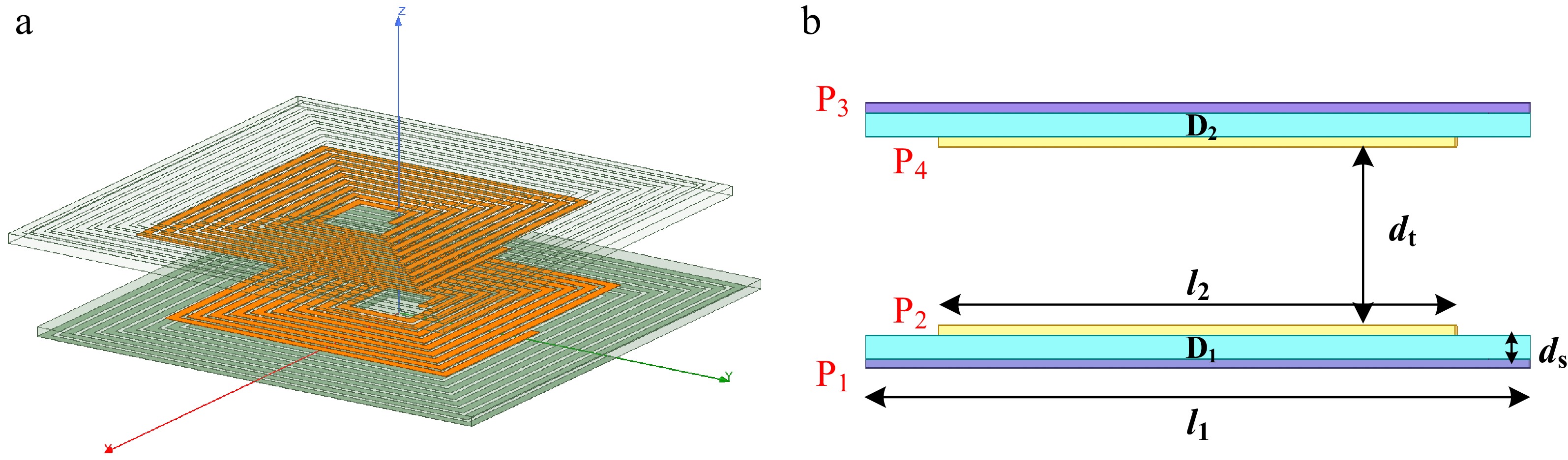
Figure 1.
Basic structure of the copper-foil electromagnetic coupler. (a) 3D graph of the coupler. (b) Front view[22].
System circuit topology and its equivalent simplification
-
With a view to structural simplification, this WPT system deliberately omits any additional compensation components. The copper-foil electromagnetic coupler utilizes its inherent capacitance and inductance characteristics to achieve self-resonant. A schematic illustration of the non-compensated circuit configuration is achieved in Fig. 2, where leakage field reduction is achieved by connecting the inner electromagnetic pole P2 to the inverter's high-potential output terminal and the outer electromagnetic pole P1 to the low-potential output terminal[23]. For simplicity, the circuit characteristics are analyzed employing the Fundamental Harmonic Approximation (FHA), with ohmic losses in the coupler omitted. Due to the equivalence between the six-capacitor cross-coupling and three-capacitor π-type models[24], the circuit from Fig. 2 can be simplified as depicted in Fig. 3, where
$ {U}_{\text{in}}\left({U}_{\text{in}}={U}_{\text{dc}}\cdot \text{4/}\pi \right) $ $ {R}_{\text{eq}}\left({R}_{\text{eq}}={R}_{L}\cdot 8/{\pi }^{2}\right) $ 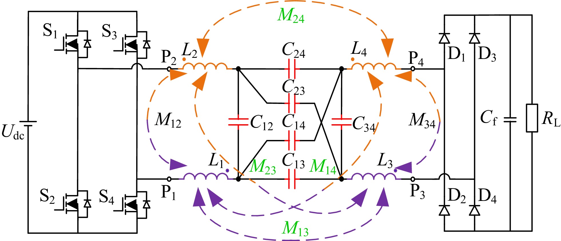
Figure 2.
Circuit topology of WPT system without compensation.
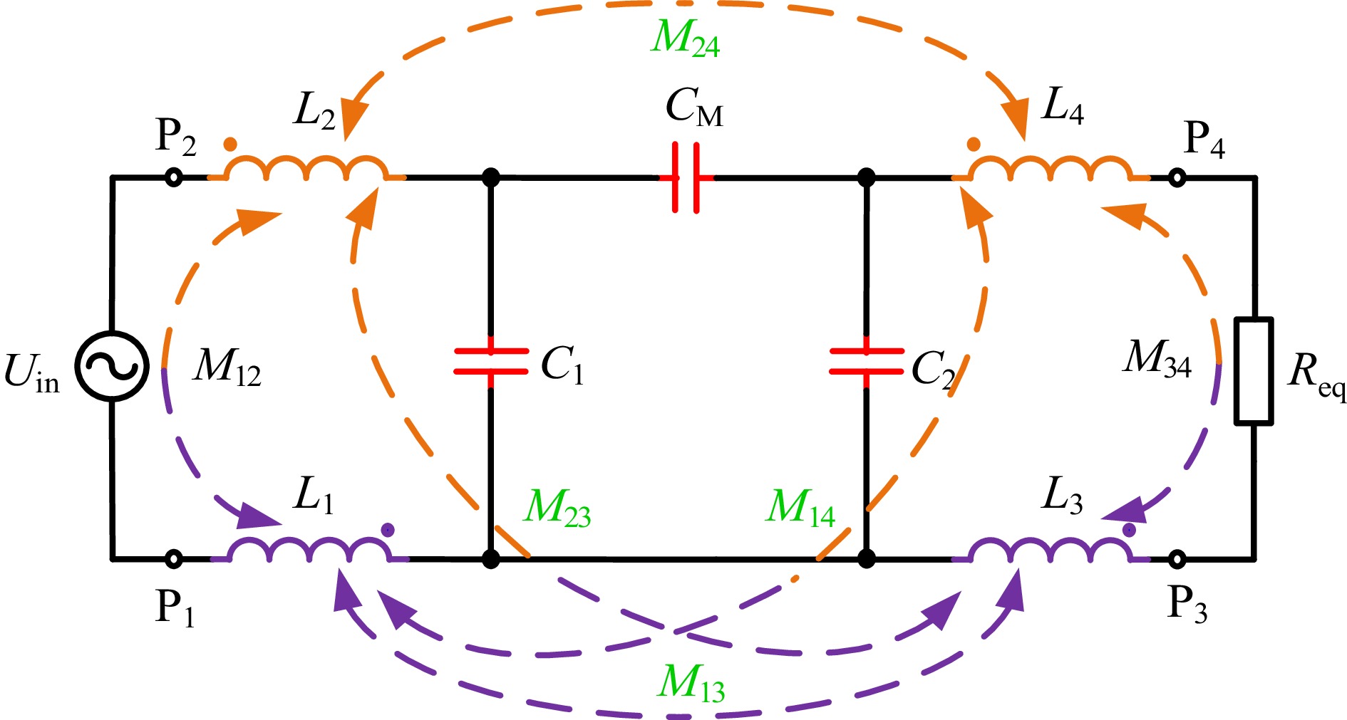
Figure 3.
System π-type equivalent model.
$ \begin{split}&C_{M}=\dfrac{{C}_{\text{13}}\cdot {C}_{24}-{C}_{\text{13}}\cdot {C}_{24}}{{C}_{23}+{C}_{24}+{C}_{\text{13}}+{C}_{14}}\\ & {C}_{1}\text={C}_{\text{12}}-{C}_{M}+\dfrac{\left({C}_{\text{13}}+{C}_{14}\right)\cdot \left({C}_{\text{23}}+{C}_{24}\right)}{{C}_{\text{13}}+{C}_{14}+{C}_{23}+{C}_{24}}\\ & {C}_{2}\text={C}_{34}-{C}_{M}+\dfrac{\left({C}_{\text{13}}+{C}_{14}\right)\cdot \left({C}_{14}+{C}_{24}\right)}{{C}_{\text{13}}+{C}_{14}+{C}_{23}+{C}_{24}} \end{split} $ (1) The electric field coupling coefficient is expressed as:
$ k\mathrm{_{CPT}}=\dfrac{C_M}{\sqrt{\left(C_1+C_M\right)\cdot\left(C_2+C_M\right)}} $ (2) According to the reciprocity theorem, the π-type capacitor network composed of
$ {C}_{\text{1}} $ $ {C}_{\text{2}} $ $ {C}_{M} $ 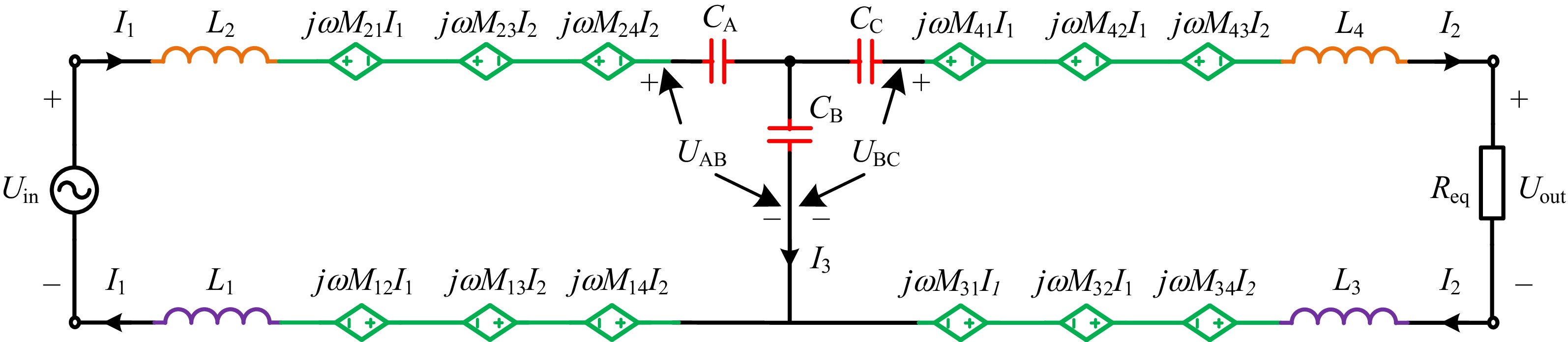
Figure 4.
Controlled source equivalent circuit.
$ \begin{cases} {C}_{A}={C}_{1}+{C}_{M}+\dfrac{{C}_{1}\cdot {C}_{M}}{{C}_{2}} & {C}_{\text{1}}=\dfrac{{C}_{A}\cdot {C}_{B}}{{C}_{A}+{C}_{B}+{C}_{C}}\\ {C}_{B}={C}_{1}+{C}_{2}+\dfrac{{C}_{1}\cdot {C}_{2}}{{C}_{M}} & {C}_{2}=\dfrac{{C}_{B}\cdot {C}_{C}}{{C}_{A}+{C}_{B}+{C}_{C}}\\ {C}_{C}={C}_{2}+{C}_{M}+\dfrac{{C}_{2}\cdot {C}_{M}}{{C}_{1}} & {C}_{M}=\dfrac{{C}_{A}\cdot {C}_{C}}{{C}_{A}+{C}_{B}+{C}_{C}} \end{cases} $ (3) Based on Kirchhoff's law, the input and output voltage can be expressed as:
$ \begin{cases} {U}_{\text{in}}=\text{j}\omega {L}_{2}{I}_{1}+\text{j}\omega {M}_{21}{I}_{1}+\text{j}\omega ({M}_{23}+{M}_{24}){I}_{2}\\ \qquad+{U}_{A\mathrm{B}}+\text{j}\omega {L}_{1}{I}_{1}+\text{j}\omega {M}_{12}{I}_{1}+\text{j}\omega ({M}_{13}+{M}_{14}){I}_{2}\\ {U}_{\text{aa}}=-\left[\text{j}\omega {L}_{2}{I}_{2}+\text{j}\omega ({M}_{41}+{M}_{42}){I}_{1}+\text{j}\omega {M}_{34}{I}_{2}+{U}_{\text{BC}}\right]\\ \quad\qquad-[\text{j}\omega {L}_{3}{I}_{2}+\text{j}\omega ({M}_{31}+{M}_{32}){I}_{1}+\text{j}\omega {M}_{34}{I}_{2}] \end{cases} $ (4) By substituting I1 − I3 for I2, the input voltage can be simplified as:
$ \begin{split}U_{\text{in}}=\; & \text{j}\omega I_1(L_2+M_{21}+M_{23}+M_{24}+I_1+M_{12}+M_{13}+M_{14}) \\ & +\text{j}\omega I_3(-M_{13}-M_{14}-\mathrm{M}_{23}-\mathrm{M}_{24})+U\mathrm{_{AB}} \\ =\; & \text{j}\omega I_1(L_{2\text{M}}+L_{1\text{M}})+\text{j}\omega I_3L_{1\text{M}}+U_{\text{AB}}\end{split} $ (5) By substituting I2 + I3 for I1, the output voltage can be simplified as:
$ \begin{split} {U}_{\text{out}}=\;&-\text{j}\omega {I}_{2}({L}_{4}+{M}_{41}+{M}_{42}+{M}_{43}+{L}_{3}+{M}_{31}+{M}_{32}+{M}_{34})\\ &+\text{j}\omega {I}_{3}(-{M}_{41}-{M}_{42}-{M}_{31}-{\mathrm{M}}_{32})+{U}_{BC}\\ =\;&\text{j}\omega {I}_{2}({L}_{4\text{M}}+{L}_{3\text{M}})+\text{j}\omega {I}_{3}{L}_{3\text{M}}+{U}_{\text{BC}} \end{split} $ (6) where,
$ \begin{split}&{L}_{\mathbf{M}}=-{M}_{13}-{M}_{14}-{M}_{23}-{M}_{24}\\ &{L}_{\mathbf{1M}}={L}_{1}+{M}_{12}+{M}_{13}+{M}_{14}\\ &{L}_{\mathbf{2M}}={L}_{2}+{M}_{21}+{M}_{23}+{M}_{24}\\ &{L}_{\mathbf{3M}}={L}_{3}+{M}_{31}+{M}_{32}+{M}_{34}\\ &{L}_{\mathbf{4M}}={L}_{4}+{M}_{41}+{M}_{42}+{M}_{43} \end{split} $ (7) In this paper, the magnetic-field coupling coefficient is conceptualized as:
$ {k}_{\text{IPT}}=\dfrac{{L}_{\mathbf{M}}}{\sqrt{({L}_{\mathbf{M}}+{L}_{\mathbf{1M}}+{L}_{\mathbf{2M}})({L}_{\mathbf{M}}+{L}_{\mathbf{3M}}+{L}_{\mathbf{4M}})}} $ (8) which is used to describe the magnetic coupling degree between coils.
Circuit decoupled and parameter self-compensation
-
According to Eqs (5) and (6) in system circuit topology and its equivalent simplification, the controlled source circuit shown in Fig. 4 can be decoupled as a T-type model shown in Fig. 5. All inductances and capacitors are independent of each other. The simplified circuit can be divided into three impedance stages.
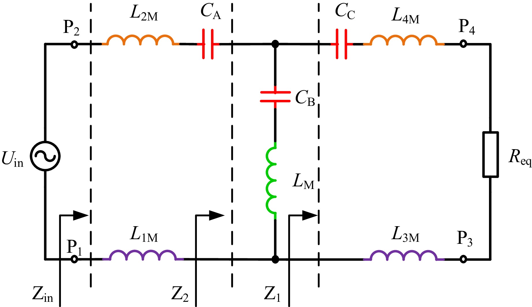
Figure 5.
System T-type decoupled model.
Based on the AC impedance method, the impedances at each stage depicted in Fig. 5 can be expressed as:
$ \begin{split}{Z}_{1}&=\dfrac{1}{\text{j}\omega {C}_{\text{c}}}+\text{j}\omega ({L}_{\mathbf{4M}}+{L}_{\mathbf{3M}})+{R}_{\text{eq}}\\ {Z}_{2}&=\dfrac{{Z}_{1}\cdot \left(\dfrac{1}{\text{j}\omega {C}_{\text{B}}}+\text{j}\omega {L}_{\mathbf{M}}\right)}{{Z}_{1}+\dfrac{1}{\text{j}\omega {C}_{\text{B}}}+\text{j}\omega {L}_{\mathbf{M}}}\\ {Z}_{\text{in}}&={Z}_{2}+\dfrac{1}{\text{j}\omega {C}_{\text{A}}}+\text{j}\omega ({L}_{\mathbf{2M}}+{L}_{\text{1}\mathbf{M}}) \end{split} $ (9) For practical implementations, the electromagnetic coupler is often deliberately designed to be symmetric, specifically featuring identical dimensions between pole pairs P1 and P3, or alternatively, P2 and P4. Furthermore, the distance between P1 and P2 is equal to the distance between P3 and P4. Therefore, the circuit parameters in Fig. 1b have the following relationship:
$ \begin{cases} {C}_{12}={C}_{34}\\ {C}_{14}={C}_{23} \end{cases} \begin{cases} {L}_{1}={L}_{3}\\ {L}_{2}={L}_{4} \end{cases} \begin{cases} {M}_{12}={M}_{34}\\ {M}_{14}={M}_{23} \end{cases} $ (10) According to Eqs (1), (3), and (6), the parameter relationships can be simplified as:
$ \begin{cases} {C}_{1}={C}_{2}\\ {C}_{A}={C}_{C}={C}_{1}+2{C}_{\mathbf{M}} \end{cases} \begin{cases} {L}_{\mathbf{1M}}={L}_{\mathbf{3M}}\\ {L}_{\mathbf{2\boldsymbol{M}}}={L}_{\mathbf{4M}} \end{cases} $ (11) According to Eqs (3) and (11), the electric-field coupling coefficient kCPT, and magnetic-field coupling coefficient kIPT shown in Eqs (2) and (8) can be re-expressed as:
$ \begin{cases} {k}_{\text{CPT}}=\dfrac{{\mathrm{C}}_{A}}{{C}_{A}+{C}_{B}}\\ {k}_{\text{IPT}}=\dfrac{{L}_{\mathbf{M}}}{{L}_{\mathbf{M}}+{L}_{\mathbf{M}}+{L}_{\mathbf{2M}}} \end{cases} $ (12) According to Eqs (9), (11), and (12), if the system works in the input ZPA condition, the imaginary part of the system input impedance should be equal to zero, so the parameters must satisfy one of the equations as follows:
$ {\omega }^{2}{C}_{A}{C}_{B}({L}_{\mathbf{1M}}+{L}_{\mathbf{2M}}+{L}_{\mathbf{M}})={C}_{A}+{C}_{B} $ (13) or
$ \dfrac{2{\omega }^{2}{L}_{\mathbf{M}}{C}_{A}{C}_{B}+2{\omega }^{2}{C}_{A}({L}_{\text{1}\mathbf{M}}+{L}_{\text{2}\mathbf{M}})({C}_{A}+{C}_{B})}{2{\omega }^{4}C_{A}^{2}{C}_{B}({L}_{\text{1}\mathbf{M}}+{L}_{\text{2}\mathbf{M}})({L}_{\text{1}\mathbf{M}}+{L}_{\text{2}\mathbf{M}}+2{L}_{\mathbf{M}})+{\omega }^{2}C_{A}^{2}{C}_{B}R_{\text{eq}}^{2}+2{C}_{A}+{C}_{B}}=1 $ (14) Considering the above two conditions, some system parameters can be solved, as shown in Table 1,where A, B, and C are expressed as follows:
Table 1. System parameters in two ZPA conditions.
System
parametersFirst ZPA condition Second ZPA condition Operating angular frequency $ \omega \text{=}\sqrt{\dfrac{{C}_{\text{A}}\text{+}{C}_{\text{B}}}{\left({L}_{1\text{M}}\text{+}{L}_{\text{2M}}\text{+}{L}_{\text{M}}\right){C}_{\text{A}}{C}_{\text{B}}}} $ $ \begin{cases} {\omega }_{1}\text{=}\sqrt{\dfrac{-B+\sqrt{{B}^{2}-4AC}}{2A}}\\{\omega }_{2}\text{=}\sqrt{\dfrac{-B-\sqrt{{B}^{2}-4AC}}{2A}}\end{cases} $ Input
impedance$ {Z}_{\text{in}}\text{=}\dfrac{{\left(\left({L}_{1\text{M}}\text{+}{L}_{\text{2M}}\right){C}_{\text{A}}-{L}_{\text{M}}{C}_{\text{B}}\right)}^{2}}{\left({L}_{\text{M}}+{L}_{1\text{M}}\text{+}{L}_{\text{2M}}\right)\left({C}_{\text{A}}+{C}_{\text{B}}\right){C}_{\text{A}}{C}_{\text{B}}{R}_{\text{eq}}} $ $ {R}_{\text{eq}} $ Output
voltage$ {\dot{U}}_{\text{out}}=-j{\dot{U}}_{\text{in}}{R}_{\text{eq}}\dfrac{\sqrt{\left({L}_{\text{M}}+{L}_{1\text{M}}\text{+}{L}_{\text{2M}}\right)\left({C}_{\text{A}}+{C}_{\text{B}}\right){C}_{\text{A}}{C}_{\text{B}}}}{\left({L}_{1\text{M}}\text{+}{L}_{\text{2M}}\right){C}_{\text{A}}-{L}_{\text{M}}{C}_{\text{B}}} $ $ {\dot{U}}_{\text{out}}=-{\dot{U}}_{\text{in}}\cdot \dfrac{{\omega }^{2}{C}_{\text{A}}\left({L}_{1\text{M}}\text{+}{L}_{\text{2M}}\right)-1\text{+}j\omega {C}_{\text{A}}{R}_{\text{eq}}}{{\omega }^{2}{C}_{\text{A}}\left({L}_{1\text{M}}\text{+}{L}_{\text{2M}}\right)-1-j\omega {C}_{\text{A}}{R}_{\text{eq}}} $ Output
current$ {\dot{I}}_{\text{out}}=-j\dfrac{\sqrt{\left({L}_{\text{M}}+{L}_{1\text{M}}\text{+}{L}_{\text{2M}}\right)\left({C}_{\text{A}}+{C}_{\text{B}}\right){C}_{\text{A}}{C}_{\text{B}}}}{\left({L}_{1\text{M}}\text{+}{L}_{\text{2M}}\right){C}_{\text{A}}-{L}_{\text{M}}{C}_{\text{B}}} {\dot{U}}_{\text{in}}$ $ {\dot{I}}_{\text{out}}=-\dfrac{{\dot{U}}_{\text{in}}}{{R}_{\text{eq}}}\dfrac{{\omega }^{2}{C}_{\text{A}}\left({L}_{1\text{M}}\text{+}{L}_{\text{2M}}\right)-1\text{+}j\omega {C}_{\text{A}}{R}_{\text{eq}}}{{\omega }^{2}{C}_{\text{A}}\left({L}_{1\text{M}}\text{+}{L}_{\text{2M}}\right)-1-j\omega {C}_{\text{A}}{R}_{\text{eq}}} $ $ \begin{split}A&=C_{\text{A}}^{2}{C}_{\text{B}}\left({L}_{1\text{M}}+{L}_{\text{2M}}\right)\left({L}_{1\text{M}}+{L}_{\text{2M}}+{L}_{\text{M}}\right)\\ B&=C_{\text{A}}^{2}{C}_{\text{B}}R_{\text{eq}}^{2}-2{C}_{\text{A}}{C}_{\text{B}}{L}_{\text{M}}-2{C}_{\text{A}}\left({L}_{1\text{M}}+{L}_{\text{2M}}\right)\left({C}_{\text{A}}+{C}_{\text{B}}\right)\\ C&=2{C}_{\text{A}}+{C}_{\text{B}} \end{split} $ (15) Since the current Iout is independent of Req under the first ZPA condition, the system operates in a CC output mode. For the second ZPA condition, the numerator and denominator of the output voltage Uout are conjugate complex numbers. The modulus of
$ {\dot{U}}_{{\mathrm{out}}} $ $ \begin{split}\left| {\dot{U}}_{\text{out}}\right| &=\left| {\dot{U}}_{\text{in}}\right| \cdot \dfrac{\left| {\omega }^{2}{C}_{\text{A}}\left({L}_{1\text{M}}\text+{L}_{\text{2M}}\right)-1\text+j\omega {C}_{\text{A}}{R}_{\text{eq}}\right| }{\left| {\omega }^{2}{C}_{\text{A}}\left({L}_{1\text{M}}\text+{L}_{\text{2M}}\right)-1-j\omega {C}_{\text{A}}{R}_{\text{eq}}\right| }\\ & \text=\left| {\dot{U}}_{\text{in}}\right| \cdot \dfrac{\sqrt{{\left({\omega }^{2}{C}_{\text{A}}\left({L}_{1\text{M}}\text+{L}_{\text{2M}}\right)-1\right)}^{2}+{\left(j\omega {C}_{\text{A}}{R}_{\text{eq}}\right)}^{2}}}{\sqrt{{\left({\omega }^{2}{C}_{\text{A}}\left({L}_{1\text{M}}\text+{L}_{\text{2M}}\right)-1\right)}^{2}+{\left(-j\omega {C}_{\text{A}}{R}_{\text{eq}}\right)}^{2}}}\text=\left| {\dot{U}}_{\text{in}}\right| \end{split} $ (16) It means the system works in constant voltage (CV) output mode, while the phase of the output voltage is opposite to the input voltage.
-
Employing finite element analysis (FEA) in ANSYS Maxwell, the characteristics of the coupler were analyzed with various dimensions and its spatial structure optimized to improve system performance, with the planar rectangular spiral electromagnetic pole's top view provided in Fig. 6. The self-inductance of the planar square spiral coil is calculated based on the equation as follows:
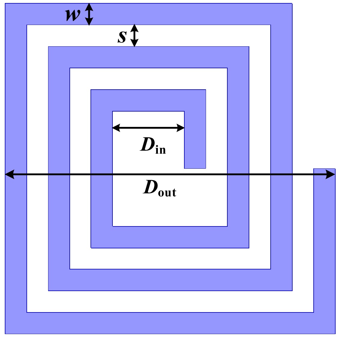
Figure 6.
Top view of the single coil.
$ L=\dfrac{1}{2}{\mu }_{0}{N}^{2}{D}_{\text{avg}}{c}_{1}\left[\ln \left(\dfrac{{c}_{2}}{\rho }\right)+{c}_{3}\rho +{c}_{4}{\rho }^{2}\right] $ (17) where, μ0, N, Davg, and ρ are the vacuum permeability, turns of the coil, average value of inner and outer diameter of the coil
$ ({D}_{\text{avg}}=({D}_{\text{out}}+ {D}_{\text{in}})\text{/2}) $ $ \left(\rho \text{=}\left({D}_{\text{out}}-{D}_{\text{in}}\right)\text{/}\left({D}_{\text{out}}+{D}_{\text{in}}\right)\right) $ In addition, the theoretical formula of a capacitor can be expressed as:
$ C=\dfrac{{\varepsilon }_{0}{\varepsilon }_{r}S}{d} $ (18) where,
$ {\varepsilon }_{\text{0}} $ $ {\varepsilon }_{\text{r}} $ In practice, the outer diameter Dout of the electromagnetic pole is generally determined by the specific application occasion. In this section, the outer electromagnetic pole (P1 and P3) with the size of 500 * 500 mm (Dout = 500 mm) is used for research. According to Eq. (16), when Dout is given, the self-inductance of the outer pole is mainly related to its width of copper foil wout, number of turns Nout, and turns spacing sout. In addition to the aforementioned parameters, the mutual inductances and cross-coupling capacitors are also governed by the width of the copper foil winding of the inner electromagnetic pole, the number of turns Nin, the turn spacing sin, the transmission distance dt, and the inter-pole distance on the same side ds.
Influence of the poles' turns
-
To achieve larger cross-coupling capacitors, Polymethyl methacrylate (PMMA, relative permittivity 3.4) is employed as the dielectric medium separating the electromagnetic poles on each side. The system parameters, as defined in Table 2, are adopted for this investigation.
Table 2. Parameters of the coupler when Nin is variable.
Parameter Value Parameter Value Nout 15 dt 60 mm sout 5 mm sin 5 mm ds 10 mm wout 10 mm win 10 mm Further analysis reveals the changing pattern of input impedance Zin with respect to Nin and Req, as illustrated in Fig. 7[22]. It can be observed that Zin is primarily determined by Req, but the variation with Nin is relatively small. When Req assumes a small value (10−100 Ω), Zin becomes quite high, leading to a minimal amount of power picked up at the load end. When Req takes on a large value (103−104 Ω), Zin ranges from 10 to 100 Ω; however, under CV operating mode, the current picked up by the load remains quite small.
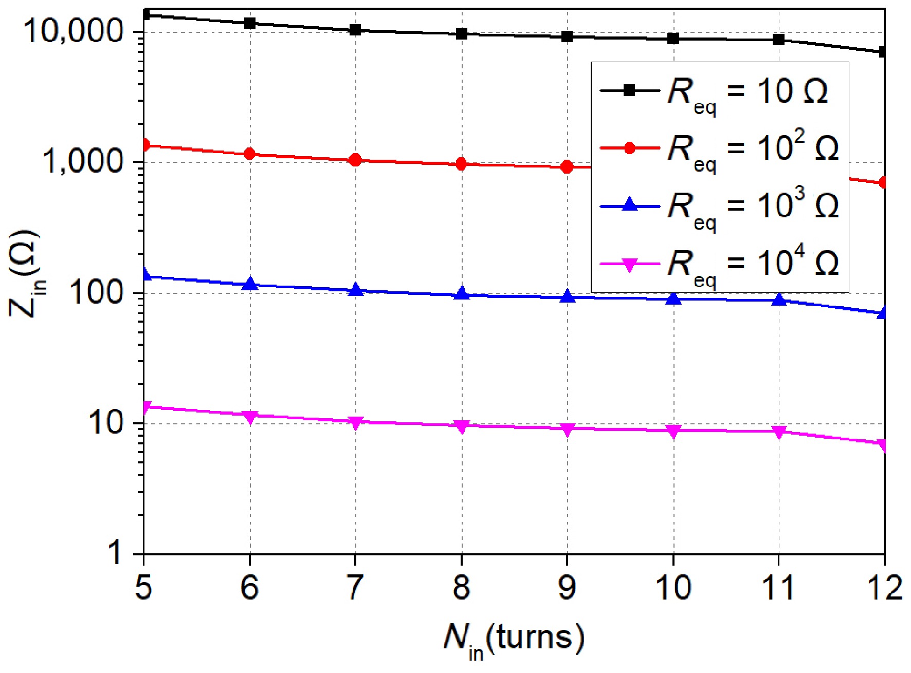
Figure 7.
Variation of the input impedance with Nin and Req[22].
As derived from the preceding analysis, the first ZPA operating mode is exclusively suited for applications characterized by an exceptionally high equivalent load resistance and a minimal load current. Since most practical implementations feature load resistances below 100 Ω, this paper consequently examines the electromagnetic coupler's performance under the second ZPA condition for subsequent analysis and design.
With varying Nin, the self-resonance frequency of the coupler differs significantly, leading to distinct ground voltages of the four electromagnetic poles. The dependence of the ground-referenced voltage at P3 and P4 on Nin is examined under two distinct operating frequencies, f1 and f2, as depicted in Fig. 8[22]. A marked disparity is observed, with UP3 and UP4 demonstrating a substantial increase when the system operates at frequency f2 compared to frequency f1. Therefore, the selection of f1 as the system operating frequency serves to reduce the coupler's fringing electric field and improve overall safety. Subsequent sections are dedicated to the analysis and design of a WPT system targeting operation at the resonant frequency f = f1.
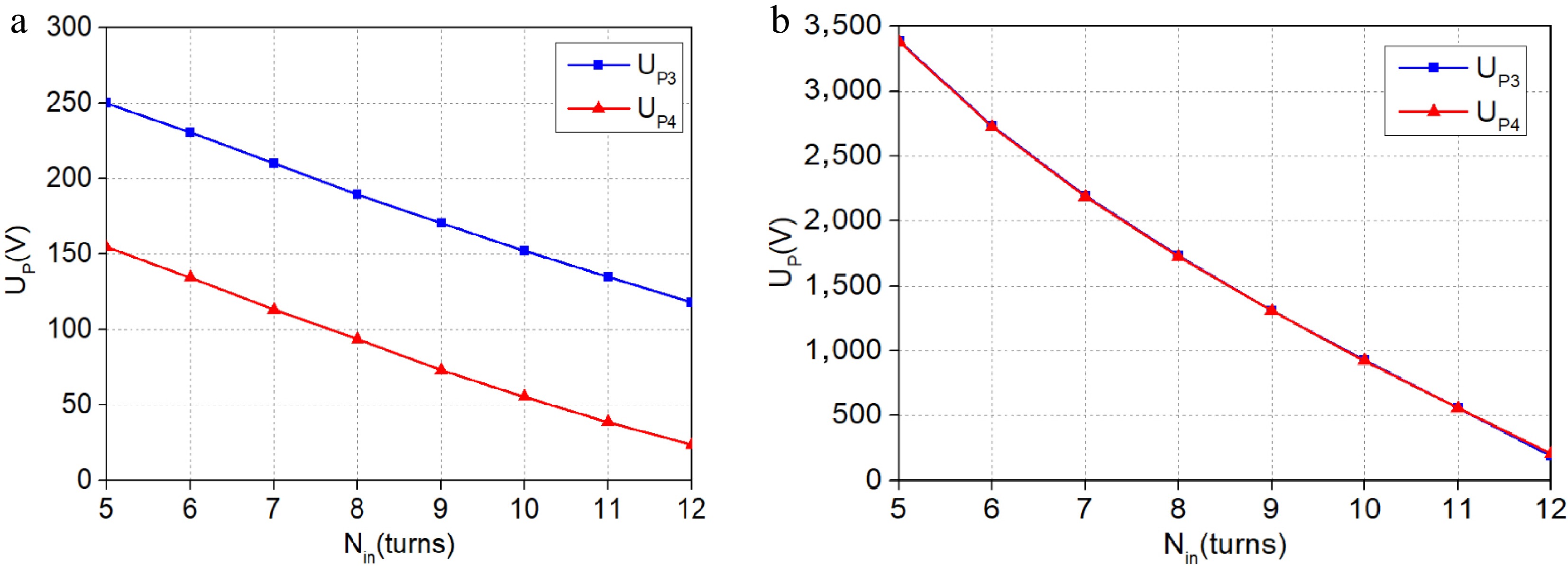
Figure 8.
Ground-referenced voltage curve of P3 and P4[22]. (a) f = f1. (b) f = f2.
Based on the parameters listed in Table 2, the dependence of the self-inductances, mutual inductances, and cross-coupling capacitors of the four electromagnetic poles on Nin can be systematically investigated through Maxwell simulations. Then, the regularity of the magnetic-field coupling coefficient kIPT and electric field coupling coefficient kCPT changing with Nin is obtained as shown in Fig. 9. It can be seen that kIPT is negative, which is related to the setting of the homonymous end of the coupling coil. The determination of the homonymous end is affected by the current direction in the coil, which is related to the winding mode of the coil.
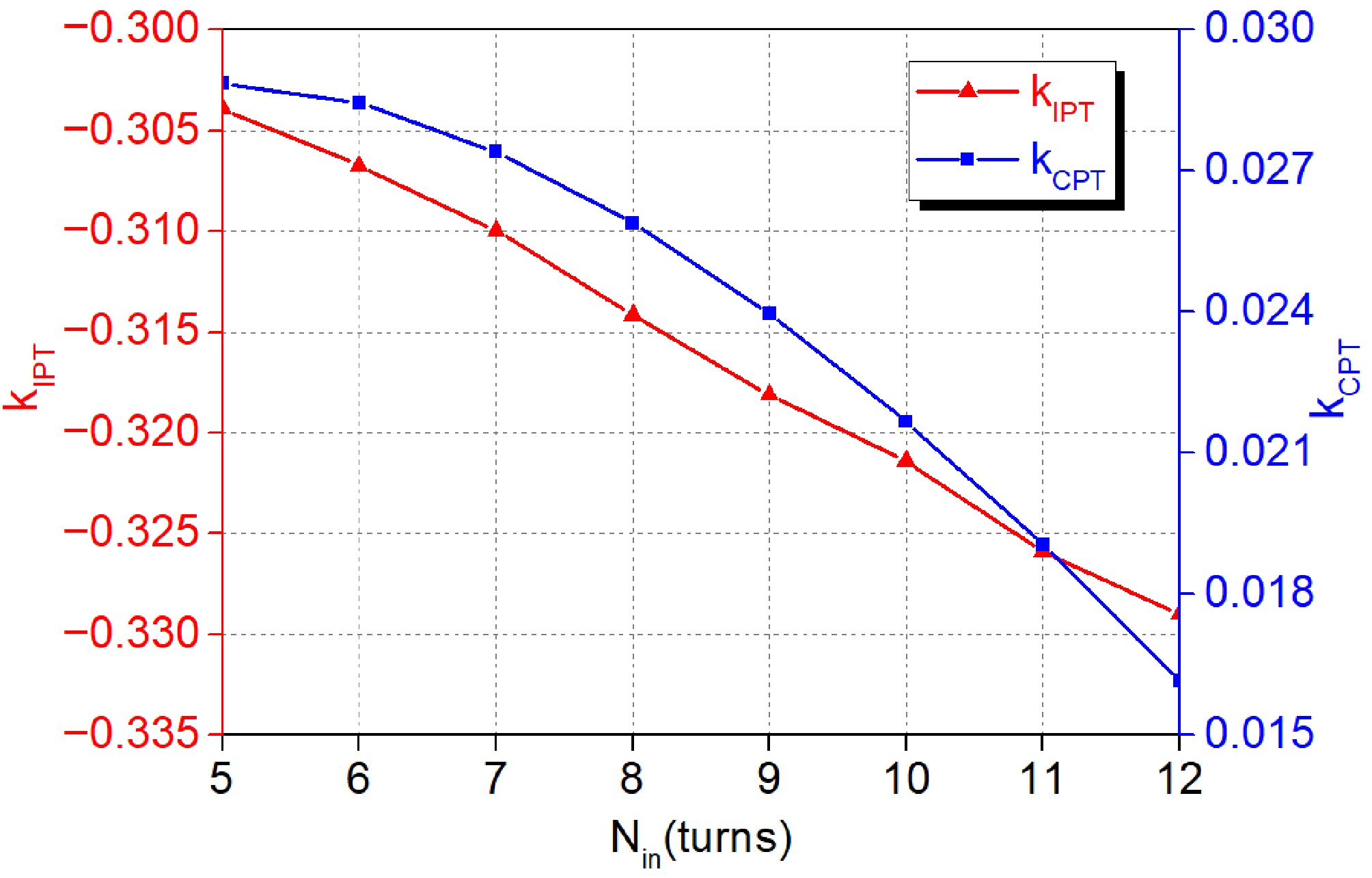
Figure 9.
Variation of magnetic-field and electric-field coupling coefficient.
Influence of the poles' width
-
With the parameters of the coupler listed in Table 3 held constant, the influence of the copper foil width on the system parameters is investigated. In order not to change the occupied area of the outer electromagnetic pole (15 turns, 500 * 500 mm), and the inner electromagnetic pole (nine turns, 330 * 330 mm), the sum of copper foil width and turns spacing in the table is fixed as 15 mm. If the copper foil width changes, the copper-foil turns spacing changes accordingly. Through parametric scanning analysis on Maxwell, The functional dependence of both the magnetic and electric field coupling coefficients on the geometric parameters (copper foil widths win/wout or turn spacings sin/sout) is illustrated in the accompanying contour diagrams, as shown in Fig. 10. A clear correlation is observed whereby the absolute value of kIPT correlates positively with both win and wout, whereas kCPT increases with larger win but decreases with larger wout. Moreover, Fig. 11 shows the regularity of the first resonant frequency f1 varying with win and wout in the case of Req = 40 Ω. It is known that the self-inductances, mutual inductances, and cross-coupling capacitors of the electromagnetic poles increase with the increase of win and wout, so the system resonance frequency decreases, as shown in Fig. 11.
Table 3. Parameters of the coupler when sout and wout are variable.
Parameter Value Parameter Value Nout 15 Nin 9 sout + wout 15 mm dt 60 mm ds 10 mm sin + win 15 mm 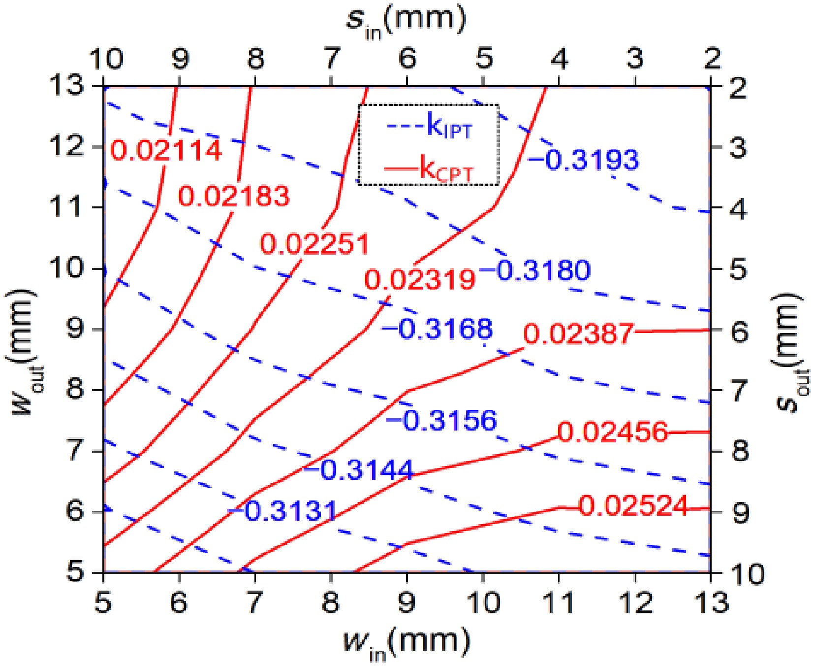
Figure 10.
The variation of coupling coefficient with win and wout (or sin and sout).
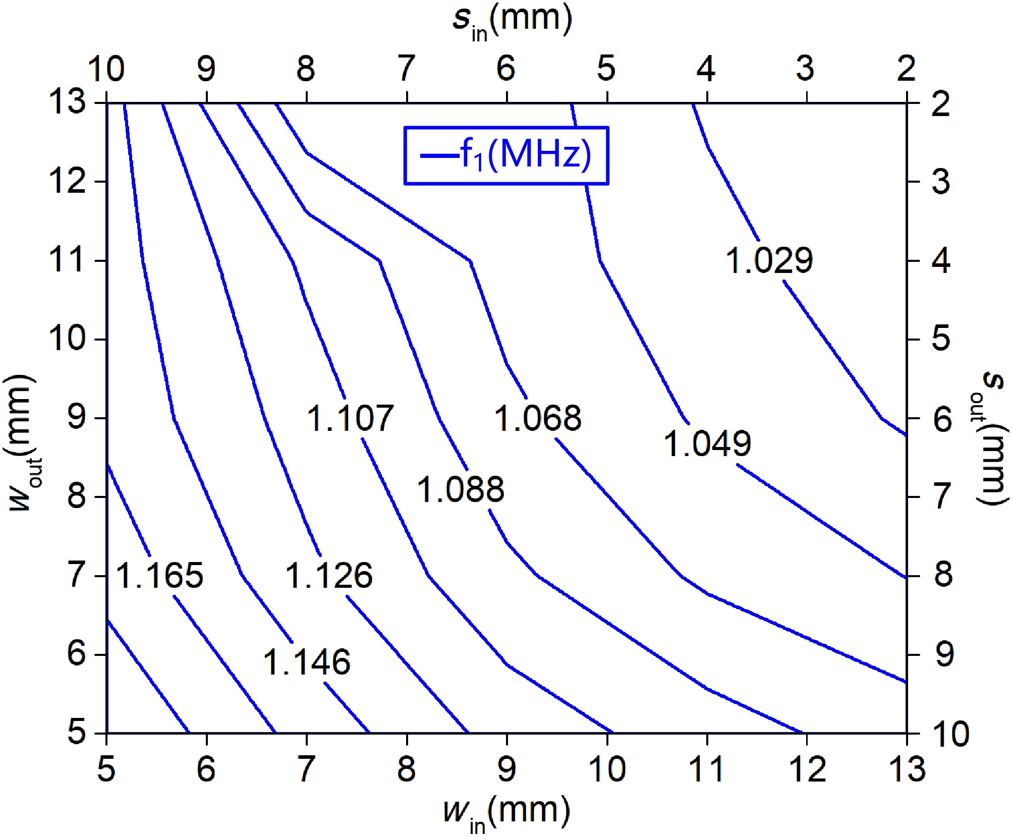
Figure 11.
The variation of the system resonance frequency f1 with win and wout (or sin and sout).
Influence of same-side spacing and transfer distance
-
The transfer distance dt and the same-side electromagnetic poles spacing are set as variables, and the other parameters shown in Table 4 are taken as invariants, then the three-dimensional curved surface of kIPT and kCPT varying with dt and ds can be obtained, as shown in Figs 12 and 13. With the increase of ds, kCPT, and the absolute value of kIPT increase gradually. However, as dt increases, kCPT and the absolute value of kIPT decrease gradually. Generally, the larger the coupling coefficient is, the more conducive to the power transmission. Therefore, it is crucial to carefully balance the relationship between the coupling coefficient and the volume of the coupler when designing the coupler for practical application, which involves selecting appropriate values for ds and dt.
Table 4. Parameters of the coupler when ds and dt are variable.
Parameter Value Parameter Value Nout 15 Nin 9 sout 5 mm sin 5 mm wout 10 mm win 10 mm Req 40 Ω 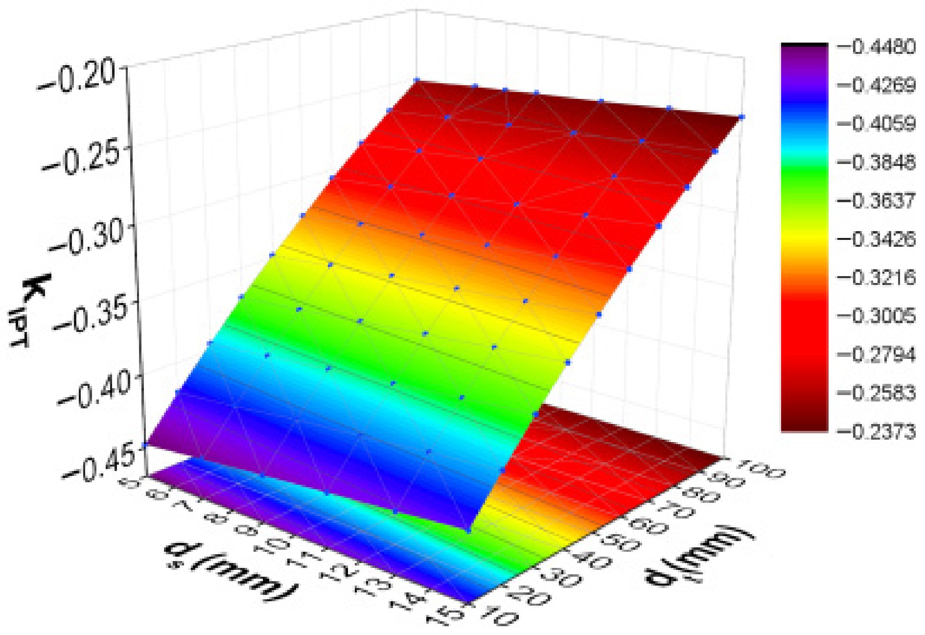
Figure 12.
The variation of kIPT with ds and dt.
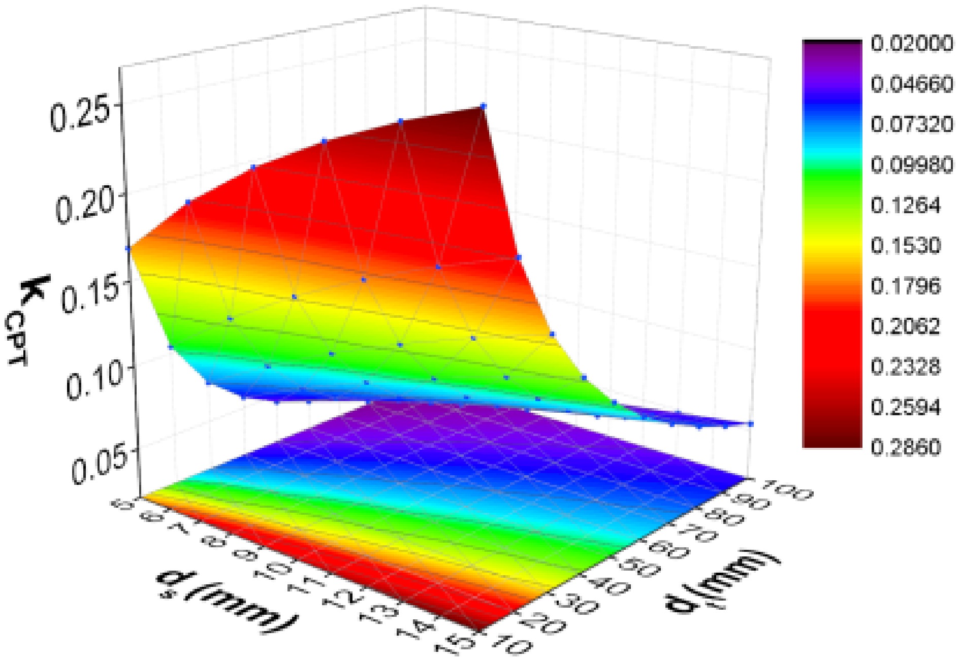
Figure 13.
The variation of kCPT with ds and dt.
Moreover, the changes in self-inductance, mutual inductance, and cross-coupling capacitance with respect to ds and dt can also be obtained, leading to the derivation of the relationship between f1 and ds, as well as dt, as illustrated in Fig. 14. As ds and dt increase, the mutual inductances and cross-coupling capacitances decrease, so the system resonance frequency increases.
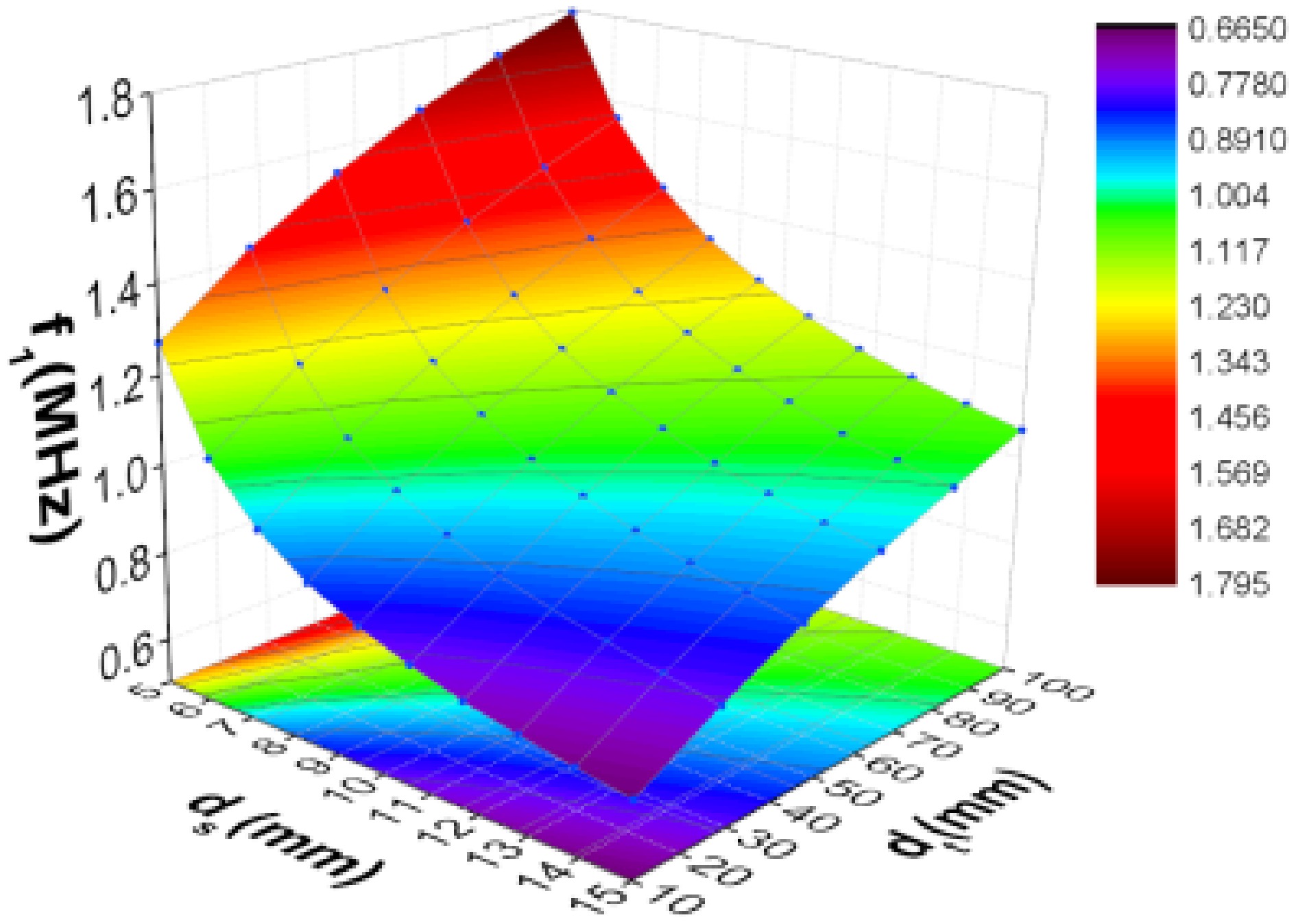
Figure 14.
The variation of f1 with ds and dt.
-
According to the previous literature and experience, the frequency is generally around 1 MHz, so the value of inductance and capacitance will be less affected by the surrounding environment. In addition, the magnetic-field and electric-field coupling coefficient should be balanced, since they determine the system power transmission capability. To systematically optimize the coupler's geometry, the relationship between its parameters and the circuit parameters is investigated. Therefore, the self-inductances, mutual inductances, and cross-coupling capacitors can be obtained by Maxwell. Based on the above analysis in analysis and design of coupler parameters and circuit parameters, if the geometric parameters of the coupler are designed as in Table 5, the operation frequency equals 1.056 MHz, and the magnetic-field and electric-field coupling coefficients are calculated as −0.318 and 0.024, respectively. All the circuit parameters are shown in Table 6. Based on the circuit topology in Fig. 2, and the parameters in Table 6, the system simulation is conducted on MATLAB/Simulink.
Table 5. Geometric parameters of the coupler.
Parameter Value Parameter Value Nout 15 Nin 9 sout 5 mm sin 5 mm wout 10 mm win 10 mm ds 10 mm dt 60 mm Table 6. Circuit parameters for simulation.
Parameter Value Parameter Value Parameter Value f 1.056 MHz M12 22.731μH C12 324.98 pF Udc (Uin) 78.54V
(100 V)M13 28.369 μH C13 30.376 pF RL (Req) 49.348 Ω
(40 Ω)M14 12.367 μH C14 3.0998 pF L1 64.622 μH M23 12.366 μH C23 3.1395 pF L2 19.517 μH M24 7.2848 μH C24 13.198 pF L3 64.407 μH M34 22.722 μH C34 324.14 pF L4 19.432 μH The phase synchronization observed between the inverter output voltage and current in Fig. 15 confirms that the system achieves a unity input power factor by satisfying the ZPA condition. A measured input current amplitude of 2.484 A for the system compares well to the calculated value of 2.5 A. With a variable AC load, the system output voltage is presented in Fig. 16, which shows an acceptable constant voltage output. When the AC load Req increases by 100% (from 40 to 80 Ω), the output voltage increases by 0.4%. When Req decreases by 100% (from 40 to 20 Ω), the output voltage decreases by 1.36%. Table 7 shows the simulation voltages to ground of P1−P4 and the currents through them. P1 and P2 are directly connected with the output port of the inverter, so their amplitude values of the voltage to ground are equal to the inverter output voltage. The currents through P1 and P2 are equal, as well as the currents through P3 and P4, which can be also deduced from the structure shown in Fig. 2. According to IEEE human safety standard[25], the permissible levels for human exposure to electric and magnetic fields are defined by the operating frequency fs in the following manner:
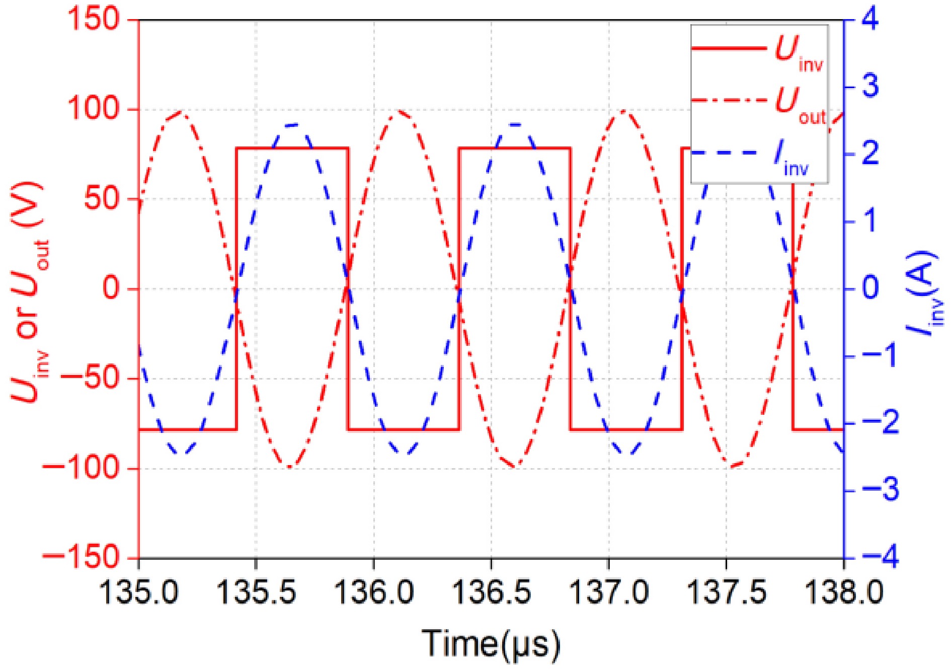
Figure 15.
Simulation waveforms of inverter output voltage and current.
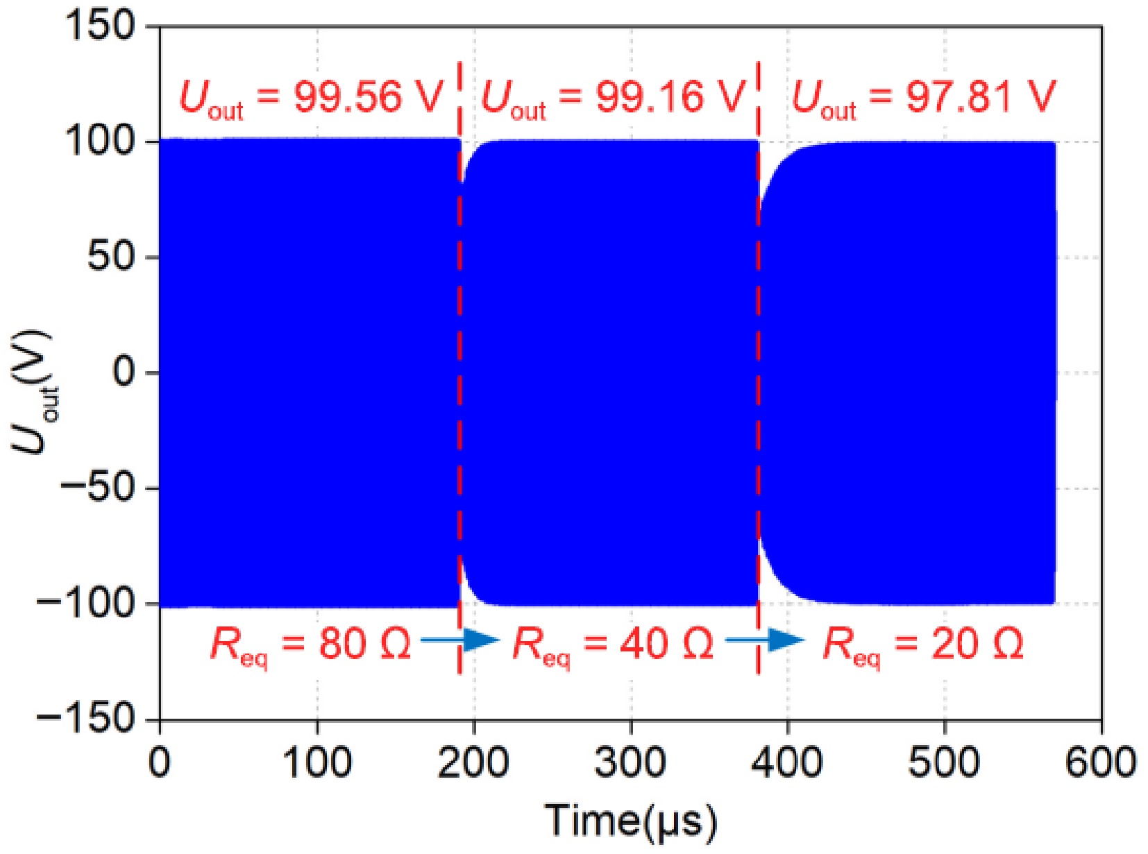
Figure 16.
Simulation waveforms of system output voltage varying with Req.
Table 7. Amplitude value of the voltage to ground and current of P1−P4.
Parameter Value Parameter Value UP1-G 100 V UP2-G 100 V UP3-G 170.9 V UP4-G 72.24 V IP1 2.484 A IP2 2.484 A IP3 2.475 A IP4 2.475 A $ \begin{split} &{E}_{\text{RMS}}=\begin{cases} 614, & 0.1\;\text{MHz}\leq {f}_{s} \lt 1.34\;\text{MHz}\\ 823.8/{f}_{s}, & 1.34\;\text{MHz}\leq {f}_{s} \lt 30\;\text{MHz} \end{cases} \\ &{H}_{\text{RMS}}=16.3/{f}_{s}, 0.1\;\text{MHz}\leq {f}_{s} \lt 30\;\text{MHz} \end{split} $ (19) where, ERMS (V/m) and HRMS (A/m) are the root mean square of the electric field strength and magnetic field strength, respectively. Taking the voltages and currents in Table 7 as the excitation sources, finite element analysis is conducted on ANSYS Maxwell, and the electric field and magnetic field around the coupler are obtained, as shown in Fig. 17a and b, where the safety distance is presented.
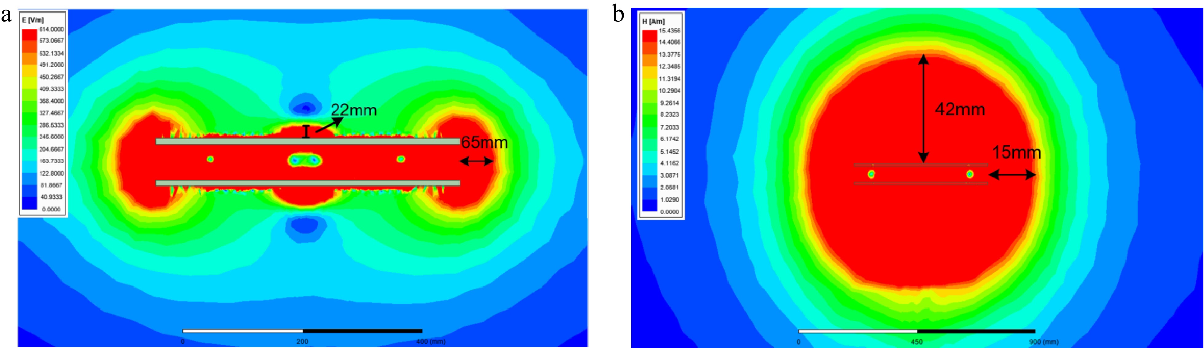
Figure 17.
(a) Electric field distribution around the coupler. (b) Magnetic field distribution around the coupler.
Experimental results
-
Based on the WPT system in Fig. 2 and its equivalent circuit in Figs 3 and 5, the experimental prototype is built with the coupler's dimension parameters in Table 5, as shown in Fig. 18. The coupler is made up of four square planar spiral copper-foil coils (P1−P4) arranged vertically. The copper foil strip is spirally wounded on the surface of acrylic plates. To reduce losses caused by skin effect, we should choose the copper foil with a suitable thickness. So the skin depth of the copper foil should be calculated, which can be expressed as:
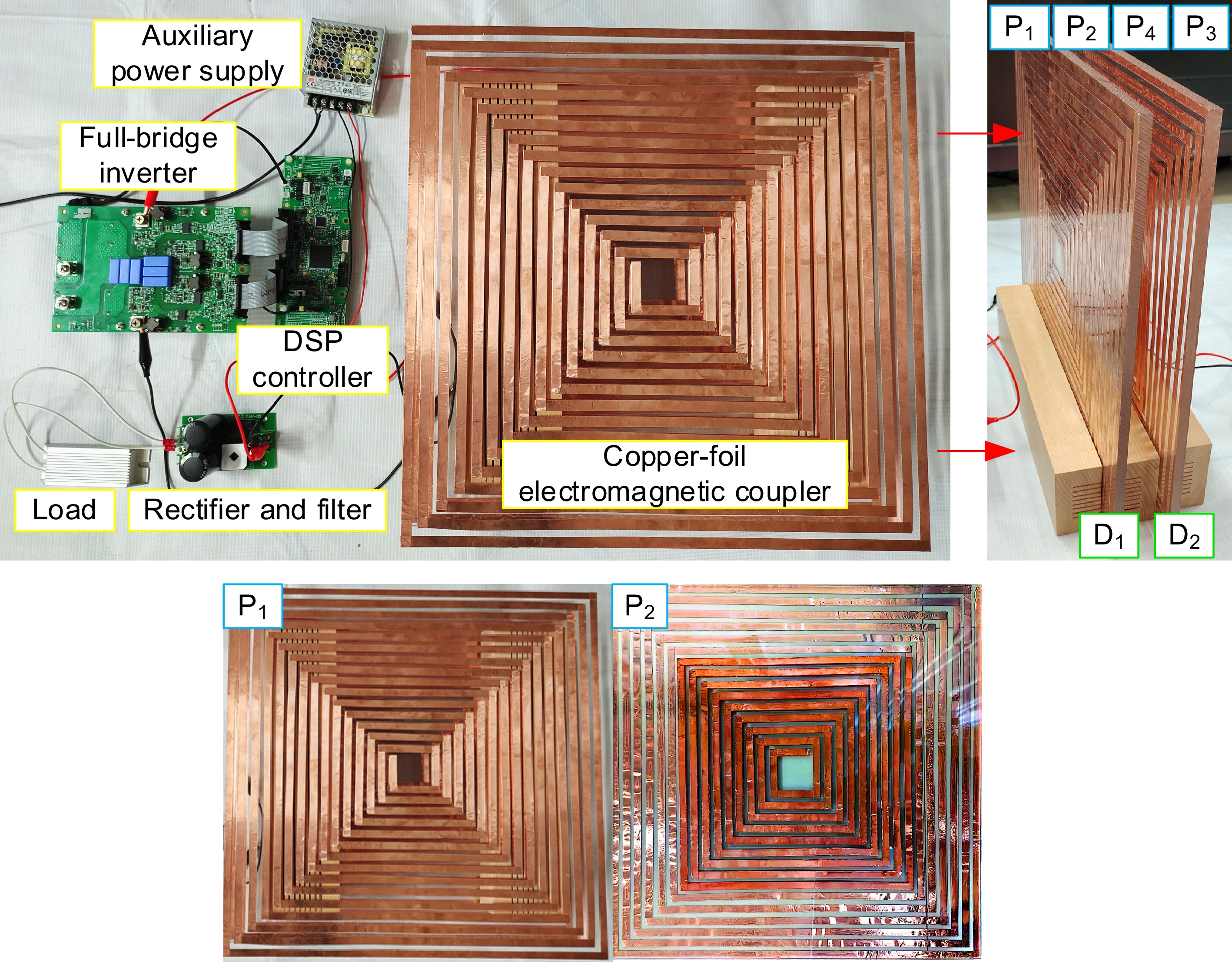
Figure 18.
Experimental prototype of the WPT system.
$ \delta =\sqrt{\dfrac{1}{\pi \mu \sigma f}} $ (20) where, μ is the copper magnetic permeability and equals 4π × 10−7 H/m; σ is the copper conductivity and equals 5.8 × 10⁷ S/m; f is the operating frequency, and the unit is Hz. When f = 1.056 MHz, δ = 64.3 μm, so the copper-foil thickness is approximately selected as 2δ for the experiment. The power transmitter is formed by P1 and P2 attached to D1, while the power receiver is formed by P3 and P4 attached to D2. The self-inductances, mutual inductances, and cross-coupling capacitors are measured using an Agilent E4980A LCR meter, with the results being closely aligned with the simulations in Table 6. The inverter incorporated Cree C2M0080120D SiC MOSFETs, with a TMS320F28335 DSP serving as the digital controller.
The experimental waveforms of the inverter output voltage, current, and AC load voltage are shown in Fig. 19 when the equivalent AC load resistance Req equals 40 Ω. The phase of the inverter output current Iinv lags the inverter output voltage Uinv slightly, which means the input impedance is weakly inductive and zero voltage switching (ZVS) condition is achieved. The phase difference between the inverter output voltage and current is defined as[16]:
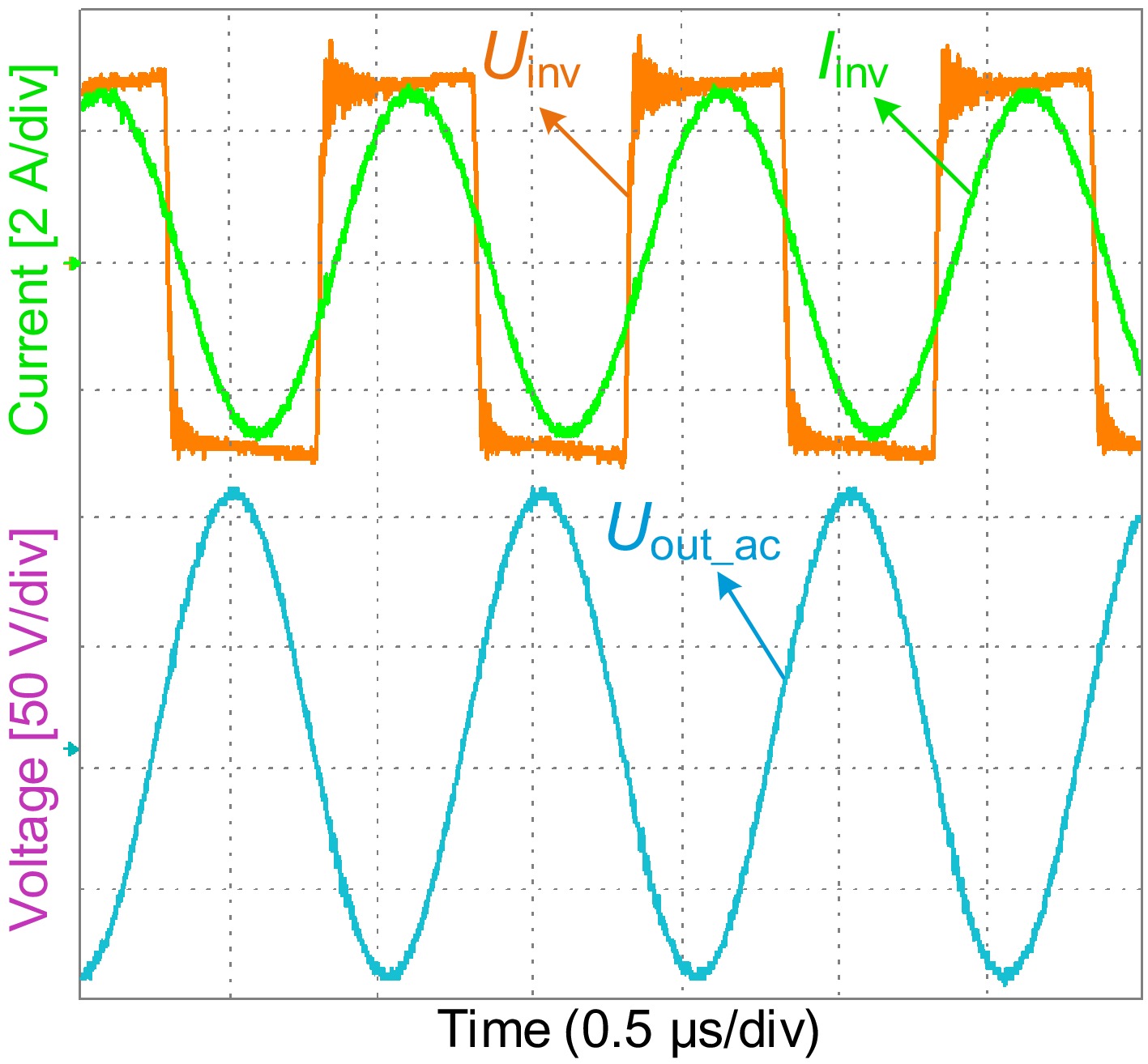
Figure 19.
Experimental waveforms of the inverter output and the AC load voltage.
$ |\theta |\geq \arcsin \dfrac{2{C}_{\text{oss}}{U}_{\text{in}}}{{I}_{\text{in}}{t}_{D}} $ (21) where, Coss and tD represent the parasitic output capacitance and the switching dead time, respectively. It is critical that is fully discharged prior to the transistor turn-on. Furthermore, the inverter output voltage and the AC load voltage are 180° out of phase, while the fundamental component of Uinv is equal to Uout_ac, thereby validating the simulation results presented in Fig. 15. Figure 20 shows the experimental waveforms of the DC load voltage Uout_dc when RL changes from 100 to 50 Ω, then to 25 Ω. With RL increasing or decreasing 100%, Uout_dc changes within 2%, achieving an approximately constant voltage output under a wide load range. The experiment data are measured by a power analyzer when RL equals 50 Ω, as shown in Fig. 21. The input power and output power are 123.83 and 111.84 W, respectively, so the system efficiency is 90.32%. The loss distributions of the experimental prototype are shown in Fig. 22. It can be seen that the system losses are dominated by the four copper-foil electromagnetic poles.
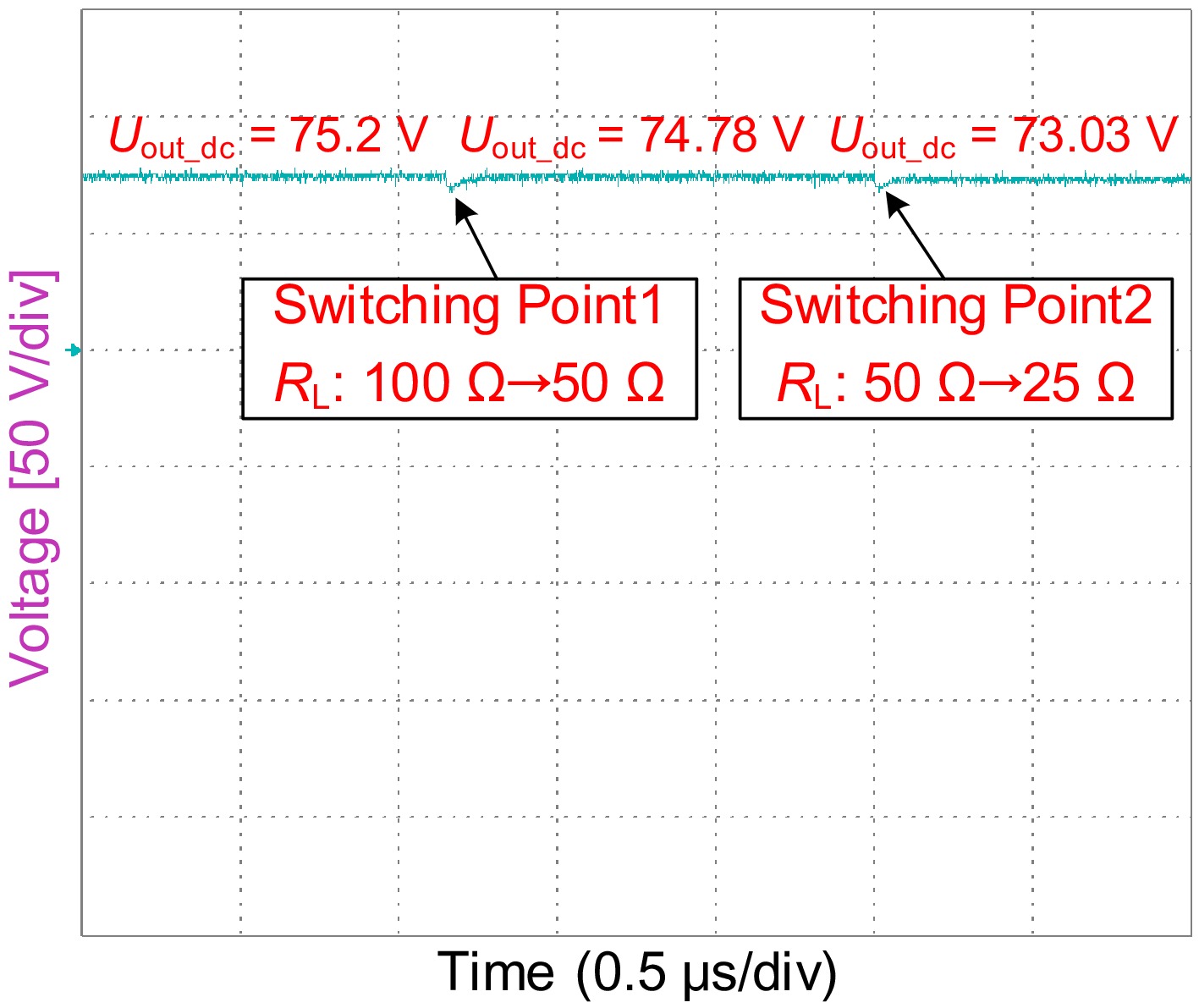
Figure 20.
Experimental waveforms of the DC load voltage when RL changes (100→50→25 Ω).
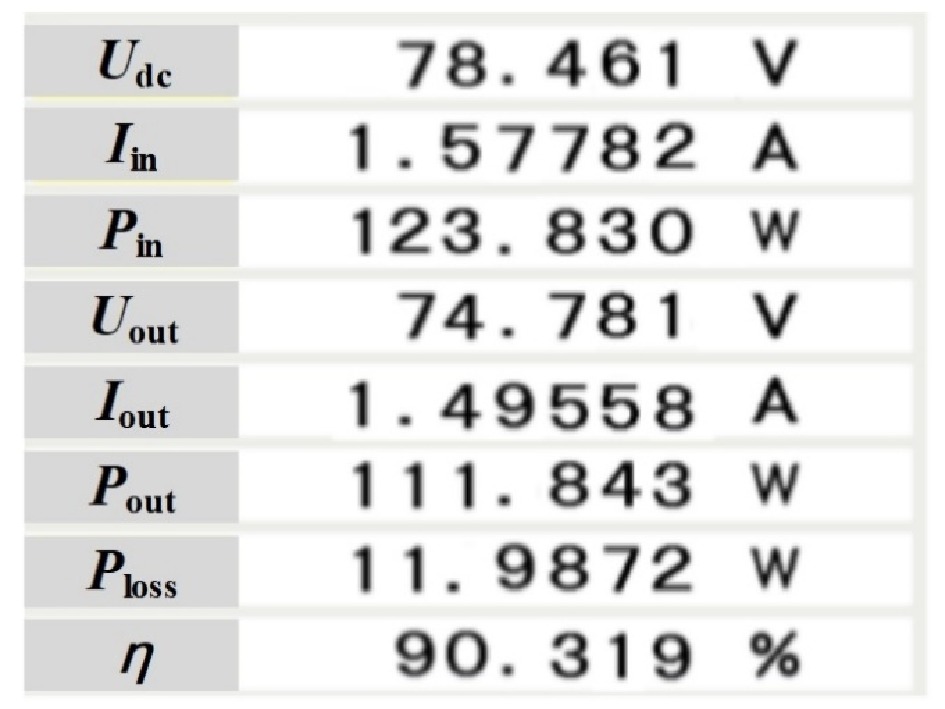
Figure 21.
The experiment results shown in power analyzer.
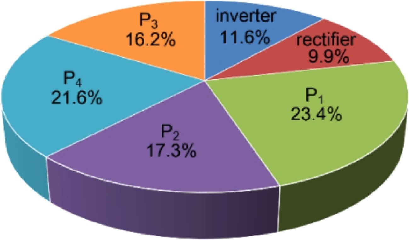
Figure 22.
Loss distributions of the experimental prototype.
The misalignment tolerance of the system was evaluated, and the corresponding results are presented in Fig. 23. It can be seen from the overall trend of change that the output power drops with the X or Y misalignment increasing. The system performance degrades significantly at a misalignment of 150 mm, with both output power and efficiency plummeting to around 30% of those achieved in the perfectly aligned state. When the misalignment increases to about 250 mm, the output power and efficiency are very low. But they rise slightly when the misalignment continues to increase. That's because, the coupling coefficients kCPT and |kIPT| are very small when the misalignment is in the range of (250, 300 mm), and only a little electric power can be transmitted. With the continuous increase of the misalignment, kCPT and |kIPT| return to increase slightly, but both of them are going to end up near zero.
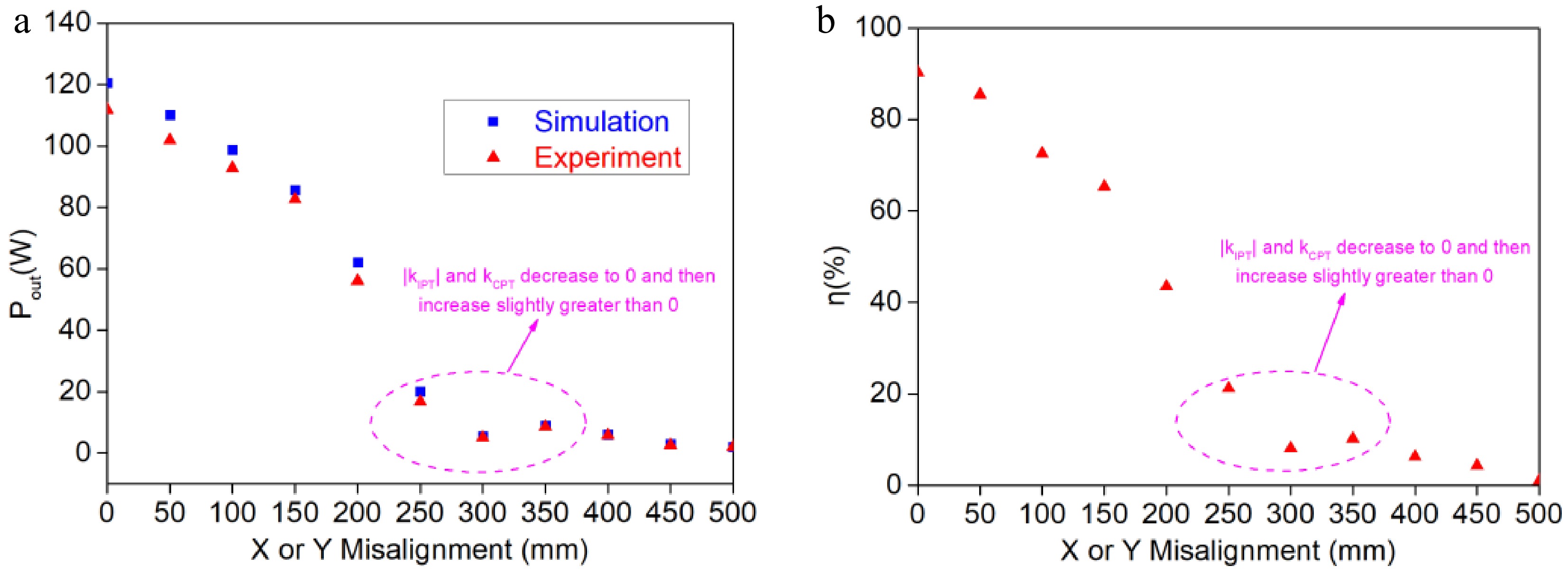
Figure 23.
(a) Test output power of the misalignment ability for this WPT system. (b) Experimental efficiency of the misalignment ability for this WPT system.
-
A copper-foil electromagnetic coupler characterized by the integration of inductance and capacitance, which yields self-resonance, is proposed in this work. The absence of an additional compensation circuit in the proposed hybrid WPT system yields significant benefits, including reduced cost, lighter weight, and structural simplicity. The absence of additional compensation components and the mitigation of the skin effect collectively enhance the overall system efficiency. The relationship between the coupler's geometric parameters and system electrical parameters is analyzed and designed. A wide range of constant voltage output, high power factor, and ZVS conditions are achieved. An experimental device is set up with an output power of 111.84 W and an efficiency of 90.32%.
In addition, the misalignment ability of the prototype should be strengthened in the future. Because the resonant frequency is closely related to the geometric parameters of the coupler, some communication technology and control methods will be applied to this system to improve the misalignment ability. The proposed coupler and system can be well extended to the field of electric vehicles' wireless charging.
-
The authors confirm contribution to the paper as follows: study conception and design: Wu X, Li H; data collection: Wang H, Qing X; analysis and interpretation of results: Lu Z, Wang H, Feng Q; draft manuscript preparation: Wu X, Lu Z. All authors reviewed the results and approved the final version of the manuscript.
-
The datasets generated during and/or analyzed in the current study are available from the corresponding author on reasonable request.
-
This work was supported in part by the research funds of the National Natural Science Foundation of China under Grant No. 52407003 and the Projects Supported by Scientific and Technological Research Program of Chongqing Municipal Education Commission (Grant No. KJQN202501540 and KJQN20230152).
-
The authors declare that they have no conflict of interest.
- Copyright: © 2026 by the author(s). Published by Maximum Academic Press, Fayetteville, GA. This article is an open access article distributed under Creative Commons Attribution License (CC BY 4.0), visit https://creativecommons.org/licenses/by/4.0/.
-
About this article
Cite this article
Wu X, Li H, Wang H, Qing X, Feng Q, et al. 2026. Modeling and decoupling analysis for an integrated coupler and its non-compensated wireless power transfer system. Wireless Power Transfer 13: e019 doi: 10.48130/wpt-0026-0007 

Modeling and decoupling analysis for an integrated coupler and its non-compensated wireless power transfer system
- Received: 13 November 2025
- Revised: 08 December 2025
- Accepted: 31 December 2025
- Published online: 02 July 2026
Abstract: A copper-foil electromagnetic coupler and its equivalent decoupled circuit model are developed in this paper to reduce the weight and cost of Wireless Power Transfer (WPT) systems, and improve system efficiency. The coupler consists of four stacked square spiral copper-foil coils, combining inductance and capacitance to enable the WPT system to function without the need for extra compensation components. The decoupled circuit model of the cross-coupling coils is analyzed and transformed equivalently. Through the design of structure and circuit parameters, the coupler achieves self-resonance. Besides, the conditions of both load-independent constant current or constant voltage output and input zero phase angle (ZPA) are given. The regularities of the electromagnetic coupling coefficient and system resonant frequency varying with the geometric parameters are obtained for system design and optimization. An experimental prototype is implemented and characterized. Under the operating conditions of 1.056 MHz and a 60-mm air-gap distance, measured performance yields an output power of 111.84 W, and a DC-DC conversion efficiency of 90.34%.