


-
Wireless power transfer (WPT) enables the transmission of power through electromagnetic coupling between terminal coils. Compared with the traditional wired charging method, the advantages of WPT technology include: safety, convenience, environmental adaptability, and mobility[1,2], and are extensively applied across multiple industrial domains, such as portable electronic equipment, LED lighting, medical, EVs, and underwater[3−7].
In practical applications, to extend battery life, the two-stage charging method combining constant current (CC), and constant voltage (CV) is commonly adopted. According to the charging profile provided[8], as illustrated in Fig. 1, the initial charging stage operates in constant current mode, where the charging current remains fixed while the charging voltage gradually increases. Once the charging voltage reaches a specified threshold, the system transitions to CV mode. During this phase, the charging voltage tends to stabilize. At the same time the charging current progressively diminishes until the charging process is concluded. It is worth noting that the equivalent load resistance of the battery varies during charging, introducing additional complexity into the design of the WPT system.
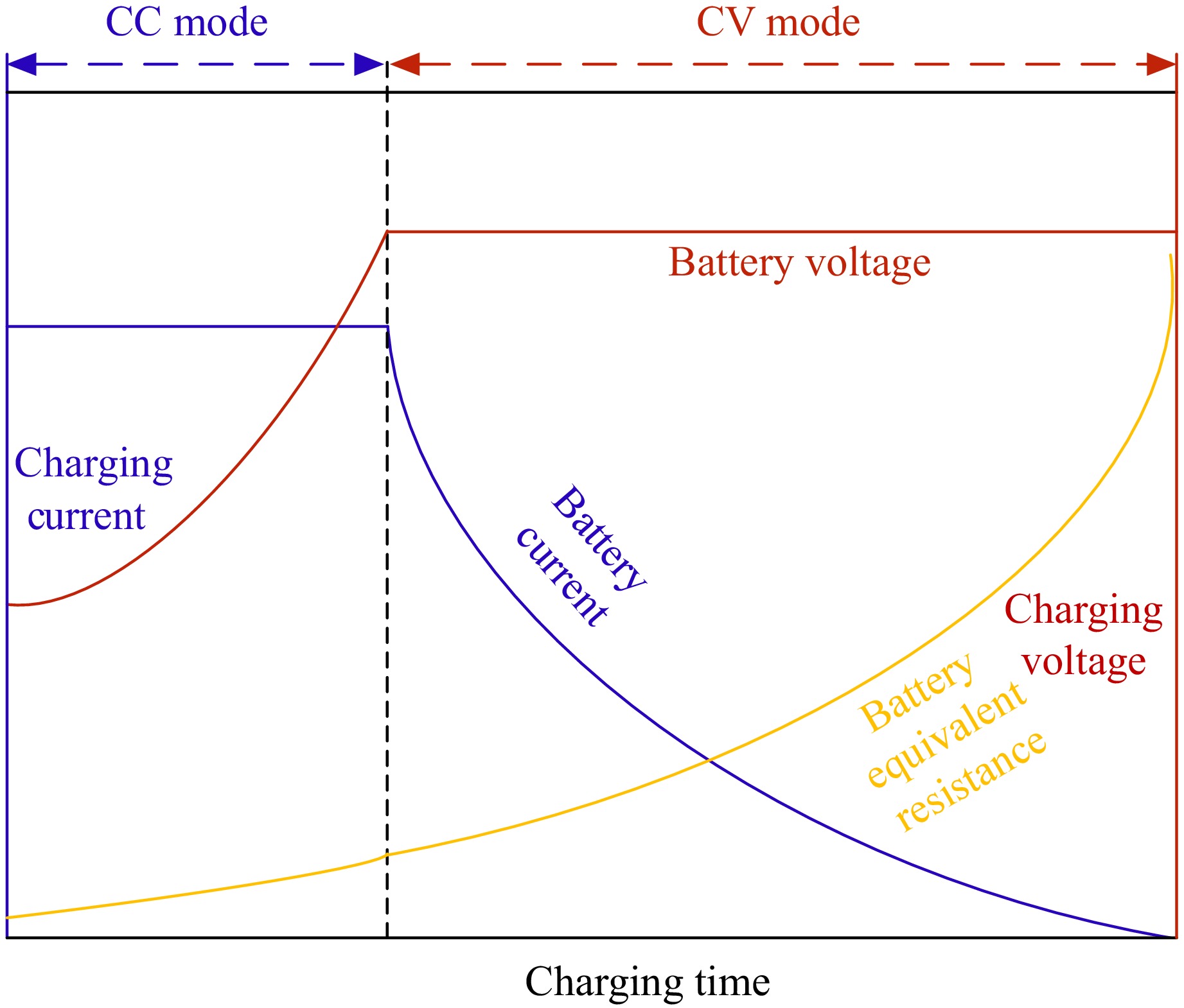
Figure 1.
Charging curve of a battery.
To realize CC and CV output of a WPT system under load variation, researchers have carried out numerous research in recent years. A closed-loop control system based on a DC-DC converter is proposed; however, the introduction of a DC-DC converter increases circuit costs, enhances system complexity, and adds additional losses[9]. A WPT system based on frequency control is presented, but the frequency splitting phenomenon caused by significant frequency changes undermined system stability[10]. A way of switching topologies by switching is proposed, but adds complexity to the circuit[11]. A WPT system that achieves CC and CV output is proposed[12,13], although it utilizes a larger number of compensation components. A multi-coil structure WPT system is presented; however, the mutual inductance between coils significantly affects system output[14,15]. A WPT system with an S/SP compensation structure is proposed; but it still necessitates communication between the primary and secondary sides, although requiring fewer compensation components[16]. A system for isolating a DC-DC converter by an LLC resonant circuit is presented, but it is complex and requires switching[17]. An LCL-S topology without communication is proposed, it increases the complexity of the system by using interference control and PI control on the primary and secondary sides[18]. A WPT system that does not require communication is proposed but still requires switching to reconfigure the circuit structure[19].
Considering the problems of the above WPT system, an S/S compensated WPT system is proposed that enables battery charging in both CC and CV by switching between two specific frequencies, which has a simple structure and uses fewer components to ensure the lightweight and high efficiency of the WPT system[20,21]. In addition, the system employs a method for load estimation and output current estimation and estimates the output voltage based on the estimated load and current. This output voltage will be used as a criterion for the conversion of the operating frequency of the CC to the operating frequency of the CV[22,23].
-
The WPT system architecture with an S/S compensation structure is illustrated in Fig. 2. The system primarily comprises the following components: a DC input power supply Ud; a high-frequency inverter (consisting of four IGBT switches Q1−Q4 for converting DC to AC); transmitting coil inductance Lp and receiving coil inductance Ls; M represents the mutual inductance between the two coils; series capacitors Cp and Cs on the primary and secondary sides; R1 and R2 are the parasitic resistances of the primary and secondary sides, respectively; a rectifier circuit (composed of four MOSFET tubes D1−D4 for converting the received AC to DC for charging); an output filtering capacitor Cf; and RL is the equivalent load resistance of the battery.
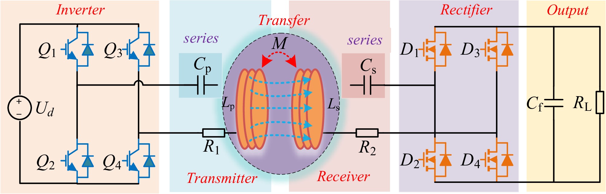
Figure 2.
WPT system architecture with S/S compensation structure.
The voltage output of an inverter circuit is Uin, and the output current is represented by Iin. The current on the primary side is represented by Ip, while the current on the secondary side is represented by Is. The AC equivalent resistance of the rectifier bridge and its subsequent components is represented by Ro, and the current flowing through this resistance is represented by Io. The voltage across this resistance is represented by Uo. Figure 3 provides a detailed illustration of the equivalent circuit of a WPT system employing an S/S compensation strategy.
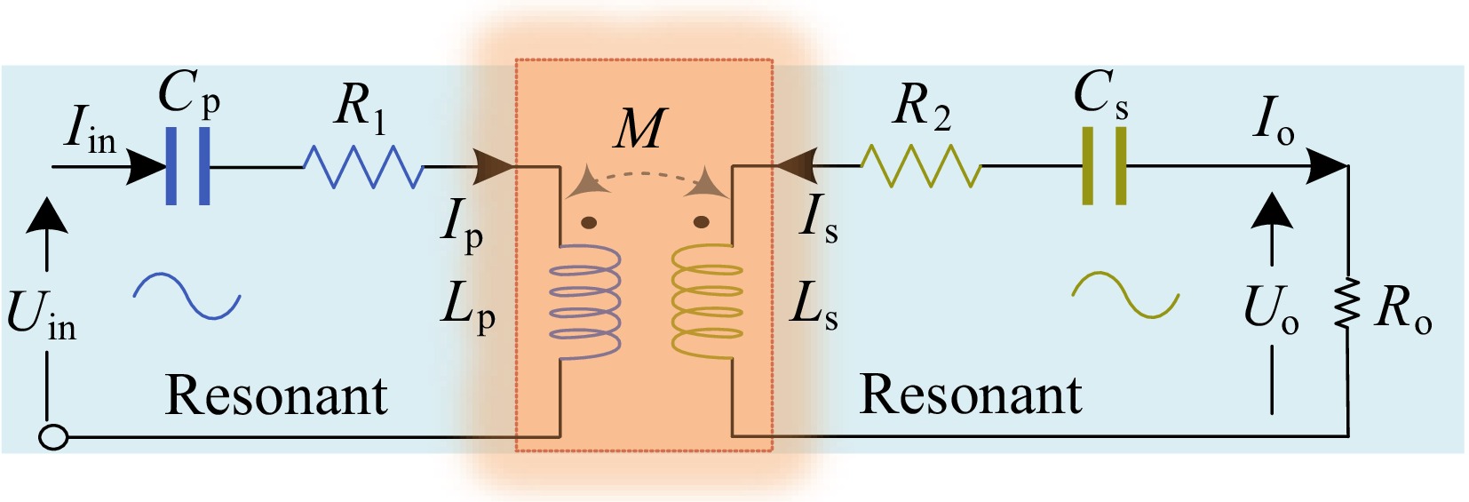
Figure 3.
Equivalent circuit diagram of the WPT system with S/S compensation structure.
Based on the Fundamental Harmonic Approximation (FHA) method, the input voltage Uin can be mathematically represented as follows:
$ {U_{in}} = \dfrac{{2\sqrt 2 }}{\text π}{U_d}\cos \dfrac{\alpha }{2} $ (1) The rectifier bridge and its subsequent AC equivalent resistance Ro is:
$ {R_o} = \dfrac{2}{{{{\text π} ^{}}}}{R_L} $ (2) From the perspective of mutual inductance analysis, the WPT system featuring an S/S compensation structure can be regarded as equivalent to a mutual inductance model, as illustrated in Fig. 4.
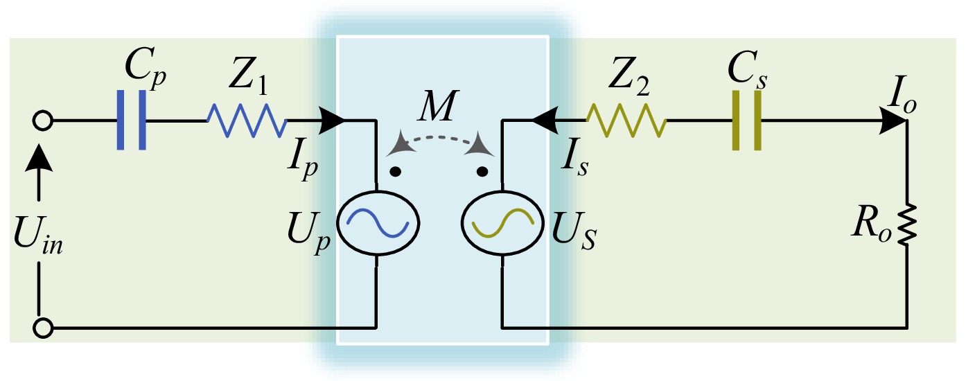
Figure 4.
Mutual inductance model of WPT system with S/S compensation structure.
Where Z1 is the total impedance at the transmitting end, Z2 is the total impedance at the receiving end, and the impedance at the receiving end is equivalent to the impedance at the transmitting end as Zr.
$ \left\{\begin{gathered}Z_1=R_1+\dfrac{1}{\text{j}\omega C_{\text{p}}}+\text{j}\omega L_{\text{p}} \\ Z_2=R_{\mathrm{o}}+R_2+\dfrac{1}{\text{j}\omega C_s}+\text{j}\omega L_s \\ Zr=\dfrac{(\omega M)^2}{Z_2} \\ \end{gathered}\right. $ (3) CC characteristics
-
Using the mutual inductance model, the mutual inductance voltage Us at the receiving end is:
$ U_s=\mathrm{j}\mathit{\omega MI}_p=Z_2I_{s\mathrm{ }} $ (4) Due to the effect of the receiving end, the voltage Up reflected to the transmitting end is:
$ U_p=\mathrm{j}\omega MI_s $ (5) Since the circuit operates in resonance, the total input impedance Zin is:
$ Z_{\text{in}}=Z_1+\dfrac{(\omega M)^2}{Z_2}=R_1+\dfrac{(\omega M)^2}{R_o+R_2} $ (6) The voltage Uin the inverter output can also be expressed in the mutual inductance model as:
$ U_{in}=Z_{\text{l}}I_{\text{p}}+\mathrm{j}\omega MI_{\text{s}}=R_1I_{\text{p}}+\mathrm{j}\omega MI_{\text{s}} $ (7) Since the circuit is in full resonance, the output current amplitude Is and current gain Gi are:
$ I_{\text{s}}=\left|\dfrac{U_{\text{in}}-R_1I\mathrm{_p}}{j\omega M}\right|=\dfrac{U_{\text{in}}-R_1I_{\mathrm{p}}}{\omega M}_{ } $ (8) $ G_i=\left|\dfrac{1}{\mathrm{j}\omega M}\right|=\dfrac{1}{\omega M} $ (9) From Eqns (6), (8) and (9), the S/S topology achieves zero total input impedance Zin at resonance, ensuring that the output current of the system remains load-independent, with a CC gain under varying load conditions.
CV characteristics
-
The current Is at the receiving end passes through the load Ro, and in the resonant state:
$ I_{\text{s}}=\dfrac{U_{\text{s}}}{Z_2}=\dfrac{\mathrm{j}\omega MI_{\text{p}}}{R_{\text{o}}+R_2} $ (10) Then the output voltage at the receiving end is:
$ U_{\mathrm{o}}=I_{\text{s}}R_{\text{o}}=\dfrac{\mathrm{j}\omega MI_{\text{p}}}{R_{\text{o}}+R_2}\cdot R_{\text{o}} $ (11) Since R2 is much smaller than Ro, it will be Ro + R2 ≈ Ro in Eqn (11), so the output voltage at the receiving end will be:
$ U_{\text{o}}=I_{\text{s}}R_{\text{o}}=\dfrac{\mathrm{j}\omega MI_{\text{p}}}{R_{\text{o}}}\cdot R_{\text{o}}=\mathrm{j}\omega MI_{\text{p}} $ (12) Associating Eqns (7) and (12), define the voltage gain as Gv:
$ G\text{v}=\dfrac{U_{\text{o}}}{U_{\text{in}}}=\dfrac{\mathrm{j}\omega MI\mathrm{_p}}{R_1I_{\mathrm{p}}+\mathrm{j}\omega MI_{\text{s}}}_{ } $ (13) From Eqns (12) and (13), the voltage outputted by the system is unaffected by the load, maintaining a consistent voltage gain across varying load conditions. Its total input impedance is the same as in CC mode, and there will be a small impedance angle because the S/S topology cannot achieve full resonance in CV mode.
Load estimation and output current estimation
-
For the WPT system with an S/S structure, a load estimation approach and an output current estimation approach are employed, and the output voltage is estimated based on the estimated load and output current, based on this output voltage, it is used as a criterion for frequency switching from CC to CV. The advantage is that it avoids real-time wireless communication on both sides.
According to Fig. 2, assuming the current flowing through the battery equivalent load RL be IL , in the case of considering only the voltage and current fundamental wave components, the current IL is:
$ I_{L}=\dfrac{1}{\text π} \int_{0}^{\pi} I_{S} \sin (\omega t) d \omega t=\dfrac{2 I_{S}}{\text π} $ (14) The power balance equation, neglecting the power losses in the rectifier during the following derivation is:
$ (I_L)^2R_L=\left(\dfrac{I_S}{\sqrt{2}}\right)^2R\mathrm{_o} $ (15) In the equivalent circuit model shown in Fig. 3, based on Eqns (14) and (15), the current Io flowing through Ro is derived as:
$ {I_{\rm o}} = \dfrac{\text π}{{2\sqrt 2 }}{I_L} $ (16) Applying Kirchhoff's Voltage Law (KVL):
$ \left[\begin{array}{*{20}{c}}Z_1 & \mathrm{j}\omega M \\ \mathrm{j}\omega M & Z_2\end{array}\right]\left[\begin{array}{*{20}{c}}I_p \\ I_s\end{array}\right]=\left[\begin{array}{*{20}{c}}U\mathrm{_{in}} \\ 0\end{array}\right] $ (17) Based on Eqns (3) and (17), the resonant currents at the two coils can be deduced as:
$ \left\{\begin{array}{*{20}{l}}I_p=\dfrac{Z_2}{\left(\omega M\right)^2+Z_1Z_2}\times U_{in} \\ I_s=\dfrac{1}{j}\times\dfrac{\left(\omega M\right)}{\left(\omega M\right)^2+Z_1Z_2}\times U_{in}\end{array}\right. $ (18) Equation (18) demonstrates that changes in RL affect Ip, subsequently altering the active power P1 delivered to the battery, indicating a correlation between RL and P1. By calculating P1, RL can be indirectly estimated. The voltage-current on the battery equivalent load RL can also be derived from the current Ip at the transmitting end through Eqns (2) and (18), it shows that even if we don't know RL, the voltage-current on RL can be regulated by Ip. It is worthy of attention that both Ip and P1 are measurable/computable variables at the transmitter side, which just solves the proposed problem of avoiding bilateral wireless communication.
Firstly, the method for estimating the load output current IL is derived. When the WPT system operates under resonance and the parasitic resistances R1 and R2 are neglected, the RMS value of the emitter current Ip can be determined using Eqns (1), (2), (16), and (18) as:
$ {I_{p{\__{{\text{RMS}}}}}} = \dfrac{{16\sqrt 2 {R_L}}}{{{{\text π} ^3}{{\left( {\omega M} \right)}^2}}}{U_d}\cos \dfrac{\alpha }{2} $ (19) From Eqn (19), the variation of RL affects Ip_RMS, and then the adjustment of the current IL flowing through the battery equivalent load RL by controlling Ip_RMS is analyzed as follows.
$ {I_{p{\__{{\text{RMS}}}}}} = \dfrac{\text π}{{2\sqrt 2 }}\dfrac{{{I_L}}}{{\omega M}}\sqrt {{{\left( {\dfrac{A}{{\omega {C_S}}}} \right)}^2} + {{\left( {{R_2} + \dfrac{8}{{{{\text π} ^2}}}{R_L}} \right)}^2}} $ (20) From this it is then possible to deduce the equation for estimating the load output current IL, where A = 1 − ωLsCs.
Secondly extrapolating the estimation method of load resistance, based on Eqn (20) and assuming that the battery is a resistor, it is apparent from Fig. 3 that the impedance Z1 on the primary side, introduced into the magnetic coupler for S/S compensation, is expressed by the following equation:
$ \begin{split} {Z_1} =\;& \left[ {{R_1} + \dfrac{{{{\left( {\omega M} \right)}^2}{{\left( {\omega {C_s}} \right)}^2}\left( {{R_2} + {R_o}} \right)}}{{{{\left( {\omega {C_s}} \right)}^2}{{\left( {{R_2} + {R_o}} \right)}^2} + {{\left( {1 - {\omega ^2}{L_s}{C_s}} \right)}^2}}}} \right] \\ & + j\left[ {\omega {L_p} + \dfrac{{{{\left( {\omega M} \right)}^2}\left( {\omega {C_s}} \right)\left( {1 - {\omega ^2}{L_s}{C_s}} \right)}}{{{{\left( {\omega {C_s}} \right)}^2}{{\left( {{R_2} + {R_o}} \right)}^2} + {{\left( {1 - {\omega ^2}{L_s}{C_s}} \right)}^2}}}} \right] \end{split} $ (21) Assuming negligible losses on the secondary side, the power delivered to the battery equals power consumption in the actual use of Z1. The active power P1 is thus derived as:
$ {P_1} = I_{p{\__{{\text{RMS}}}}}^2\left[ {{R_1} + \dfrac{{{{\left( {\omega M} \right)}^2}{{\left( {\omega {C_s}} \right)}^2}\left( {{R_2} + {R_o}} \right)}}{{{{\left( {\omega {C_s}} \right)}^2}{{\left( {{R_2} + {R_o}} \right)}^2} + {{\left( {1 - {\omega ^2}{L_s}{C_s}} \right)}^2}}}} \right] $ (22) When the system is operating at resonance, the battery equivalent resistance RL is:
$ {R_L} = \dfrac{{{{\text π} ^2}}}{8}\left[ {\dfrac{{{{\left( {\omega M} \right)}^2}I_{P{\__{{\text{RMS}}}}}^2}}{{{P_1} - {R_1}I_{P{\__{{\text{RMS}}}}}^2}} - {R_2}} \right] $ (23) Calculation of resonant frequency
-
According to Fig. 4, we define I(ω) as the proportion of output current to input voltage:
$ I(\omega)=\dfrac{I_o}{U_{\text{in}}}=\dfrac{\mathrm{j}\omega M}{Z_1Z_2+\omega^2M^2} $ (24) According to Fig. 4, we define E(ω) as the voltage transfer ratio of the output voltage-to-input voltage, which in combination with Eqn (13) yields:
$ E(\omega)=\dfrac{U_o}{U_{\text{in}}}=\dfrac{\mathrm{j}\omega MR\mathrm{_o}}{Z_1Z_2+\omega^2M^2} $ (25) The ωp and ωs represent the primary and secondary resonant angular frequencies of the system.
$ {\omega _P} = \dfrac{1}{{\sqrt {{L_P}{C_P}} }}{\text{ and }}{\omega _S} = \dfrac{1}{{\sqrt {{L_S}{C_S}} }} $ (26) In previous applications, their ratios were:
$ \mu = \dfrac{{{\omega _P}}}{{{\omega _S}}} $ (27) We can derive the characteristics of the ideal transconductance Ii(ω) and the ideal voltage transfer ratio Ei(ω) by assuming R1 = R2 = 0. At specific operating frequencies, the transfer functions Ii and Ei exhibit load-independent properties. To identify these specific operating frequencies, we set the Ro coefficients in Eqns (24) and (25) to zero. The load-independent Gi can be operated at ωp and its magnitude is determined as:
$ |{G_i}({\omega _P})| = \dfrac{1}{{{\omega _P}k\sqrt {{L_P}{L_S}} }} $ (28) Note that in the design, k is the coupling coefficient, and Eqn (27) should be satisfied that μ is close to 1, i.e., ωp ≈ ωs. Similarly, Ei is given by the following equations for a CV output:
$ \left| {{E_i}({\omega _L})} \right| = \sqrt {\dfrac{{{L_S}}}{{{L_P}}}} \left| {\dfrac{{k({\mu ^2} + 1 - {{\Delta }})}}{{(2{k^2} - 1){\mu ^2} + 1 - {{\Delta }}}}} \right| $ (29) $ |{E_i}({\omega _H})| = \sqrt {\dfrac{{{L_S}}}{{{L_P}}}} \left| {\dfrac{{k({\mu ^2} + 1 + {{\Delta }})}}{{(2{k^2} - 1){\mu ^2} + 1 + {{\Delta }}}}} \right| $ (30) Included among these,
$ \Delta = \sqrt {{{(1 - {\mu ^2})}^2} + 4{k^2}{\mu ^2}} $ $ {\omega _L} = {\omega _S}\sqrt {\dfrac{{{\mu ^2} + 1 - {{\Delta }}}}{{2(1 - {k^2})}}} $ (31) $ {\omega _H} = {\omega _S}\sqrt {\dfrac{{{\mu ^2} + 1 + {{\Delta }}}}{{2(1 - {k^2})}}} $ (32) Therefore, the WPT system with S/S structure operates at the frequency calculated by Eqn (26) in CC mode and at the frequency calculated by Eqns (31) and (32) in CV mode.
Based on all the theoretical formulas of the WPT system with S/S structure, a set of achievable parameters of the proposed system is designed as presented in Table 1.
Table 1. Theoretical circuit parameters.
Parameters Value fcc (kHz) 70 fcv (kHz) 91.7 Cp (nF) 18.546 Cs (nF) 18.221 Lp (μH) 280 Ls (μH) 285 M (μH) 115.918 R1 (Ω) 0.15 R2 (Ω) 0.1 -
Based on the theoretical parameters of Table 1 and simulation of Eqns (6) and (8) by MATLAB, the relationship between the load resistance RL and the output current and input impedance angle under different frequencies are plotted as illustrated in Fig. 5.
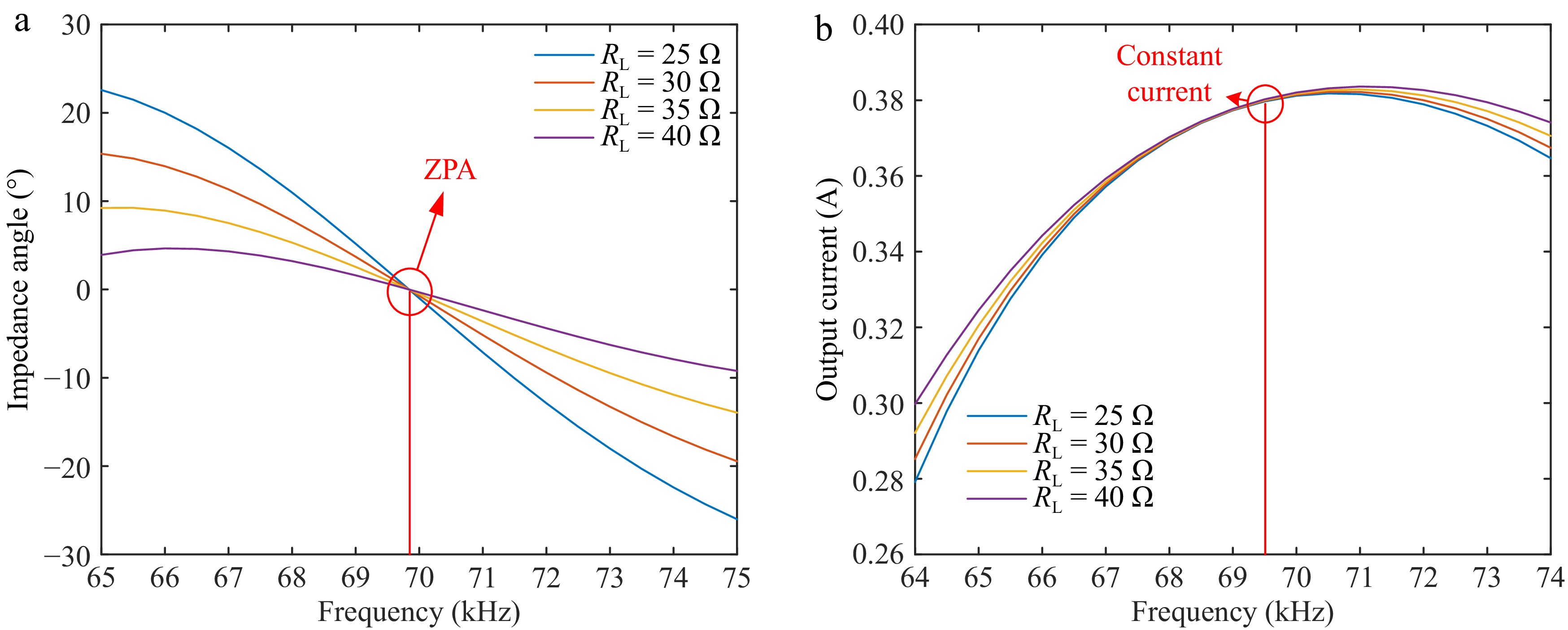
Figure 5.
Relationship between load resistance RL and output current and input impedance angle under different frequencies in CC mode. (a) Impedance angle under different loads for frequency change. (b) CC output characteristics.
In Fig. 5a, it can be seen that when the frequency is close to 70 kHz, the impedance angle is zero under different loads and implemented ZPA feature. In Fig. 5b, it can be seen that when the frequency is close to 70 kHz, the CC output of 0.38 A can be realized, and although the output current can be higher around 71 kHz, the increase is not large enough to be negligible, and the CC characteristic of the system is weakened at 71 kHz. In summary, the CC resonant frequency of the system is selected as 70 kHz.
The relationship between the load resistance RL and the output voltage and input impedance angle at different frequencies by simulating Eqns (6) and (12) in MATLAB are shown in Fig. 6.
From Fig. 6a, it can be seen that the S/S topology has a small impedance angle in CV mode and does not achieve the zero phase angle characteristic. From Fig. 6b, it can be concluded that the S/S topology will achieve a CV output of 23 V at a frequency of about 91.7 kHz.
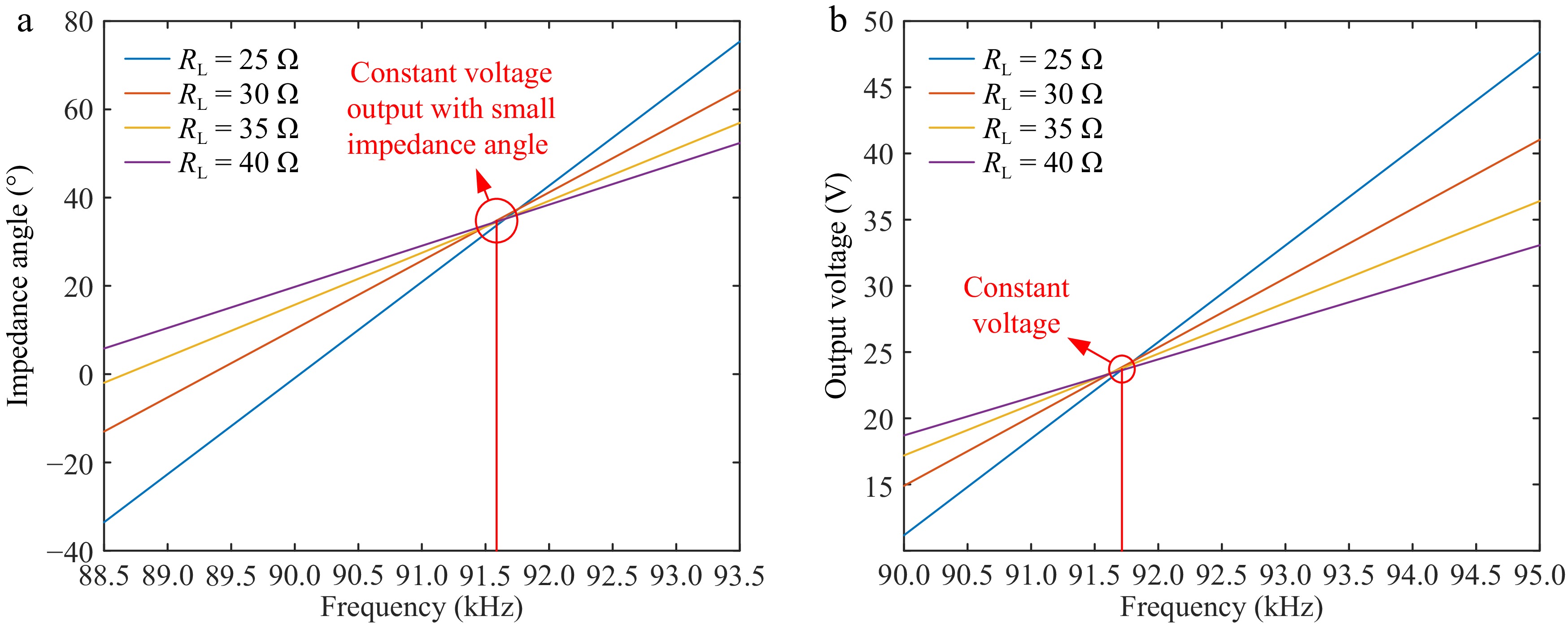
Figure 6.
Relationship between load resistance RL and output voltage and input impedance angle under different frequencies in CV mode. (a) Impedance angle under different loads for frequency change. (b) CV output characteristics.
To verify the feasibility of the proposed WPT system with S/S topology, a set of simulation circuits with 0.38 A/23 V charging output is built in MATLAB/Simulink. The switching strategy of the system is shown in Fig. 7.
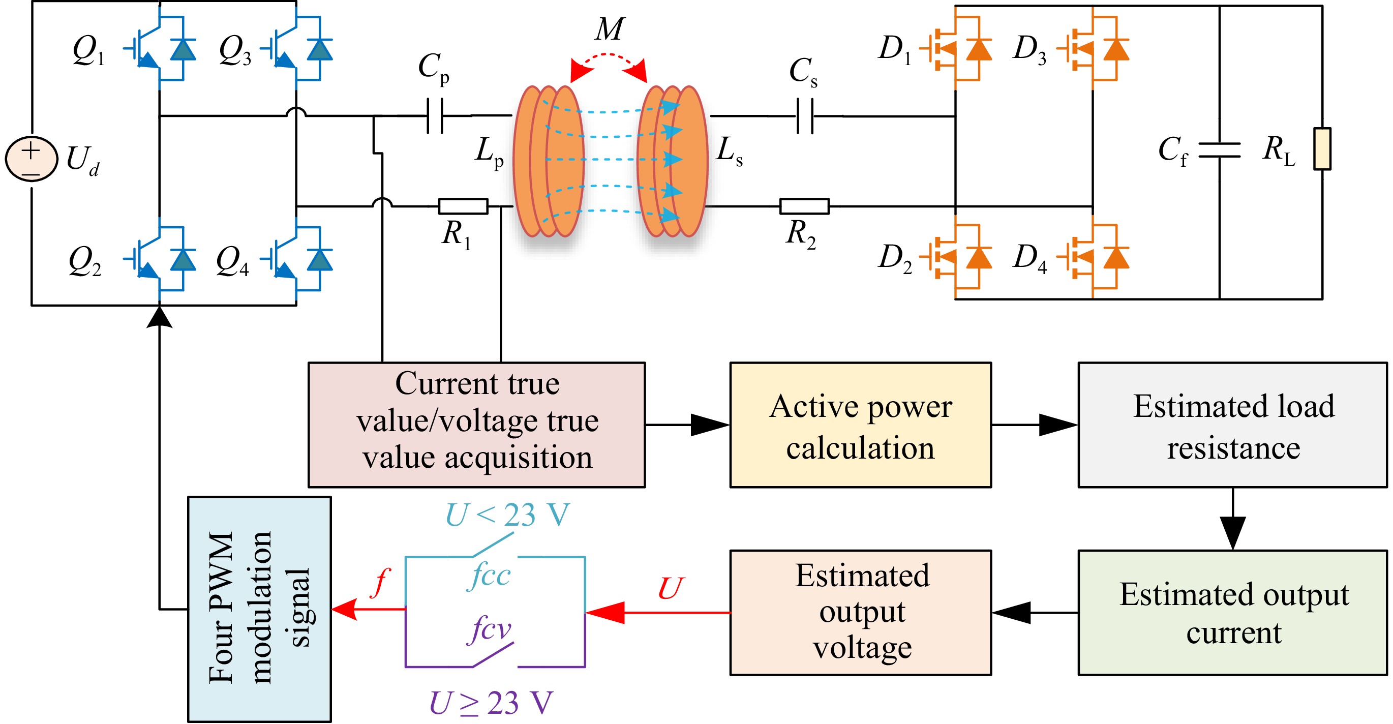
Figure 7.
System switching strategy.
The system operates initially at a CC resonant frequency of 70 kHz, delivering a constant current of 0.38 A to the battery load. This phase ensures a stable charging current, as depicted in Fig. 8. During this stage, the charging process starts with a relatively low load resistance, enabling a consistent current supply to the battery. As the charging progresses, the battery's state of charge (SOC) increases, leading to a gradual rise in the load resistance of the system. Consequently, the voltage across the load terminals also increases proportionally, following Ohm's Law. When the charging voltage at the load terminals reaches 23 V, this marks the transition point where the system needs to switch from CC mode to CV mode to ensure safe and efficient charging. At this transition point, the controller on the transmitter side dynamically adjusts the operating frequency of the system from the CC resonant frequency of 70 kHz to the CV resonant frequency of 91.7 kHz. This frequency shift ensures that the system can maintain a stable voltage of 23 V across the load terminals, as illustrated in Fig. 9. During the CV charging phase, the charging voltage remains fixed at 23 V, while the charging current gradually decreases. This decrease is a natural result of the increasing load resistance as the battery approaches full charge. The current continues to decline until it reaches a predefined cutoff threshold, signaling the end of the charging process. This seamless frequency switching between the CC and CV modes, coupled with dynamic voltage and current control, ensures efficient and safe battery charging while protecting the system components from overvoltage or overcurrent conditions.
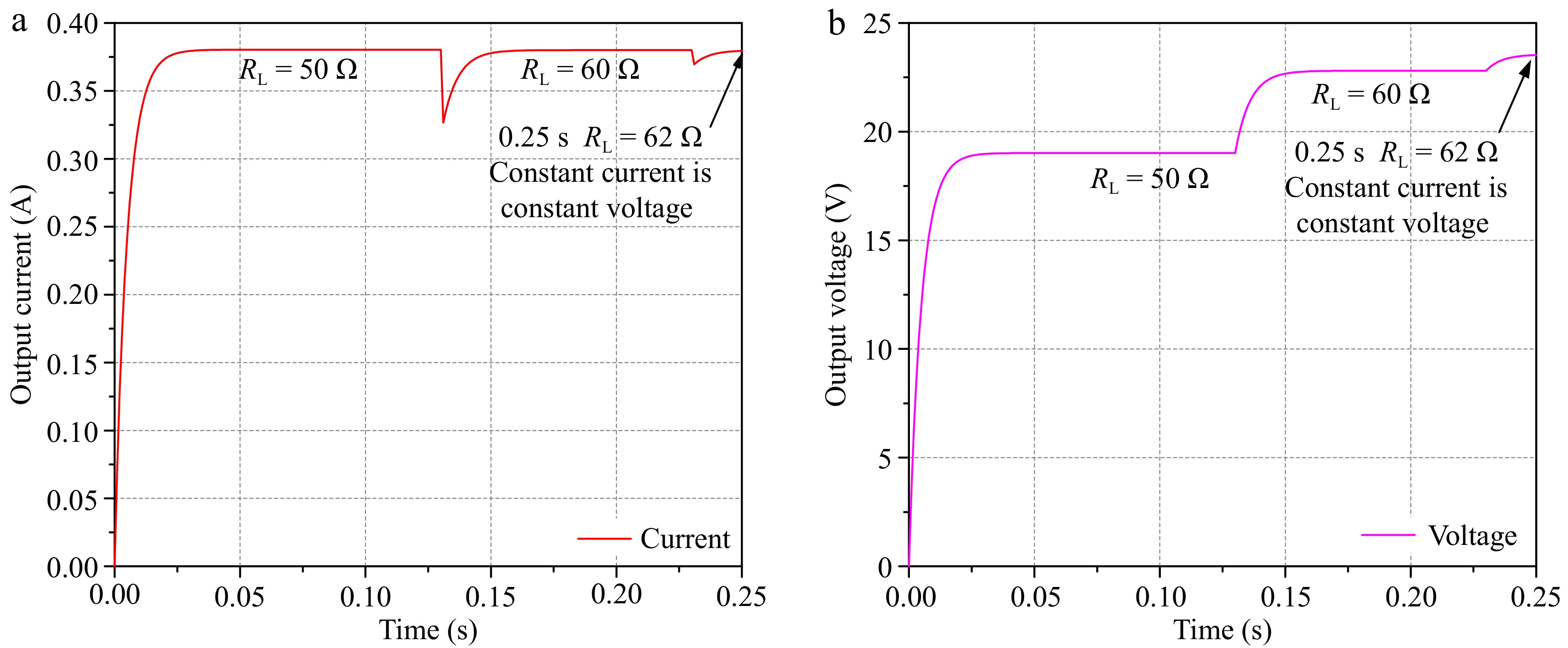
Figure 8.
Current-voltage diagram in constant-current mode. (a) Current. (b) Voltage.
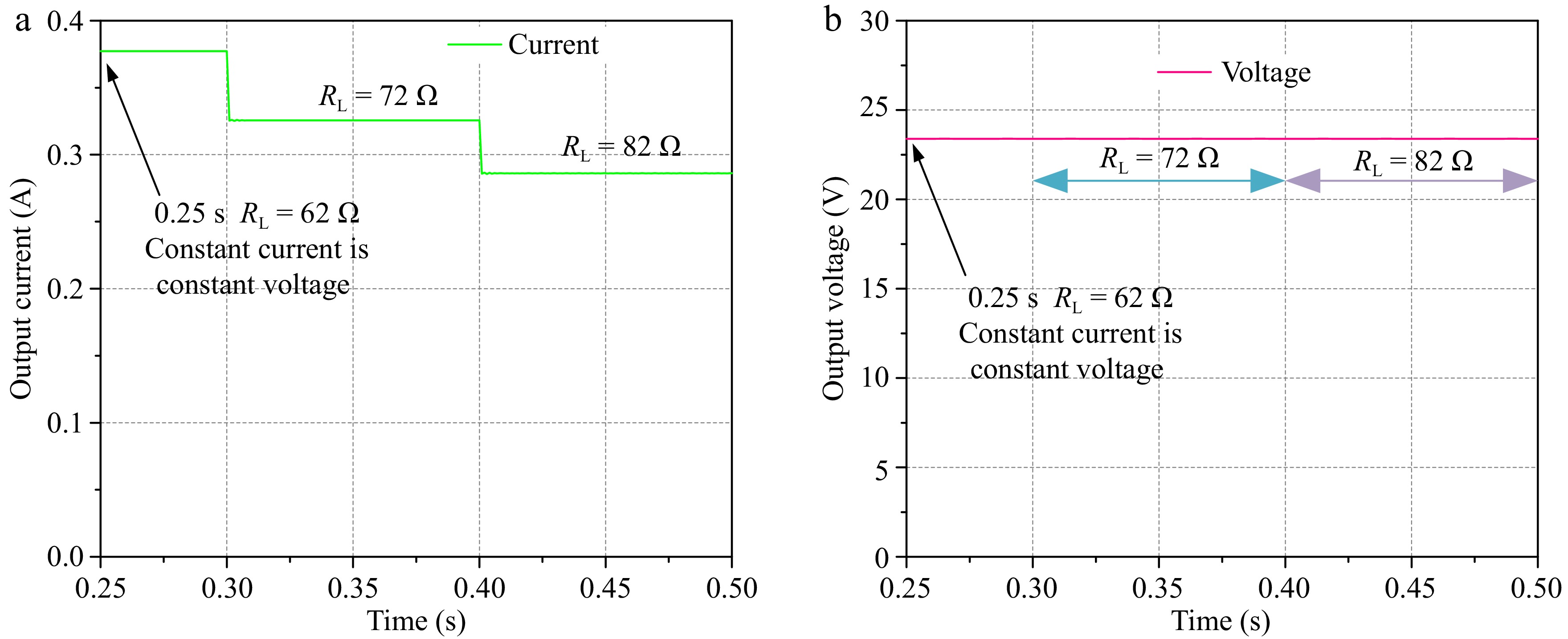
Figure 9.
Current-voltage diagram in constant-voltage mode. (a) Current. (b) Voltage.
It is important to note that when the charging voltage reaches the desired value, the resonance frequency is adjusted via the transmitter-side controller without using wireless communication. Instead, the load resistance and charging current are estimated based on known parameters, allowing for an estimation of the charging voltage, which serves as the criterion for frequency switching.
According to Fig. 8, it can be seen that before 0.25 s, the system is able to output a constant charging current of 0.38 A, but as the increase of the load resistance value, the charging voltage increases and when the load resistance value is 62 Ω at 0.25 s, the charging voltage reaches 23 V, then system enters into the CV charging mode.
As illustrated in Fig. 9, when the system is in the transient state at 62 Ω, the charging current is approximately 0.38 A, and the charging voltage is 23 V. After the system transitions to constant-voltage charging, the charging current gradually diminishes with the augmentation of load resistance. Although the charging voltage fluctuates slightly, the fluctuation is negligible and can be approximated as constant-voltage charging.
Since the switching criterion for the resonant frequency in this study is based on whether the estimated charging voltage reaches 23 V, Fig. 10 presents the waveform of the actual charging voltage and the predicted voltage around 0.25 s (when the resonant frequency is switched). It is apparent from Fig. 10 that the actual charging voltage is in high agreement with the predicted charging voltage, which verifies the rationality of the adopted methodology.
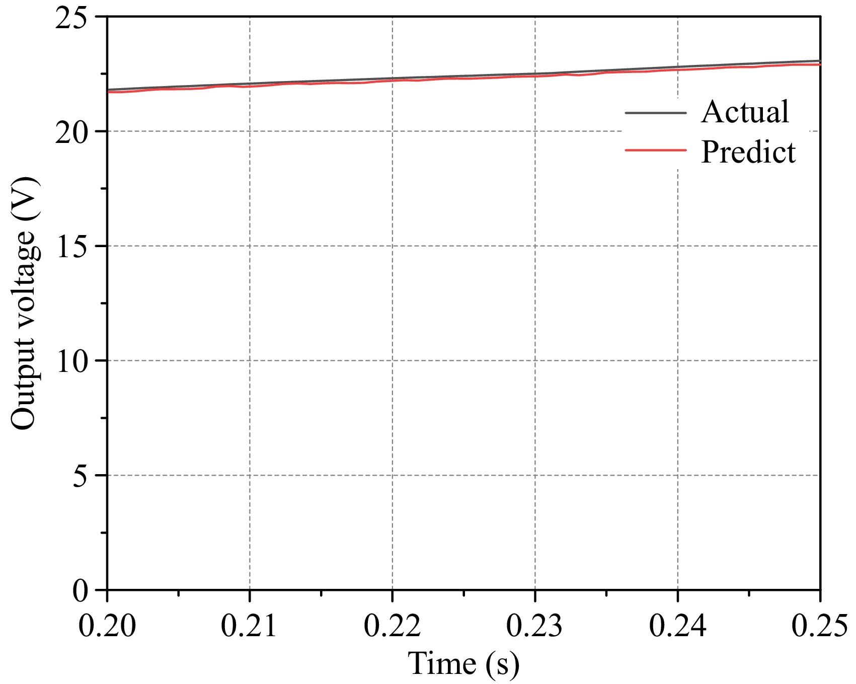
Figure 10.
Predicted and actual voltage waveforms at frequency switching.
According to Figs 5a and 6a, it can be concluded that in CC mode, when the system running at resonance, the total input impedance Zin is zero, and the current and voltage generated by the inverter's output exhibit Zero Phase Angle (ZPA) characteristics, as illustrated in Fig. 11a. In CV mode, the impedance angle is approximately 30° (with the current lagging the voltage by about 30°) when the system running at resonance, which prevents the realization of ZPA characteristics; however, soft switching can still be achieved, as illustrated in Fig. 11b.
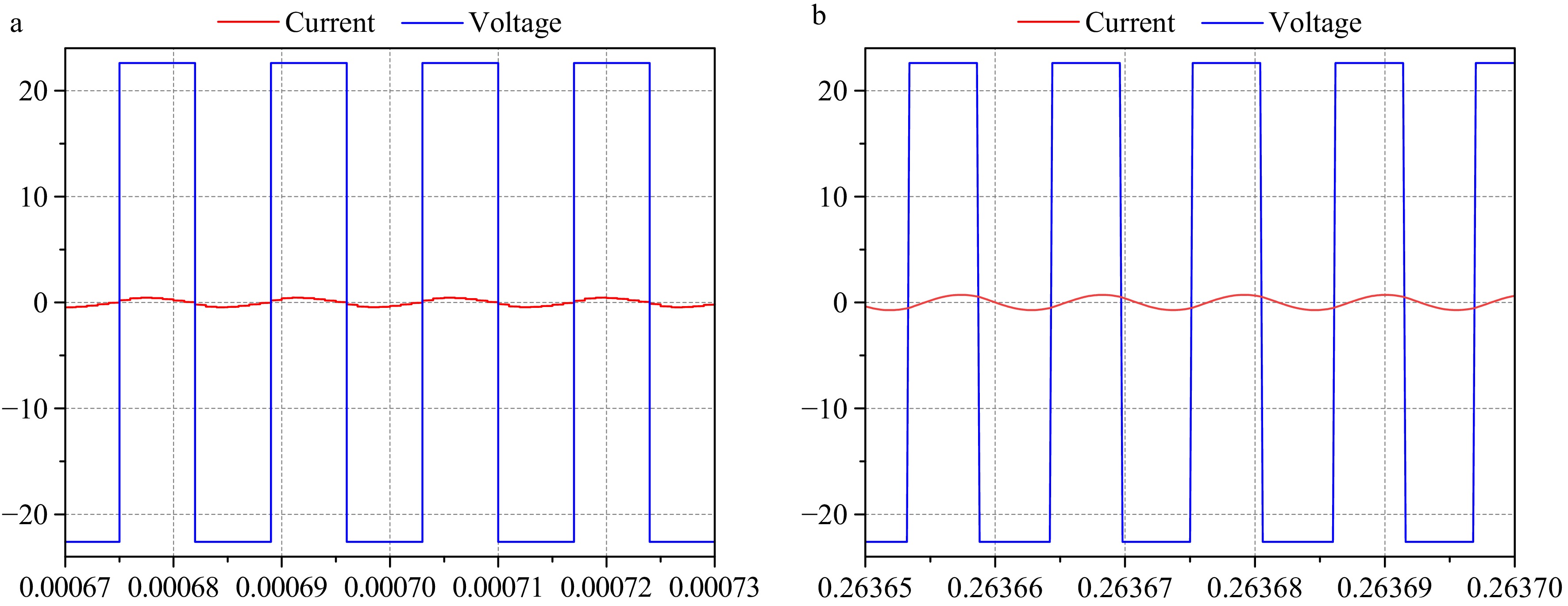
Figure 11.
Voltage-current waveform of inverter output. (a) CC. (b) CV.
Experimental verification
-
To verify the above theoretical analysis, the experimental platform shown in Fig. 12, is built on the basis of simulation verification.
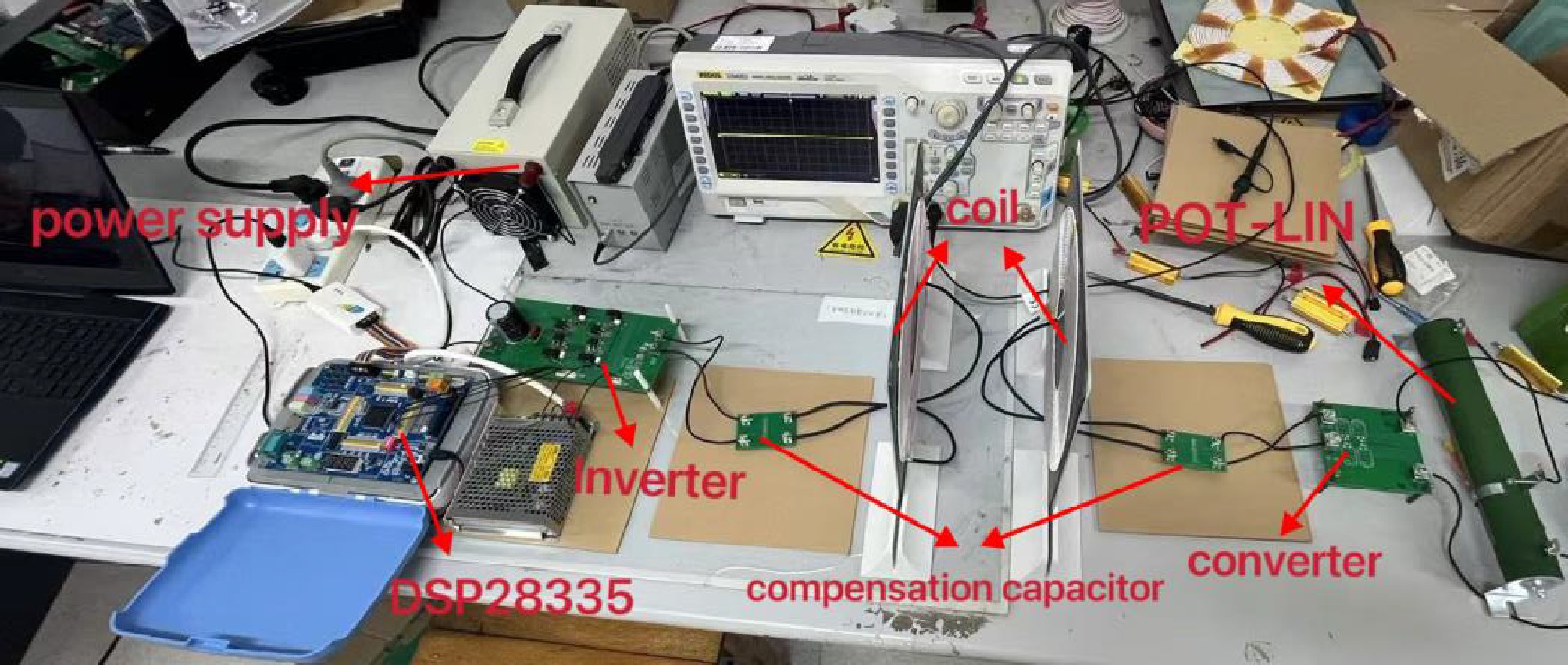
Figure 12.
Experimental platforms.
Figure 13a shows the experimental waveforms of inverter output voltage Uin and inverter output current Iin in CC mode, and Fig. 13b shows the current-voltage waveforms in CC mode.
From Fig. 13b, it can be seen that when the load resistance value is 25 Ω, the output current of the system is 0.38 A, with the increase of the load resistance value to 45 Ω, the voltage rises from 10 to 16 V, but the output current is still 0.38 A, and the system realizes the CC output.
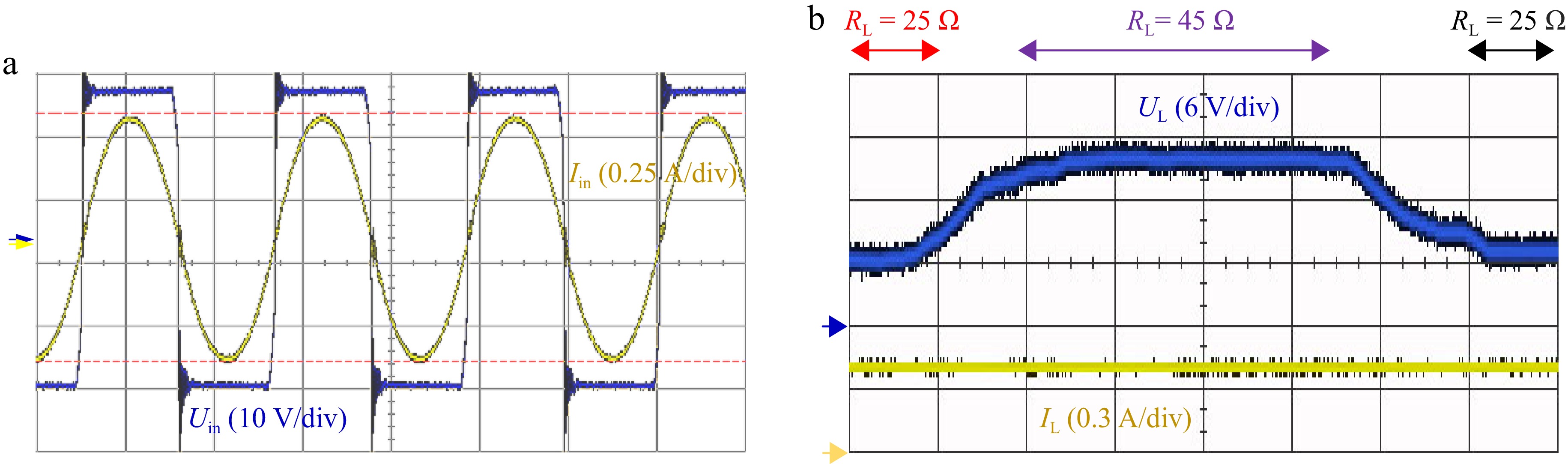
Figure 13.
Experimental diagram of the system in CC mode. (a) Inverter voltage and current phase. (b) Load current and voltage at constant current output.
Figure 14a shows the experimental waveforms of inverter output voltage Uin and inverter output current Iin in CV mode, and Fig. 14b shows the current-voltage waveforms in CV mode.
From Fig. 14b, it can be seen that when the load resistance value is 95 Ω, the output voltage of the system is 23 V and the output current is 0.2 A. When the load resistance value is increased to 125 Ω, the output current of the system is reduced to 0.04 A, and the output voltage is still 23 V, which realizes the CV output.
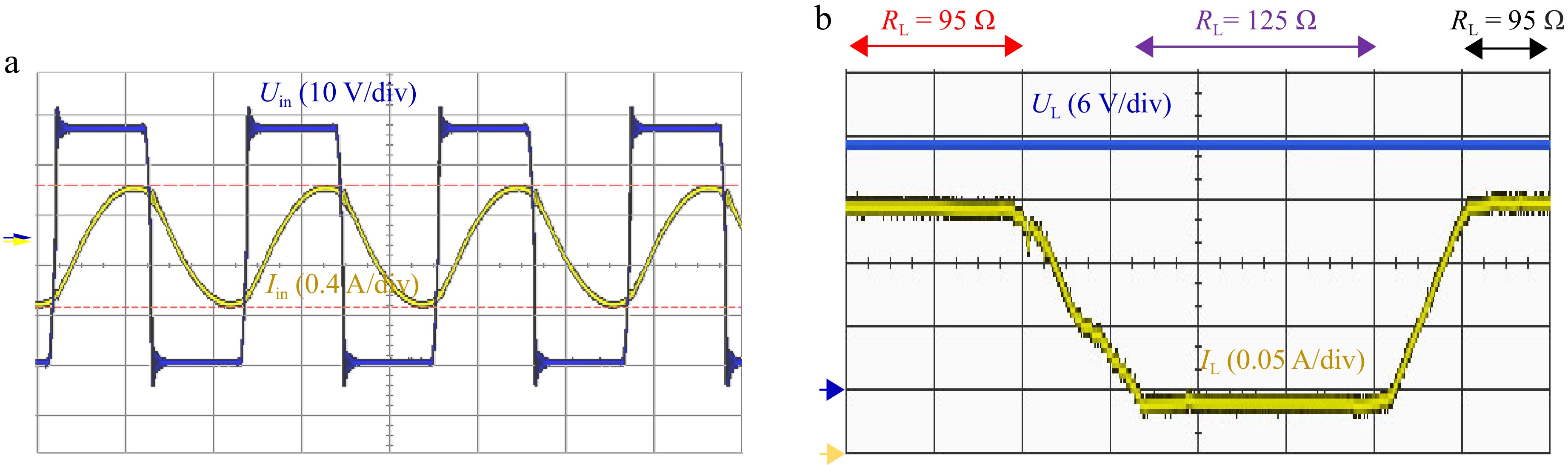
Figure 14.
Experimental diagram of the system in CV mode. (a) Inverter voltage and current phase. (b) Load current and voltage at constant voltage output.
Finally, the efficiency of the system designed in this paper is analyzed, as illustrated in Fig. 15, the efficiency of the system can be obtained and is higher in CC mode due to the ZPA characteristics of the system, which reached 96.5%, and in CV mode due to the presence of small impedance angle, the efficiency of the system reached 95.5%.
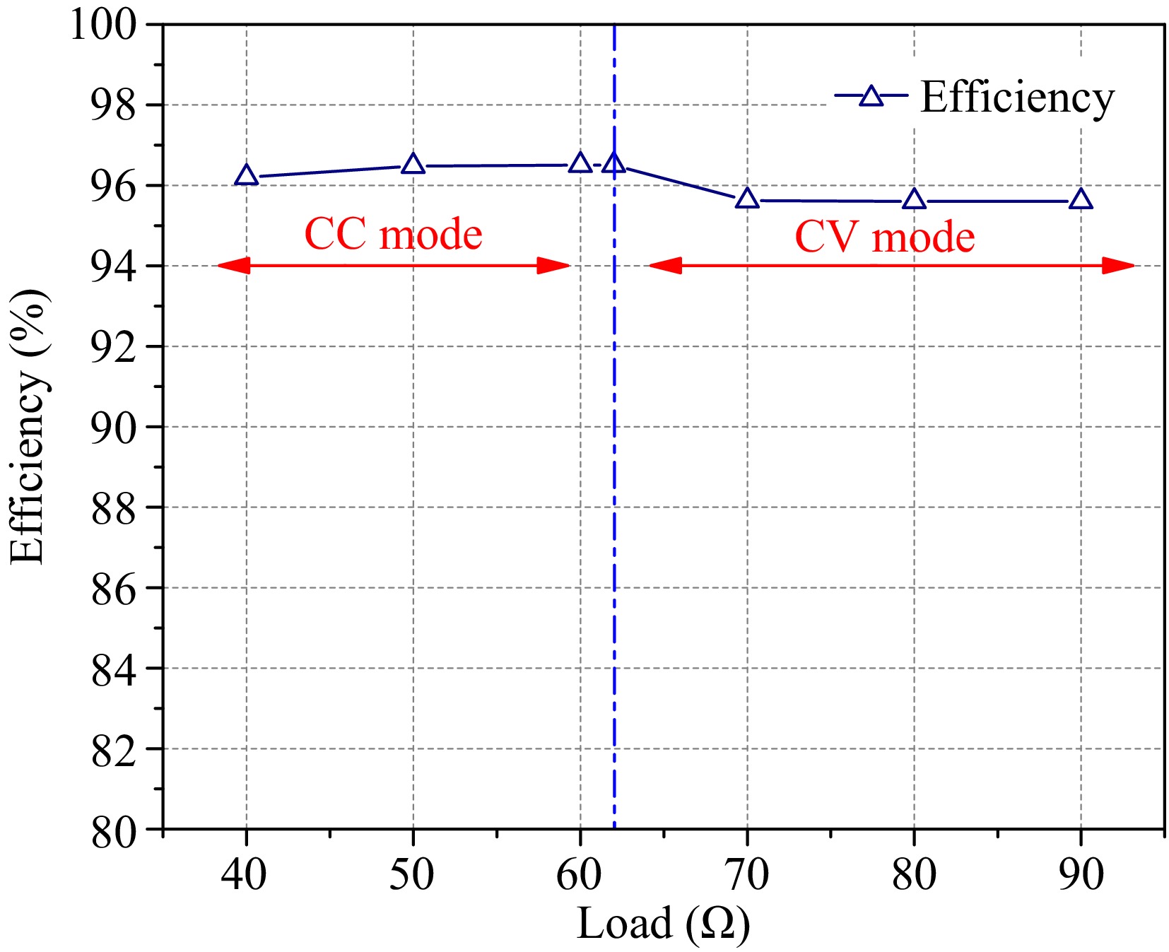
Figure 15.
Efficiency of WPT system with S/S structure.
The efficiency loss of the system is analyzed as shown in Fig. 16, and the efficiency loss is mainly concentrated on the inverter, compensation network, coupler, and rectifier. Since the inverter uses four IGBTs, the operating frequency of the system is not the best operating frequency of IGBTs, so the loss is mainly concentrated in the inverter, but the ZPA characteristics of the system in constant current mode and the ability to realize soft switching in constant voltage mode do not make the system efficiency loss too high; secondly, there is also a loss because the secondary coil can not completely absorb all the power of the primary coil. The rectifier and compensation network also have small losses.
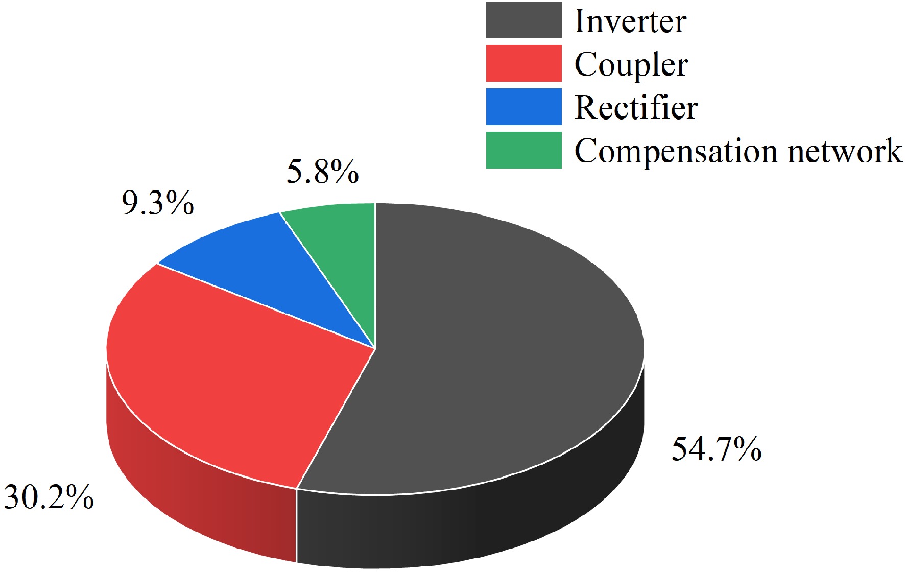
Figure 16.
Analysis of efficiency losses.
To demonstrate the superiority and innovation of the proposed system design methodology, the WPT technology proposed in this study has undergone a detailed performance comparison with systems documented in existing literature. The detailed comparison results are presented in Table 2. It can be seen that the system designed in this text both uses fewer compensating components and compensates for the shortcomings in the design of other methods.
Table 2. Comparison of CC and CV output WPT systems.
-
Most of the existing WPT systems rely on wireless communication to realize the switching of operating modes, which puts high requirements on the stability and complexity of the communication system, is susceptible to external interference and may lead to control failure or efficiency degradation, especially under dynamic loads. By switching the resonant frequency without wireless communication and directly utilizing the resonant network characteristics to achieve CC and CV charging, not only the system architecture is simplified and the cost is reduced, but also the robustness of the system is improved. This method can realize more efficient and stable power transmission, which has obvious advantages over traditional methods.
Through this study, the necessity of wireless communication in WPT systems has been reevaluated, providing new design ideas for realizing a more simplified and reliable WPT system. This technique breaks the dependence on traditional communication links and makes WPT applications possible in resource-constrained or high-interference environments.
The study mainly verifies the feasibility of the method of switching resonant frequency, but it has not yet fully explored how to realize the optimal frequency switching strategy under dynamic loading, which can be thoroughly investigated in this direction in the future, and to validate the robustness of the method in more complex scenarios, such as high power and long transmission distance, and to promote its application in real products.
-
This paper proposes an S/S compensated WPT system to enable battery charging in both constant current and current voltage modes by switching between two specific frequencies. Through circuit structure analysis and theoretical derivation, the system can achieve constant current and current voltage outputs at two fixed resonant frequencies without reconfiguring the circuit structure and without complex closed-loop control. Additionally, an output voltage estimation method is employed, which does not require wireless communication. Simulation results and experimental results validate that the designed system can achieve a charging output of 0.38 A/23 V, with minimal error between the actual charging output voltage and the estimated output voltage. Finally, the system's efficiency is analyzed, with an efficiency of 96.5% in CC mode and 95.5% in CV mode.
This work was supported in part by the Natural Science Foundation of Shangdong Province (Grant No. ZR2022ME214).
-
The authors confirm contribution to the paper as follow: study conception and design: Guo Z, Li Z; data acquisition and data collation: Guo Z, Li Z, Yu H, Zhang H; analysis of simulation results: Guo Z, Li Z, Nai J, Chen S; writing manuscript review and editing: Guo Z, Li Z, Liu R; access to funds: Zhang M. All authors have read and agreed to the final version of the manuscript.
-
All data generated or analyzed during this study are included in this published article.
-
The authors declare that they have no conflict of interest.
- Copyright: © 2025 by the author(s). Published by Maximum Academic Press, Fayetteville, GA. This article is an open access article distributed under Creative Commons Attribution License (CC BY 4.0), visit https://creativecommons.org/licenses/by/4.0/.
-
About this article
Cite this article
Guo Z, Li Z, Yu H, Zhang H, Nai J, et al. 2025. WPT system for constant current and constant voltage charging based on switched resonant frequency. Wireless Power Transfer 12: e013 doi: 10.48130/wpt-0025-0009 

WPT system for constant current and constant voltage charging based on switched resonant frequency
- Received: 25 November 2024
- Revised: 24 February 2025
- Accepted: 18 March 2025
- Published online: 09 May 2025
Abstract: This paper designs and implements an innovative WPT system that possesses the capability to seamlessly switch between constant current (CC) and constant voltage (CV) outputs, thereby fully satisfying the various charging requirements of batteries for both CC and CV. An S/S compensated WPT system is proposed that enables battery charging in both CC and CV by switching between two specific frequencies. In addition, load estimation and output current estimation are employed to estimate the output voltage. The output voltage will be used as a criterion for the conversion of the operating frequency of the CC to the operating frequency of the CV. The system is simple and does not require complex control strategies, primary and secondary side communication, or additional devices to reconfigure the circuit topology. The charging output of the proposed system can reach 0.38 A/23 V based on an S/S topology. Both through theoretical analysis and computer simulations, the feasibility of the proposed WPT system has been verified. The experimental results show that a CC output of 0.38 A and a CV output of 23 V can be realized by switching the resonant frequency at a constant input voltage.
-
Key words:
- WPT /
- Constant current /
- Constant voltage /
- No communication /
- Switching frequency