


-
In hazardous environments such as coal mines and petrochemical facilities, where explosive gases or dusts are present, electrical equipment must comply with intrinsic safety (IS) standards to prevent ignition. Intrinsically safe systems are designed such that even under fault conditions, the electrical energy available in the system is insufficient to cause ignition of the surrounding explosive atmosphere. With the advancement of society and technology, wireless power transfer (WPT) technology has become a significant research direction in modern power transfer systems[1,2]. It has been widely applied in various fields such as implanted medical devices[3,4], electric vehicles[5,6], portable communication devices[7], and smart homes[8]. In particular, in hazardous environments like underground coal mines, traditional wired power transfer methods pose numerous inconveniences and safety hazards. But their deployment in underground coal mines remains challenging due to the unique environmental conditions. Existing systems often struggle with issues such as voltage fluctuations, inadequate protection circuits, and insufficient filtering performance, which undermine their reliability and safety. Moreover, the current national standard (GB/T 3836.1-2021 Explosive Atmospheres—Part 1: Equipment—General Requirements) imposes strict limitations on the power threshold of radio frequency equipment in explosive environments, which is based on low-frequency experimental data from the 1970s. WPT technology, with its advantages of contactless transfer, electrical isolation, and flexible arrangement, has gained widespread attention[9−11].
In the field of WPT, considerable research has been devoted to improving transfer efficiency and stability. For instance, traditional LC compensation structures are widely used in various WPT systems due to their simplicity[12]. However, the resonance frequency of the LC compensation structure varies with load changes, leading to reduced system efficiency. In contrast, the LCL compensation structure, although more complex, maintains a constant resonance frequency under load variations. This ensures that the front-end inverter circuit always operates in a soft-switching state. Consequently, it improves system efficiency and reduces switching losses[13−15]. Additionally, single-ended flyback converters are widely used in low-power WPT systems due to their simple structure and low cost. However, the omission of the filter inductor often adversely affects the lifespan of the capacitor[16].
Despite significant progress in improving the efficiency and stability, there are still shortcomings in protection circuit design and filtering effects, especially in the special environment of underground coal mines. Particularly, in the context of large voltage fluctuations in underground power grids, designing effective protection circuits to enhance system reliability and safety remains an urgent issue. Furthermore, existing WPT systems lack targeted optimization research in the parameter design of inductors and capacitors.
To address these issues, this study proposes a WPT system based on a single-ended flyback converter and focuses on the optimization design of its protection and filter circuits. First, a CLC filter circuit is designed, significantly extending the capacitor's lifespan and improving the filtering effect through the rational selection of capacitor parameters. Second, a novel undervoltage and overvoltage protection circuit based on the LM339 comparator is designed, capable of quickly responding and protecting the system during significant voltage fluctuations in the power grid, ensuring stable operation. Finally, the effectiveness of the designed circuits is validated through simulation and experimentation, showing that the proposed WPT system has significant advantages in terms of safety and reliability.
The main innovations of this study include:
(1) Proposing an optimized CLC filter circuit design that extends capacitor life and improves filtering effectiveness.
(2) Designing an undervoltage and overvoltage protection circuit based on the LM339 comparator that effectively addresses voltage fluctuations in underground power grids.
(3) Validating the effectiveness of the designed circuits through simulation and experimentation, ensuring system safety and reliability.
This study aims to address these limitations by proposing an optimized WPT system design based on a CLC filter circuit and a protection circuit using the LM339 comparator. Theoretical analysis and experimental results demonstrate significant improvements in stability and safety, laying the groundwork for future technological breakthroughs in this field.
-
The system begins with an AC input filtered by an electromagnetic interference (EMI) circuit to suppress electromagnetic interference, ensuring stable operation in complex mining environments. The filtered AC is then rectified into DC and fed into a high-frequency inverter employing a voltage-type full-bridge topology with phase-shift control. This stage improves power conversion efficiency and reduces system volume for easier deployment in confined spaces.
The high-frequency AC is wirelessly transmitted via magnetic resonant coupling, enhancing safety and eliminating the need for physical connectors in hazardous areas. At the receiving end, a high-frequency rectifier and an intrinsically safe DC-DC converter provide a stable DC output, with built-in dual overvoltage and overcurrent protection mechanisms to meet safety requirements in explosive atmospheres. The system delivers reliable power to support intrinsically safe mining equipment.
The main circuit, as shown in Fig. 1, starts with an AC passing through filter capacitor C1 to remove high-frequency interference. Next, the rectifier bridge circuit, composed of rectifier diodes (D1, D2, D3, D4), converts the AC to DC. The rectified DC then enters the inverter circuit, where inverter switching elements (S1, S2, S3, S4) and freewheeling diodes (D5, D6, D7, D8) convert the DC to high-frequency AC.
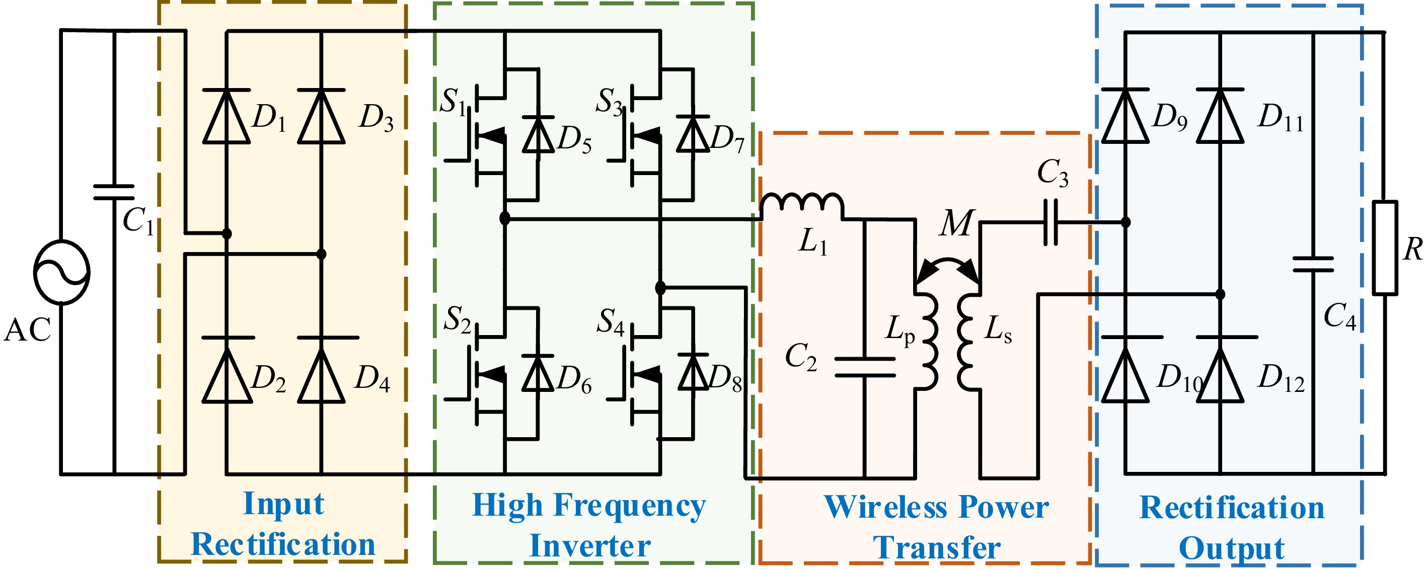
Figure 1.
Main circuit topology.
The high-frequency AC generates a magnetic field through the primary transmitting coil (Lp), which couples to the secondary receiving coil (Ls) to achieve wireless power transfer. M represents the mutual inductance. Resonant capacitors C2 and C3 adjust the resonant frequency to enhance transfer efficiency. The received high-frequency AC is converted back to DC through rectifier diodes (D9, D10, D11, D12), filtered by capacitor C4 to remove high-frequency ripple, and finally outputs a stable DC voltage to supply electrical equipment (equivalent load R) in the mine.
The system achieves safe, efficient, and stable wireless power transfer in the mining environment through the collaborative work of each module.
The LCL-S compensated topology ensures series resonance on the primary side and parallel resonance on the secondary side. This structure effectively decouples the resonant condition from the resistive load magnitude, allowing the system to maintain resonance even when the load power changes:
$ \left\{ \begin{gathered} {\omega _{\text{r}}}{L_{\text{p}}} = {\omega _{\text{r}}}{L_{\text{1}}} = \dfrac{1}{{{\omega _{\text{r}}}{C_{\text{p}}}}} \\ {\omega _{\text{r}}}{L_{\text{s}}} = \dfrac{1}{{{\omega _{\text{r}}}{C_{\text{s}}}}} \\ \end{gathered} \right. $ (1) where, ωr is the frequency of electric energy output by the inverter.
However, if the load exhibits inductive or capacitive characteristics, the resonance condition will shift. To analyze this, consider the total secondary-side impedance Zsec:
$ {Z_{\sec }}\left( s \right) = \left( {\dfrac{1}{{s{C_2}}} + s{L_2} + {Z_{{\text{load}}}}} \right) $ (2) Assuming the load has a complex impedance Zload = R + sLload + 1/sCload, the total resonant frequency fr of the LCL circuit becomes dependent on the combined impedance. For ideal resonance, the imaginary part of Zsec should be zero, which leads to the condition:
$ {Im} \left[ {{Z_{\sec }}} \right] = {\omega _{\text{r}}}{L_2} - \dfrac{1}{{{\omega _{\text{r}}}{C_2}}} + {\omega _{\text{r}}}{L_{{\text{load}}}} - \dfrac{1}{{{\omega _{\text{r}}}{C_{{\text{load}}}}}} = 0 $ (3) From this, it is evident that significant inductive or capacitive loads shift the resonant frequency away from its nominal point, degrading the compensation condition. Therefore, the LCL topology can maintain resonance when the load remains purely resistive or has weak reactive components (i.e., Lload << L2, Cload << C2). In practical applications, the load behaves approximately resistively or with minimal reactance, satisfying the resonance condition.
Design of the input filter circuit
-
The system is designed with an EMI rectification filter circuit, which not only suppresses the impact of high-frequency interference from the power grid on the equipment but also mitigates the impact of the equipment's high-frequency switching tubes on the AC power grid. This is beneficial for the safe operation of the equipment and also helps stabilize the quality of the power grid voltage. The EMI filter circuit is shown in Fig. 2.
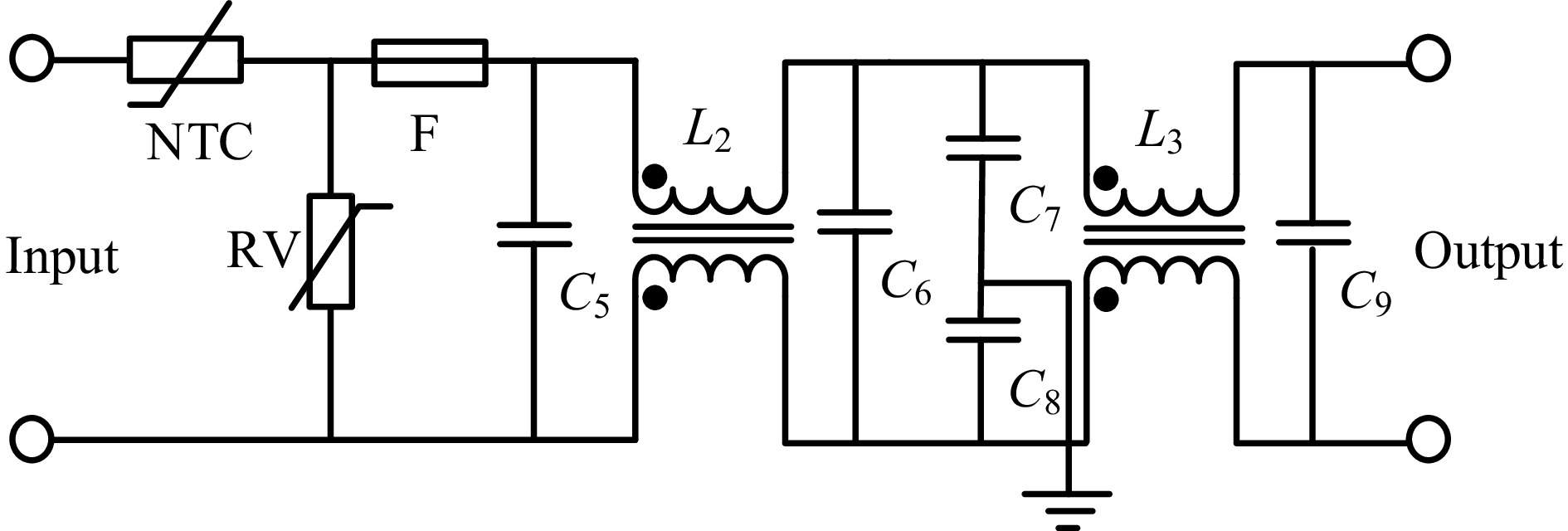
Figure 2.
Rectification and filtering circuit diagram.
The system's filter circuit incorporates a two-stage composite EMI filter, which includes a protection circuit with a thermistor (NTC), a varistor (RV), and a fuse (F). The NTC, which limits large inrush currents at startup by decreasing its resistance as it heats up, enhances safety. The RV protects against overvoltage by rapidly increasing current flow, thereby clamping the voltage to a stable value, contributing to the overall safety of the intrinsically safe wireless power transfer system.
Following the protection circuit are common-mode chokes (L2, L3) and filter capacitors (C5−C9). The two coils of L2 have the same magnetic flux direction. When common-mode interference occurs, the total inductance of L2 increases rapidly, greatly obstructing the common-mode signals. The selection of L2's inductance depends on the rated current of the circuit. Under the same frequency and voltage drop, the larger the current, the smaller the required inductance. The capacitors (C5−C9) are safety capacitors, which are generally used in anti-interference filter circuits and will not fail by breakdown. Safety capacitors are divided into X and Y types. X-type safety capacitors are connected between the live wire and the neutral wire. In this EMI filter circuit, C5, C6, and C9 are all X-type safety capacitors, with capacities ranging from 0.01 to 0.47 μF, filtering differential mode interference. C7 and C8 are connected between the live wire and the ground wire and the neutral wire and the ground wire, respectively. They are Y-type safety capacitors with capacities ranging from 2,200 pF to 0.1 μF, suppressing common-mode interference. This system's filter circuit adopts more effective two-stage filtering.
Following the input filter circuit is the input rectifier circuit. This system uses an uncontrolled rectifier circuit composed of four diodes. Afterward, capacitor filtering smooths the voltage to output DC with minimal ripple, serving as the input for high-frequency inversion.
Rectifier circuit design
-
The rectifier circuit of this system uses an uncontrolled rectifier circuit primarily composed of diodes. This rectifier circuit outputs significant ripple, and after high-frequency inversion, a good sine wave cannot be obtained on the transmitting coil. Therefore, a filter capacitor is added after the rectifier circuit.
According to the design of this system, the 127 V AC voltage underground needs to pass through the rectifier circuit before it can be used. The subsequent circuits rely on the rectifier circuit to provide power, so a reliable regulated power supply is a prerequisite for the system's operation. The main parameters to consider for the uncontrolled rectifier are its rated voltage, current, and power. Given the instability and wide voltage variation of the mine power grid, with a voltage fluctuation range of ± 15%, the maximum input voltage Vinmax is chosen to be 150 V. Considering the safety margin, a factor of 1.5 is applied using the following equation:
$ {V_{{\text{BF}}}} = 1.5 \times \left( {\sqrt 2 \times {V_{{\text{inmax}}}}} \right) $ (4) The voltage withstand value VBF of the rectifier module should be greater than 318 V. The maximum rated current of the rectifier module is determined by the system's maximum output power and the minimum input current. Considering a ± 15% voltage fluctuation, the minimum input voltage is 105 V.
$ {I_{{\text{BF}}}} = \dfrac{{{P_0}}}{{\eta \times {V_{{\text{inmin}}}}}} $ (5) According to Eq. (5), the rated input current IBF of the uncontrolled rectifier module is calculated to be 0.14 A. Taking the safety margin and the impact of power grid voltage fluctuations into account, the input current is chosen to be 1 A.
Inverter circuit design
-
As shown in Fig. 1, the system employs a voltage-type full-bridge inverter circuit. This circuit has a low switching current, making it suitable for high-power applications. Based on the voltage level requirements and topology of the system, the full-bridge inverter can effectively regulate voltage through phase-shift control.
Due to the low power level of the mine-used intrinsically safe wireless power transfer system, the inverter circuit needs to use phase-shift control to reduce the voltage level. In operation, S1 and S2 switches are complementary, and S3 and S4 switches are complementary, with a certain angle α. The output voltage of the switching tube is only related to α. The phase-shift control method is simple and effective, capable of adjusting the output voltage value well and achieving soft switching better. The output voltage Uout for the phase-shift control method is given by:
$ {U_{{\text{out}}}} = \dfrac{{4{U_{{\text{in}}}}}}{\pi }\cos \dfrac{\alpha }{2}\sin \omega t $ (6) where, Uin represents the input voltage, and ω represents the angular frequency of the switching signal. The maximum peak voltage UDS that the switching tube can withstand is calculated to be 127 V, and the maximum peak current ID is 4 A.
The 1.5 times safety margin was determined based on industry best practices and historical data from similar systems operating in hazardous environments. Therefore, considering a safety margin of 1.5 times, UDS = 200 V and ID = 6 A. Therefore, when selecting a power switch tube, its input current, maximum withstand voltage, power, and other parameters should be considered. The required frequency for this system is relatively high. The MOS transistor is selected due to its unipolar voltage drive and high operating frequency. However, it has a large on-resistance, which increases with the voltage withstand value. The MOS transistor selection should meet the working frequency and withstand voltage requirements, and its parasitic capacitance should be small.
Magnetic circuit structure design
-
For a wireless power transfer system, the transmitting and receiving coils are critical components. Factors such as the size, shape, and relative position of the coils significantly affect the transfer power efficiency of the system. Common wireless power transfer systems typically use separable transformer-type, planar, or solenoid coils, each with its own advantages.
The separable transformer-type magnetic circuit offers superior magnetic coupling and efficient point-to-point energy transfer, enhancing power transfer efficiency, but it is bulky, material-intensive, and expensive. However, this structure occupies a large space, requires more materials, and is costly. The planar coil, with its thin profile, is easier to miniaturize but requires precise alignment of the two coils to achieve optimal performance. The solenoid coil has a uniform magnetic field distribution and good directionality, beneficial for long-distance, efficient transfer. The planar coil generates a weaker magnetic field than the solenoid coil with the same turns and size. However, its magnetic field is more concentrated near the plane of the coil.
Considering the special environment of underground mines, this system uses a planar coil structure. The planar coil not only helps in miniaturizing the system but also has a magnetic field distribution that makes it more suitable for underground applications. Although this structure requires strict control of the relative position of the two coils, keeping them parallel and coaxial to achieve the best transfer effect, it remains the most suitable choice for underground use.
Figure 3a shows the mutual inductance design structure when the two coils are parallel and coaxial. Figure 3b further illustrates the impact of position on transfer efficiency. The mutual inductance between the two coils is given by:
$ M = {\mu _0}\dfrac{{\sqrt {{r_{\text{D}}}{r_{\text{S}}}} }}{b}{n_0}{n_1}\left[ {\left( {2 - {b^2}} \right)K\left( b \right) - 2E\left( b \right)} \right] $ (7) $ b = \sqrt {\dfrac{{4{r_{\text{D}}}{r_{\text{S}}}}}{{{{\left( {{r_{\text{D}}} + {r_{\text{S}}}} \right)}^2} + {d^2}}}} $ (8) where, rS represents the radius of the transmitting coil, rD represents the radius of the receiving coil, n0 and n1 represent the number of turns of the transmitting and receiving coils respectively, d represents the distance between the coils, K(b) represents the complete elliptic integral of the first kind, and E(b) represents the complete elliptic integral of the second kind.
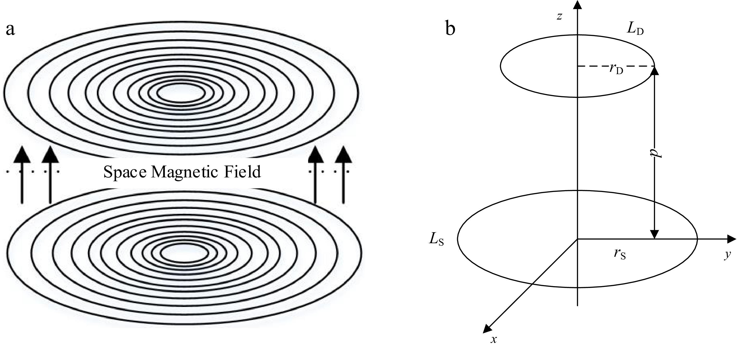
Figure 3.
Diagram of WPT coil. (a) Diagram of planar coil structure. (b) Diagram of parallel coaxial coil spatial structure.
By optimizing the coil design and layout, this system can achieve efficient and safe wireless power transfer in an underground environment.
-
To meet the stringent safety demands of underground power systems, this section details the design of an intrinsically safe flyback DC-DC converter, emphasizing structural simplification, electrical isolation, and compliance with national explosion-proof standards.
Selection and advantages of the flyback converter under intrinsic safety constraints
-
There are five common types of switching converters: single-ended flyback converter, single-ended forward converter, push-pull converter, half-bridge converter, and full-bridge converter. Among these, the single-ended flyback converter is characterized by its simple structure, low cost, suitability for low-power applications, strong electrical isolation capabilities, and high stability. The flyback converter reduces manufacturing and maintenance costs due to its fewer components and simplified design, making it ideal for cost-sensitive scenarios. It performs well in low-power outputs, meeting the needs of a mine's wireless power transmission system. Additionally, the flyback converter can achieve electrical isolation between input and output, enhancing system safety, which is especially important in high-safety-demand mine environments. The flyback converter also offers high stability and reliability in harsh environments, ensuring long-term stable operation of the system.
The single-ended flyback converter is an ideal choice for the mine wireless power transmission systems, balancing cost, design simplicity, stability, and safety. However, this converter is not suitable for systems with excessively high voltage.
As shown in Fig. 4, when Q is on, the transformer stores energy, and the capacitor supplies power to the load. When Q is off, the diode conducts, the transformer releases energy, supplying power to the load while charging the capacitor. The average output voltage of the system is UO.
$ {U}_{\text{O}}=\dfrac{D}{n(\text{1}-D)}\cdot {U}_{\text{i}} $ (9) where, Ui is the input voltage, n is the turns ratio of the converter, and D is the duty cycle.
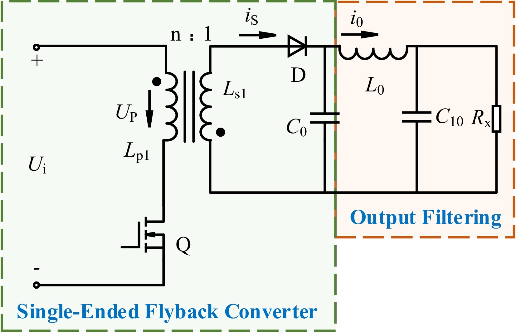
Figure 4.
Single-ended flyback converter with output filtering.
To ensure that the front-end wireless power transmission device can output the target DC voltage, this study selected an input voltage Ui = 20 V and a target output voltage Uo = 12 V, using a maximum duty cycle Dmax = 0.55. The calculation formula for the turns ratio n is obtained by:
$ n=\dfrac{{U}_{\text{i}}}{{U}_{\text{O}}}\cdot \dfrac{{D}_{\mathrm{max}}}{(\text{1}-{D}_{\mathrm{max}})} $ (10) Since the turns ratio must be an integer, choose n = 2. Based on the turns ratio and Eq. (7), the duty cycle is recalculated by D'max = 0.545.
The average primary coil current Ipdc under normal operating conditions is calculated by:
$ {I_{{\text{pdc}}}} = \dfrac{{{U_O} \times {I_O}}}{{\eta \times {U_i}}} $ (11) where, IO is the load current and η is the efficiency (assumed to be 0.8).
The peak values of the primary and secondary coil currents Ipmax and Ismax can be written as follows:
$ {I}_{\text{pmax}}=\dfrac{2{I}_{\text{pdc}}}{{D}_{\mathrm{max}}^{'}} $ (12) $ {I_{{\text{smax}}}} = n \times {I_{{\text{pmax}}}} $ (13) These results provide the necessary foundational data for further circuit design. To ensure normal operation, the inductance values of the primary and secondary coils, Lp and Ls, are calculated as follows:
$ {L_{\text{p}}} = \dfrac{{{U_{\text{i}}} \times {D_{{\text{max}}}}}}{{{I_{{\text{pmax}}}} \times {f_{\text{s}}}}} $ (14) $ {L_{\text{s}}} = \dfrac{{{L_{\text{p}}}}}{{{n^2}}} $ (15) where, fs is the switching frequency. These calculations determine the turns ratio and inductance values of the transformer. This ensures the system operates stably and efficiently under the target voltage and current conditions, while meeting the intrinsic safety requirements of the mine wireless power transmission system. This series of designs and calculations provides a reliable theoretical basis for the practical application of the system.
As mentioned earlier, the transformer of the single-ended flyback converter has a dual role. To reduce the power supply volume, the filter inductor is often omitted in the design. However, this design causes the instantaneous large current generated by the transformer to be directly applied to the capacitor, adversely affecting the capacitor's lifespan. Therefore, a CLC filter is added in this system to extend the service life of the capacitor, as shown in Fig. 5.
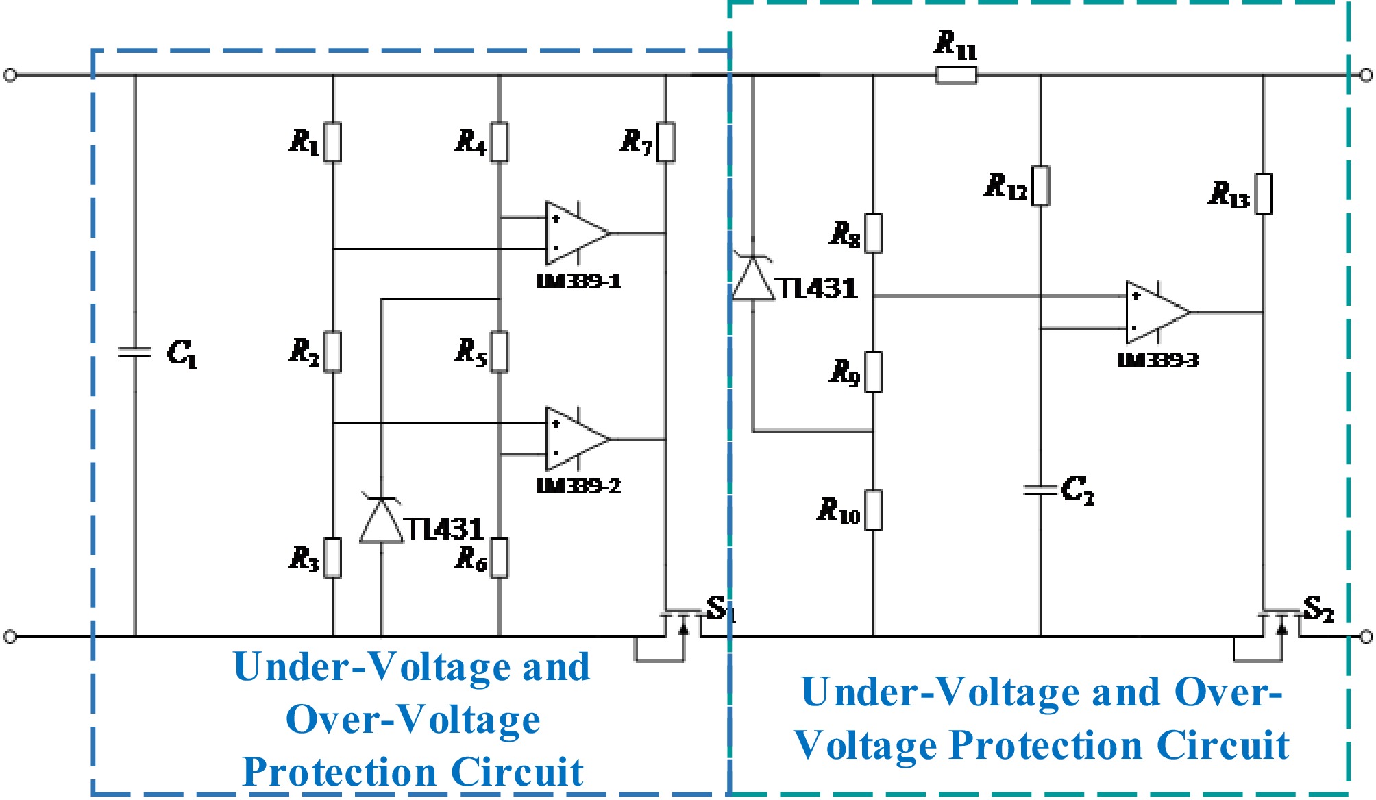
Figure 5.
Single-ended flyback converter with output filtering.
Typically, in capacitor parameter design, C0 is chosen with a larger capacitance value to filter low-frequency ripple, while C10 is chosen with a smaller capacitance value to filter high-frequency ripple. From a safety perspective, the CLC filter structure also effectively reduces the spark energy during circuit faults. The inductor L0 can effectively slow down the discharge speed of the front-stage capacitor, achieving good filtering effects even with a small C10 value.
In summary, the CLC filter not only extends the lifespan of the capacitor and improves filtering effects but also enhances the safety. This section is placed before the system's multiple protection circuits to ensure the overall reliable operation of the system.
Under-voltage and over-voltage protection circuit design
-
In underground power systems, voltage fluctuations can stress electronic devices, risking damage. To improve reliability and safety in hazardous coal mines, it's crucial to define strict voltage limits. This system uses an LM339-based protection circuit, which features four comparators and switches between high and low levels with a conversion time of 1.4 μs, providing effective under-voltage and over-voltage protection.
The protection scheme ensures compliance with intrinsic safety thresholds, and its modular integration with the flyback topology allows for rapid fault isolation and voltage stabilization, which is particularly beneficial in unpredictable underground settings.
As shown in Fig. 5, the under-voltage and over-voltage protection circuit consists of over-voltage and under-voltage detection circuits and an action circuit, with the reference voltage provided by the TL431. The over-voltage protection reference voltage Vref1 is supplied by the TL431 to the non-inverting input of LM339-1, while the inverting input voltage V1 is derived from the voltage divider resistors R1 and R2 + R3:
$ \dfrac{{{R_{\text{1}}}}}{{{R_{\text{2}}} + {R_{\text{3}}}}} = \dfrac{{{V_{{\text{in}}}} - {V_{{\text{ref1}}}}}}{{{V_{{\text{ref1}}}}}} $ (16) where, Vin is the input voltage of the under-voltage and over-voltage protection circuit, and Vref1 is the voltage between the cathode and anode of the TL431, which is also the non-inverting input of LM339-1. Choosing R1 = 9.7 kΩ and R2 + R3 = 2.3 kΩ, the circuit operates normally when the inverting input voltage of the comparator LM339-1 is less than 2.5 V. In this state, the output voltage of LM339-1 is pulled to a high level by R7, keeping the S transistor closed, and the circuit outputs normally. When over-voltage occurs, the inverting input voltage of LM339-1 exceeds 2.5 V, causing LM339-1 to output a low voltage, opening the S transistor and disconnecting the circuit output. Once the voltage returns to normal, the S transistor closes, and the circuit resumes normal output.
For under-voltage protection, the reference voltage Vref2 is provided by the TL431 and fed to the inverting input of LM339-2 after voltage division. With R4 = 5 kΩ, R5 = R6 = 1 kΩ, and the non-inverting input voltage V2 is obtained from the voltage divider resistors R2 and R3:
$ \dfrac{{{R_2}}}{{{R_3}}} = \dfrac{{{V_1} - {V_{{\text{ref2}}}}}}{{{V_{{\text{ref2}}}}}} $ (17) where, V1 is the inverting input voltage of LM339-1 and Vref2 = Vref1/2. With R2 = 1 kΩ, R3 = 1.3 kΩ, the circuit operates normally when the non-inverting input voltage of the comparator is greater than 1.25 V. The output voltage of LM339-2 is pulled to a high level by R7, keeping the S transistor closed, and the circuit outputs normally. When under-voltage occurs, the non-inverting input voltage drops below 1.25 V, causing LM339-2 to output a low voltage, opening the S transistor and cutting off the output. Once the voltage returns to normal, the S transistor closes, and the circuit resumes normal output.
Over-current protection circuit design
-
Intrinsically safe circuits must include at least two sets of protection circuits in series to ensure continued function if one fails. Figure 5 illustrates the protection circuit diagram, which includes under-voltage, over-voltage, and over-current protection for comprehensive system reliability. The over-current protection circuit consists of a current detection circuit and an action circuit, as shown in Fig. 5. The current sampling resistor R11 feeds the voltage drop across it to the non-inverting input of the comparator via resistor R12. The inverting input of LM339-3 receives its voltage from the voltage divider formed by resistors R8 and R9:
$ \dfrac{{{R_9}}}{{{R_8}}} = \dfrac{{{V_{{\text{ref}}}} - {V_{{\text{R8}}}}}}{{{V_{{\text{R8}}}}}} $ (18) where, VR8 is the voltage drop across R8. In this system, R11 = 2 Ω, R9 = 3.3 kΩ and R10 = 1.3 kΩ, resulting in VR8 = 0.7 V. Under normal conditions, the voltage drop across the sampling resistor is less than 0.7 V, keeping the non-inverting input voltage higher than the inverting input voltage. LM339-3 outputs a high level. This high level, after being pulled up by resistor R13, keeps the S transistor conducting, allowing the circuit to operate normally. In the event of overcurrent, the current through the sampling resistor R11 increases, causing its voltage drop to exceed 0.7 V. Consequently, the non-inverting input voltage drops below the inverting input voltage, and LM339-3 outputs a low level, opening the S transistor and cutting off the circuit. The circuit remains in this state until the over-current condition clears, at which point the comparator output returns to a high level, and the circuit resumes normal operation.
-
It is acknowledged that this study is primarily based on simulation, and experimental validation in an actual underground coal mine environment has not yet been performed due to intrinsic safety certification requirements and facility constraints.
To improve the reliability of the simulation, all system parameters, including maximum capacitor energy, overvoltage protection thresholds, and insulation breakdown levels, were selected according to national explosion-proof standards (GB 3836.1-2021 for mining explosion-proof electrical equipment and GB 12476.1-2013 for flammable dust environments). The modeled air gap, component spacing, and energy dissipation paths represent conservative, worst-case scenarios to ensure that the derived conclusions lie within the safe operating region.
The single-ended flyback converter was chosen for its simplicity, cost-effectiveness, and suitability for low-to-moderate power applications, which aligns with the intrinsic safety requirements of underground coal mines. Table 1 compares the single-ended flyback converter with a full-bridge converter, highlighting the trade-offs in efficiency, cost, and complexity. While the full-bridge converter offers higher efficiency and power handling capabilities, it introduces increased complexity, cost, and potential failure points, which are less desirable in harsh environments where reliability is paramount. The LCL-S resonant compensation topology was selected for its ability to provide high efficiency, reduced EMI, and stable power transfer, which are critical for WPT systems in underground settings.
Table 1. Comparison of the single-ended flyback converter with a full-bridge converter.
Parameter Single-ended fly-back converter Full-bridge converter Efficiency Moderate (85%−90%) High (90%−95%) Cost Low High Complexity Low High Failure points Few Multiple Suitability for harsh environments High Moderate Simulation module verification
-
The main circuit was analyzed using PSPICE simulation design. Figure 6 illustrates the overall main circuit.
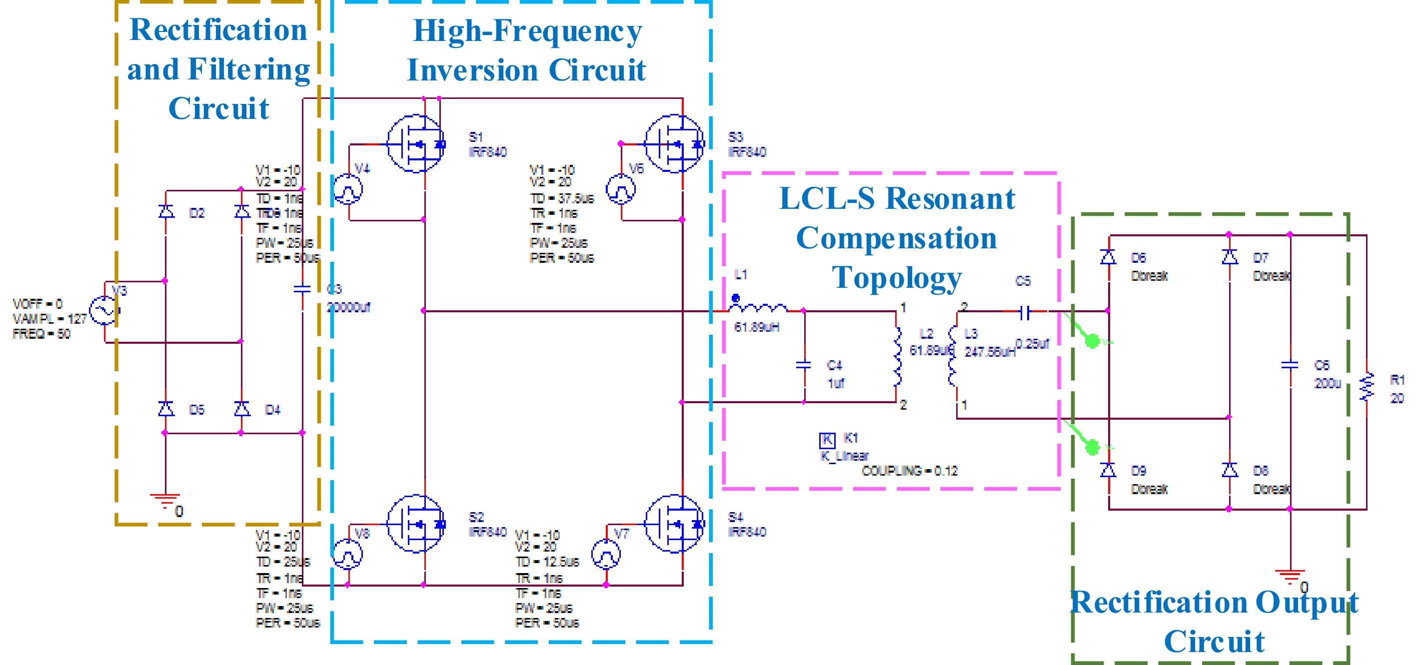
Figure 6.
Diagram of main circuit simulation.
According to the selection principle of filter capacitors in power supply design, the formula is:
$ C \geqslant \dfrac{{2.5T}}{R} $ (19) In this system, a filter capacitor C of 200 μF was chosen for the power rectification and filtering circuit. The rectified filtering effect is shown in Fig. 7.
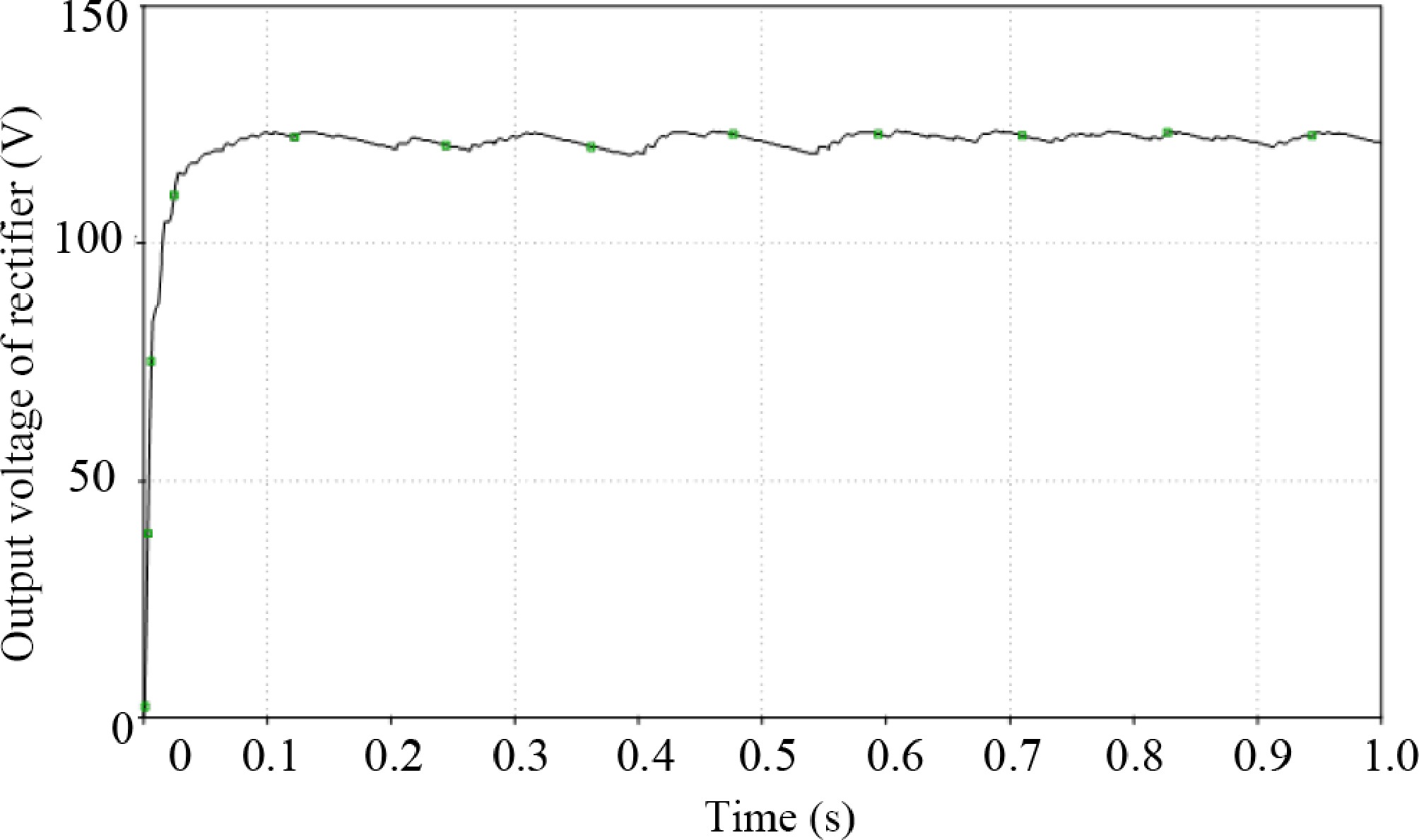
Figure 7.
Waveform of rectified output voltage.
The input voltage of the system reaches up to 127 V, while the output voltage needs to be only a few volts. Therefore, phase-shift control was chosen in the high-frequency inverter control method to reduce the output voltage at the backend, better meeting the system's output voltage requirements.
The high-frequency inverter circuit of the system uses MOSFET switches, controlled by a pulse source circuit, generating a control pulse as shown in Fig. 8. In the inverter circuit, switches S1 and S2 alternate conduction, and S3 and S4 alternate conduction, resulting in an alternating square wave voltage with a dead zone.
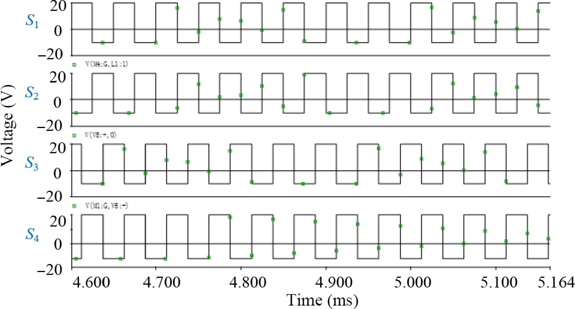
Figure 8.
Waveform of phase shift control pulse.
Figure 9 shows the output voltage waveform of the high-frequency inverter circuit.
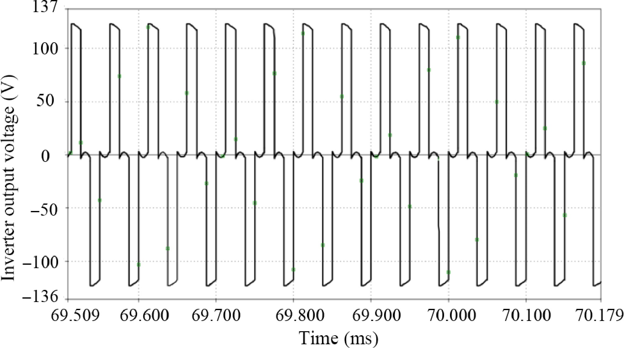
Figure 9.
Waveform of inverter circuit output.
For the LCL-S topology ICPT system, it can achieve primary constant current and secondary constant voltage characteristics, which is beneficial for achieving intrinsic safety. The primary current magnitude is only related to L1. In the design, L1 is determined based on the output power and wireless power transmission efficiency. The transmitting coil inductance Lp should be the same as L1 and resonate with the compensation capacitor Cp. For controlling the transmission power, the system uses the following parameters: La = Lp = 61.89 × 10⁻⁶ H, Ls = 247.56 × 10⁻⁶ H, and Cp = 1 × 10⁻⁶ F, Cs = 0.25 × 10⁻⁶ F.
The output voltage waveform of the main circuit is shown in Fig. 10. In the 0 to 20 ms range, the output voltage rises rapidly and then gradually stabilizes, eventually maintaining around 2 V. This waveform indicates that the system transitions quickly and steadily from the initial state to the steady state, with minimal voltage fluctuations in the steady state. The smooth curve demonstrates the system's good stability and reliability. This stable voltage output provides a foundation for further integration with the DC-DC converter and protection circuit to ensure an intrinsically safe output for electrical equipment in coal mines.
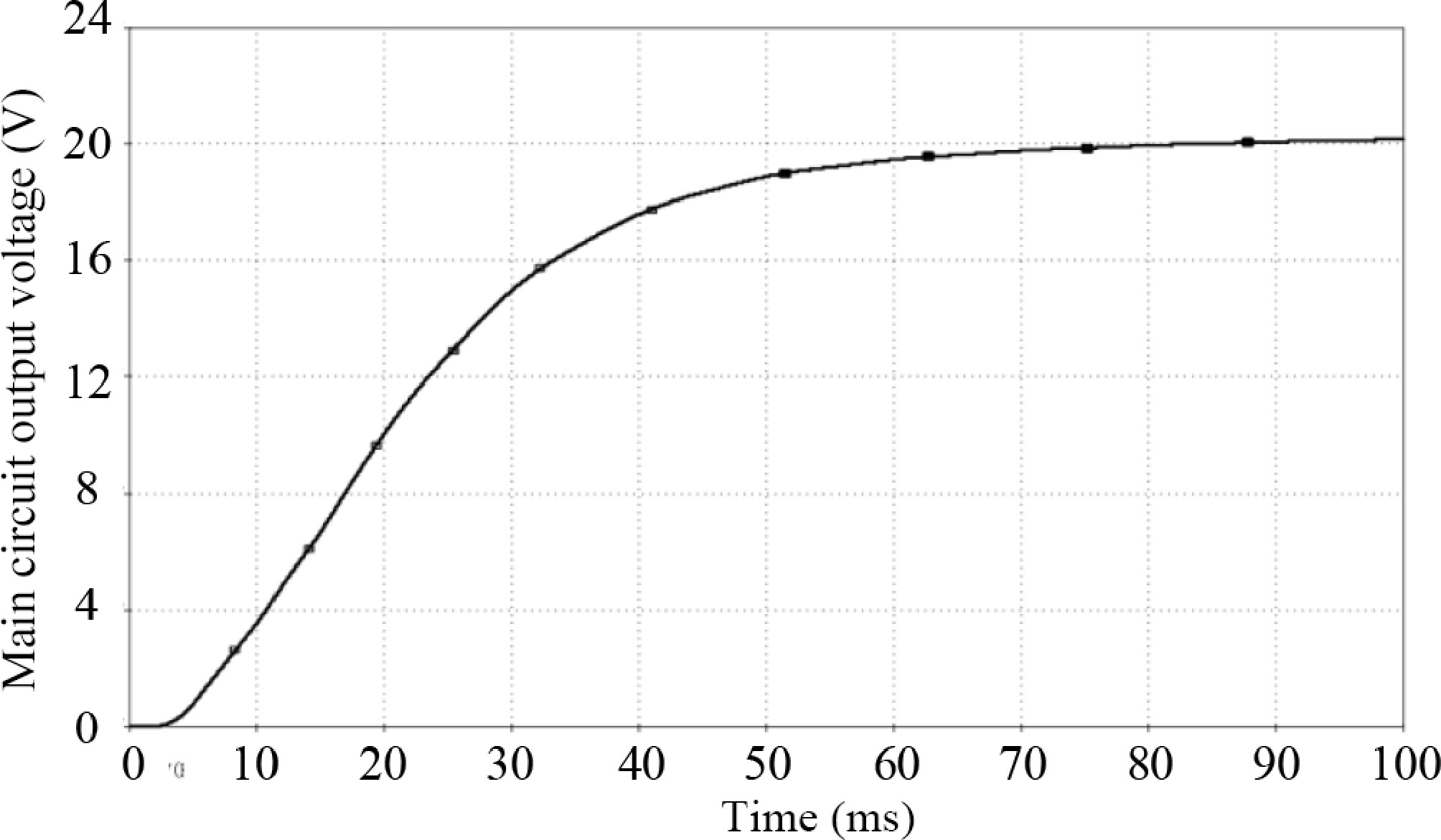
Figure 10.
Waveform of main circuit output.
As shown in Fig. 11, a CLC filter is incorporated at the input stage to enhance ripple suppression, extend capacitor lifespan, and improve system safety. The inclusion of this filter results in a smoother, sine-like input voltage waveform. To prevent a short circuit, a 0.01 Ω resistor was added in series with the pure inductor model in PSPICE. The parameters for the circuit are: a switching frequency of 20 kHz, and CLC filter parameters of C1 = 47 μF, C2 = 4.7 μF, and L3 = 1 mH. The simulation results are shown in Fig. 12.
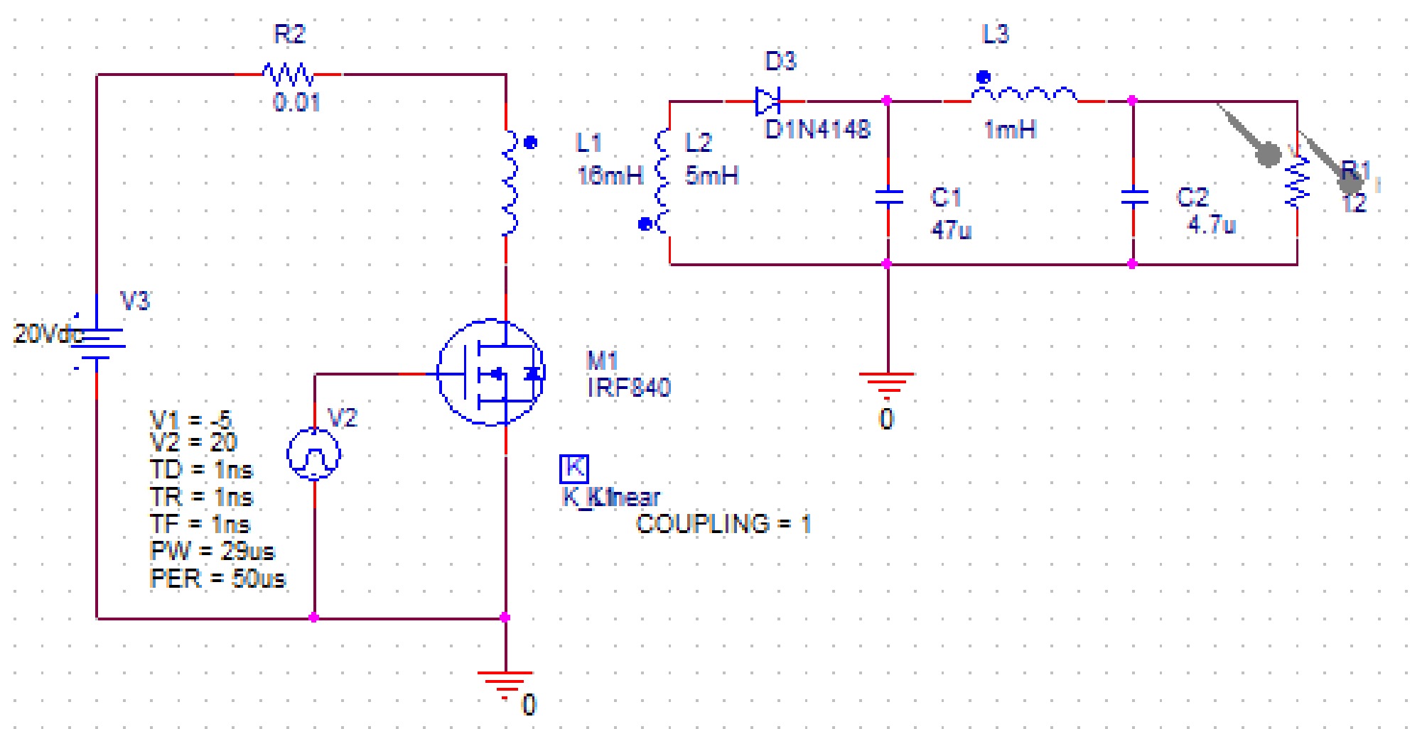
Figure 11.
Single-ended flyback DC-DC converter.
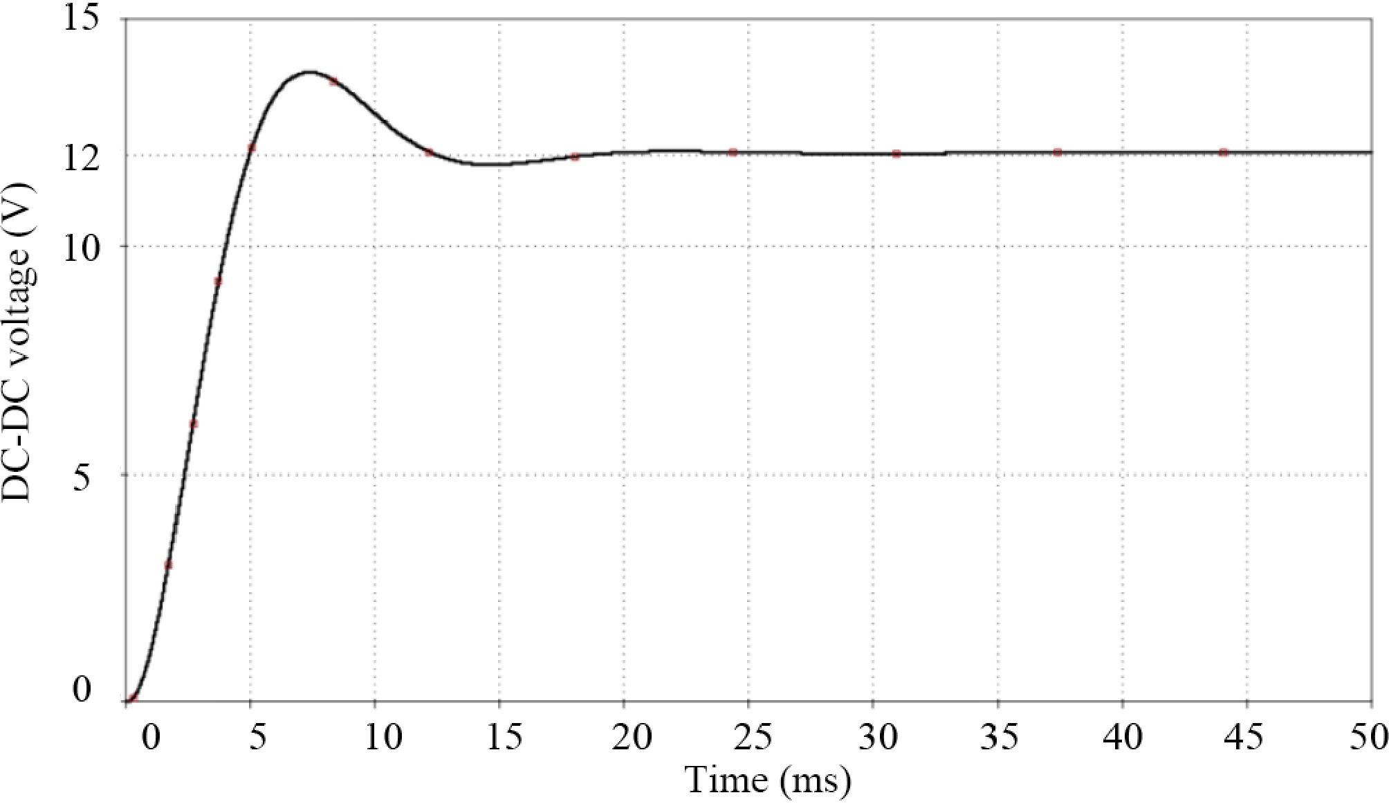
Figure 12.
Result of DC-DC voltage regulation simulation.
The waveform indicates that the voltage rises rapidly at the initial stage, reaching a peak of around 15 V at approximately 5 ms. The voltage then drops rapidly and, after a few minor oscillations, stabilizes around 12 V. From 14 ms onward, the voltage remains stable at about 12 V, with minimal fluctuation, demonstrating the system's ability to quickly adjust and maintain a stable output voltage. This simulation result verifies the effectiveness and fast response characteristics of the DC-DC converter in voltage regulation, ensuring stable voltage output under different load conditions.
Figure 13 shows the output voltage ripple, clearly indicating that the output ripple is less than 120 mV. The observed output voltage ripple, while slightly higher than conventional designs, is a direct result of prioritizing intrinsic safety in compliance with GB/T 3836.1-2021. This trade-off ensures robust operation in hazardous environments, with ripple levels well within the permissible range defined by the standard.
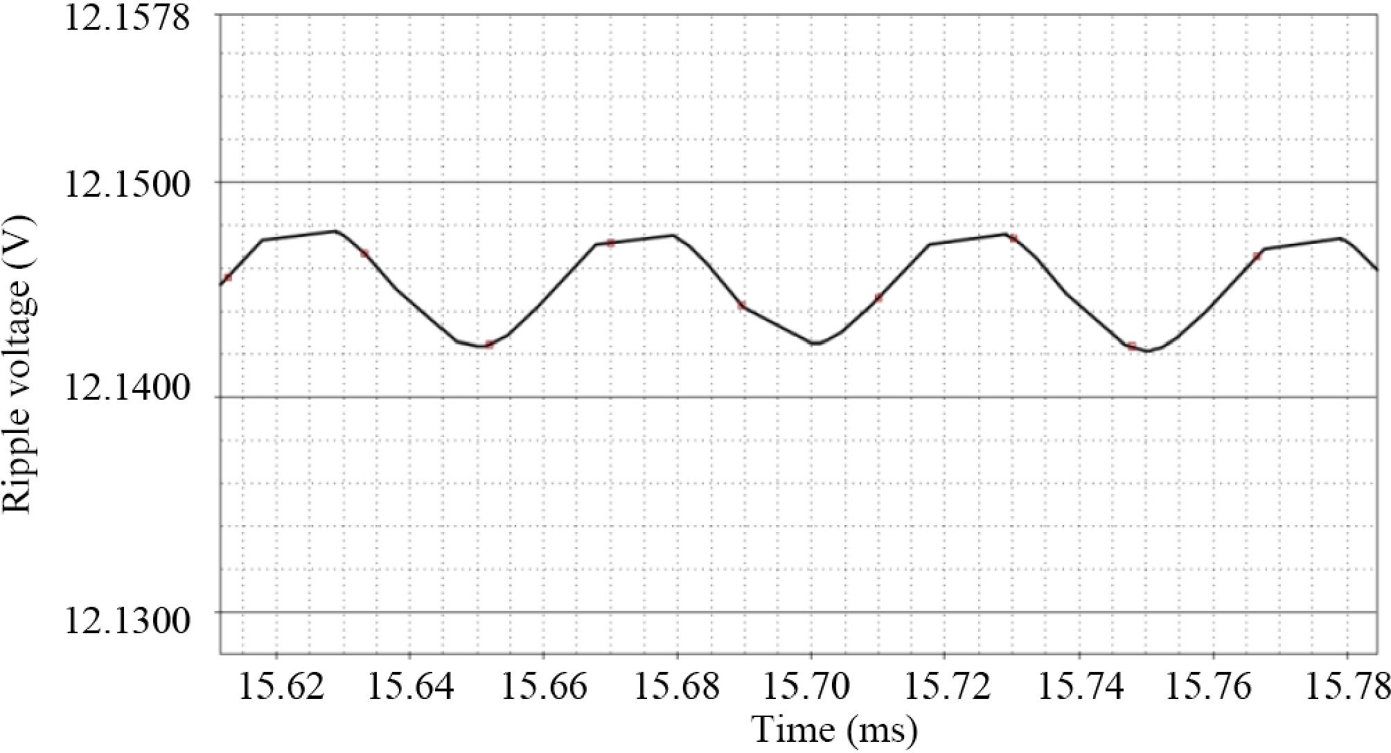
Figure 13.
Waveform of output voltage ripple.
Supplementary Figs S1 & S2 illustrate the simulation diagrams for the system's protection circuits. The first two comparators in the front end form the cutoff undervoltage and overvoltage protection circuits, while the subsequent comparator serves as the overcurrent protection comparator. The simulation results are shown in Fig. 14.
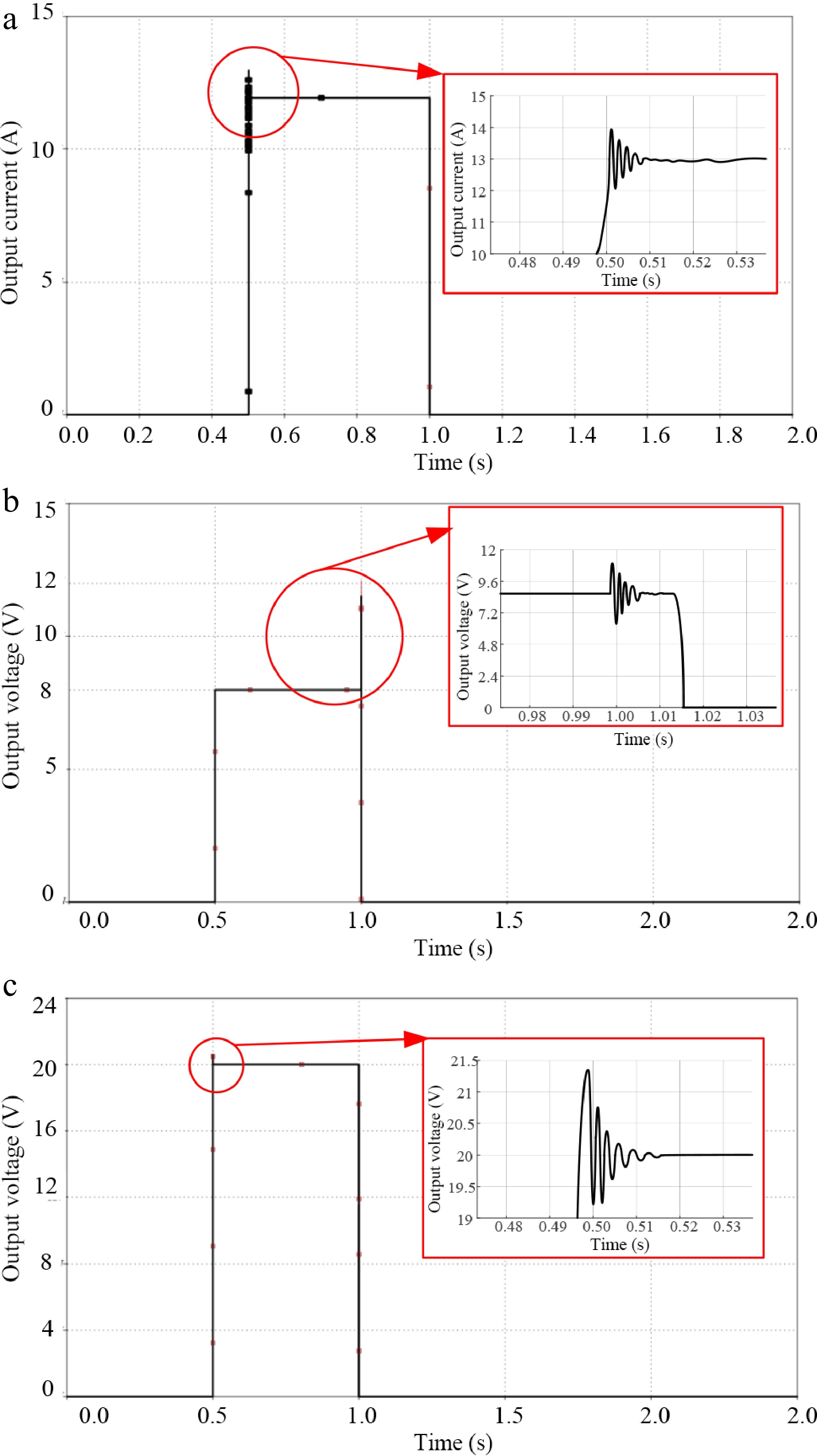
Figure 14.
Results of the protection circuit experiment. (a) Overcurrent protection simulation result. (b) Undervoltage protection simulation result. (c) Overvoltage protection simulation result.
When an overcurrent occurs, S2 immediately cuts off the protection circuit, and the circuit returns to normal once the overcurrent condition disappears. LM339-1 acts as the overvoltage comparator, and LM339-2 as the undervoltage comparator. If an overvoltage or undervoltage condition occurs, the comparator outputs a low level, causing S1 to disconnect the circuit. Multiple protection circuits, typically two or more, are set up to meet the need for multiple layers of protection. LM339-3 serves as the overcurrent comparator. When an overcurrent occurs, the voltage across sampling resistor R11 increases, causing the comparator's non-inverting input voltage to fall below the inverting input voltage, leading to a low-level output from the comparator. S2 then disconnects the circuit. Once the circuit returns to normal and the voltage across R11 drops below 0.7 V, the comparator's non-inverting input voltage exceeds the inverting input voltage, resulting in a high-level input and S2 reconnecting the circuit to resume normal output.
To clearly illustrate the dynamic response of the overcurrent protection circuit, magnified waveforms of the transient period are provided in Fig. 14a–c, showing the behavior before and after the protection is triggered.
Figure 14a demonstrates the system's response to an overcurrent condition. Initially, the current rises rapidly, exceeding the set overcurrent threshold, prompting the protection circuit to act immediately, cutting the current to zero. This indicates that the overcurrent protection circuit can quickly respond to and cut off the current to protect the system from damage.
Figure 14b shows the system's response to an undervoltage condition. Initially, the voltage is stable, but it then suddenly drops below the set undervoltage threshold. The protection circuit detects the undervoltage condition and quickly restores the voltage to a safe level, demonstrating the undervoltage protection circuit's effectiveness in monitoring and correcting low voltage situations to ensure normal system operation.
Figure 14c illustrates the system's response to an overvoltage condition. The initial voltage is low, but it quickly rises above the set overvoltage threshold. Upon detecting the overvoltage condition, the protection circuit immediately reduces the voltage to a safe level, effectively preventing damage to the system from excessive voltage and maintaining stable operation.
These three simulation waveforms verify the effectiveness of the protection circuits in different abnormal conditions, ensuring timely detection and response to overcurrent, undervoltage, and overvoltage situations to guarantee system safety and reliability.
Experimental verification
-
To verify the accuracy of the theoretical design, a prototype of the single-stage flyback converter employing the improved clamping-based protection circuit was constructed, as shown in Fig. 15.
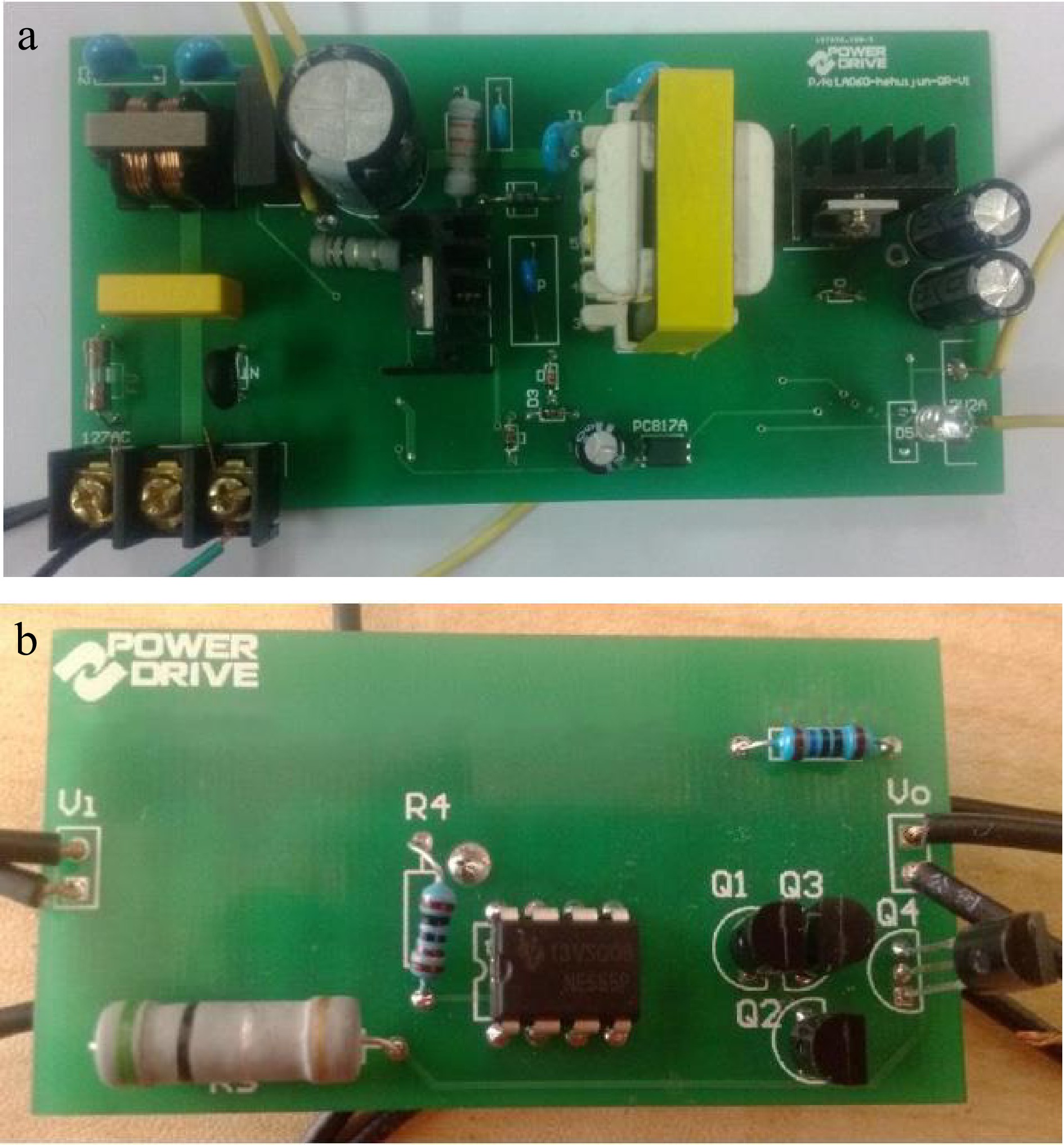
Figure 15.
Prototype of the improved clamping-based single-stage flyback converter. (a) Single-stage flyback converter. (b) Improved clamping-based protection circuit.
The intrinsically safe WPT system based on a single-ended flyback converter designed in this study has been constructed. Based on the comprehensive analysis above, in practical applications, the load operating time also needs to be considered. The diode selected for this system is the IN4007. The MOSFET chosen is the IRF840. The system's input ranges from 95 to 220 VAC at 50−60 Hz, and its output is 24 V/2 A. Based on the previous analysis, the experimental parameters are listed in Table 2.
Table 2. System parameter configuration table.
Parameter Value Parameter Value Vinmax 150 V R4 5 kΩ IBF 0.14 A R5 and R6 1 kΩ UDS 200 V R7 10 kΩ ID 6 A R8 1.3 kΩ Ui 20 V R9 3.3 kΩ Uo 12 V R10 1 kΩ Dmax 0.545 R11 0.7 kΩ R1 9.7 kΩ R12 10 kΩ R2 1 kΩ R13 1 kΩ R3 1.3 kΩ Cp 1 μF La and Lp 61.89 μH Cs 0.25 μF Ls 247.56 μH C1 47 μF L3 1 mH C2 4.7 μF C3 0.25 μF C4 200 μF The input voltage and current waveforms during system operation are shown in Fig. 16, where the blue line represents the input voltage waveform and the purple line represents the input current waveform. The current waveform closely follows the voltage waveform, essentially meeting the design requirements. Figure 17 shows the gate voltage of the main switching transistor and the zero-crossing detection terminal waveform. From the figure, it can be seen that the system's off-time is 8 µs, which is consistent with the practical application background in coal mines.
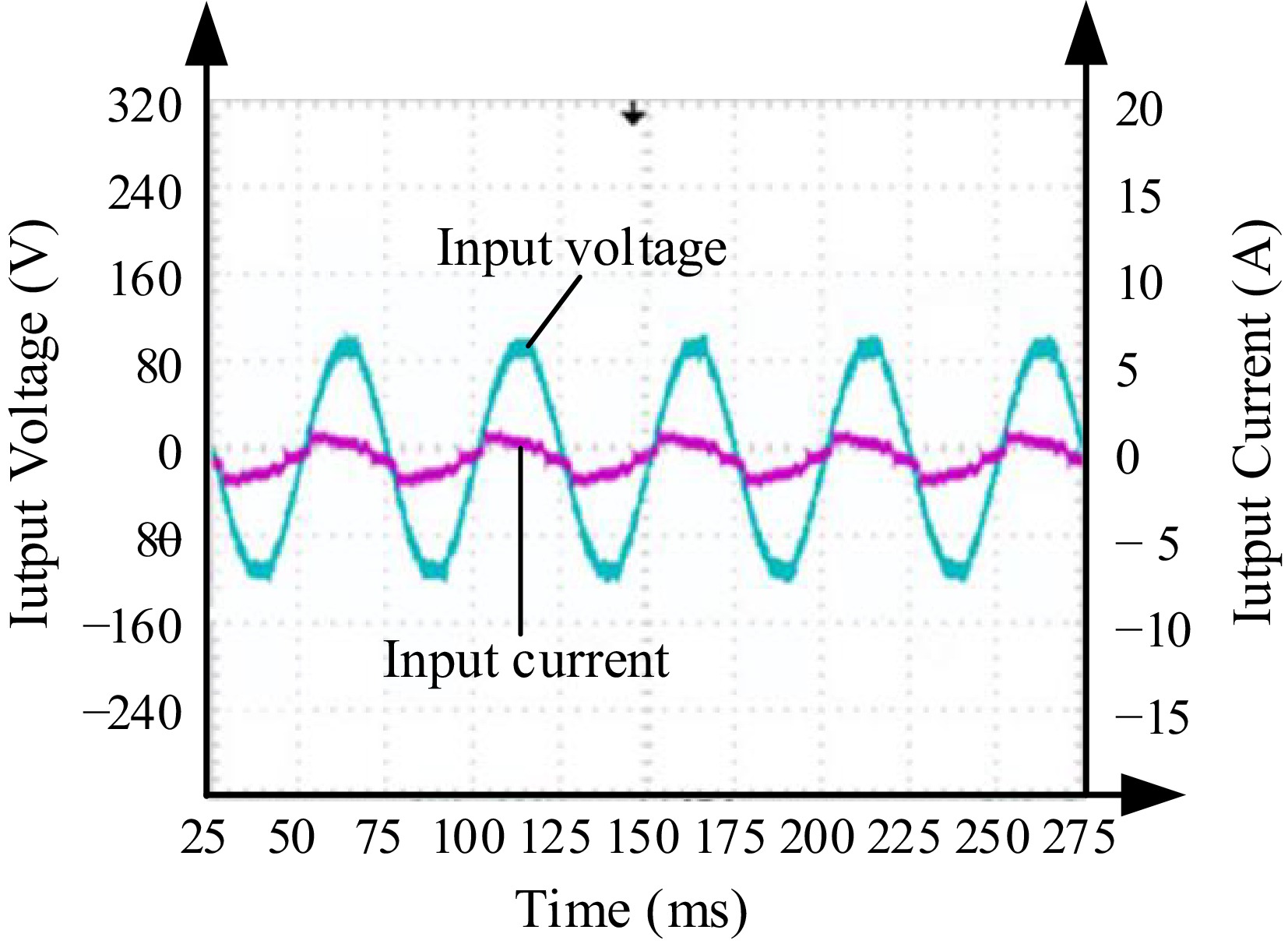
Figure 16.
Waveform of the input voltage and current.
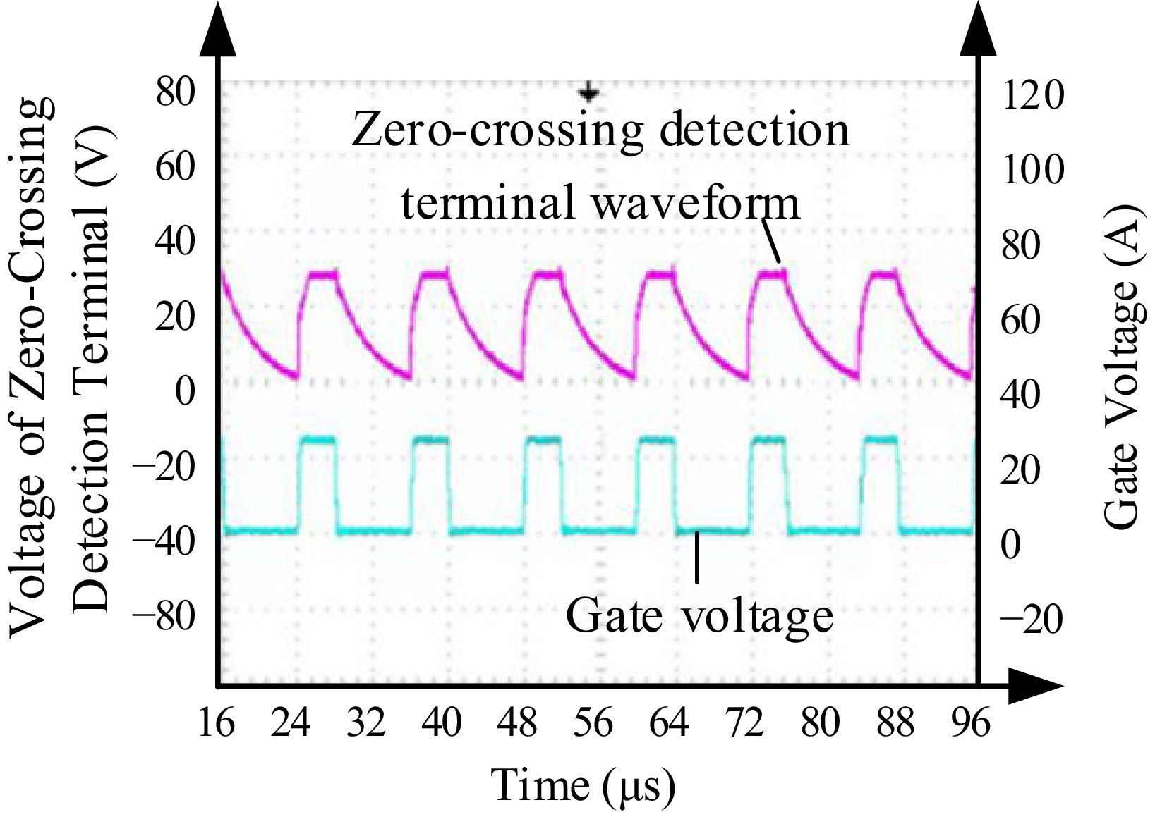
Figure 17.
Waveform of the gate voltage and the zero-crossing detection terminal.
Figure 18 shows the inverter control voltage and the primary current of the WPT system. The control voltage exhibits pulse signals, while the primary current is a smooth AC signal, indicating effective driving by the inverter. The time axis in microseconds demonstrates high-frequency operation. The primary current ranges from 0 to 1.4 A, and the control voltage from −8 to 24 V. These waveforms confirm efficient and stable system performance. The primary current closely follows the control voltage, showcasing excellent dynamic response.
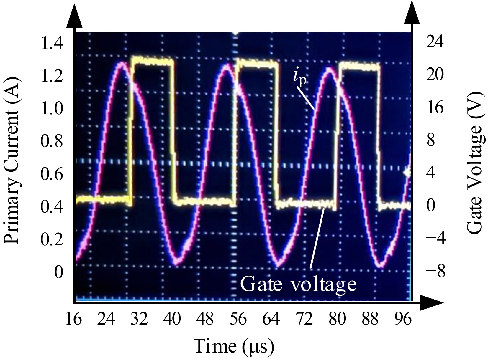
Figure 18.
Waveform of inverter control voltage and WPT system primary current.
As shown in Fig. 19, the system's output voltage waveform can achieve the design requirement of 24 V output. However, the output voltage ripple is relatively large. This can be improved by adding a filter capacitor at the output. However, increasing the output filter capacitor may result in the system output not being intrinsically safe, which would contradict the original design intention. Therefore, such a power supply is suitable for intrinsically safe equipment where the voltage quality requirement is not too stringent.
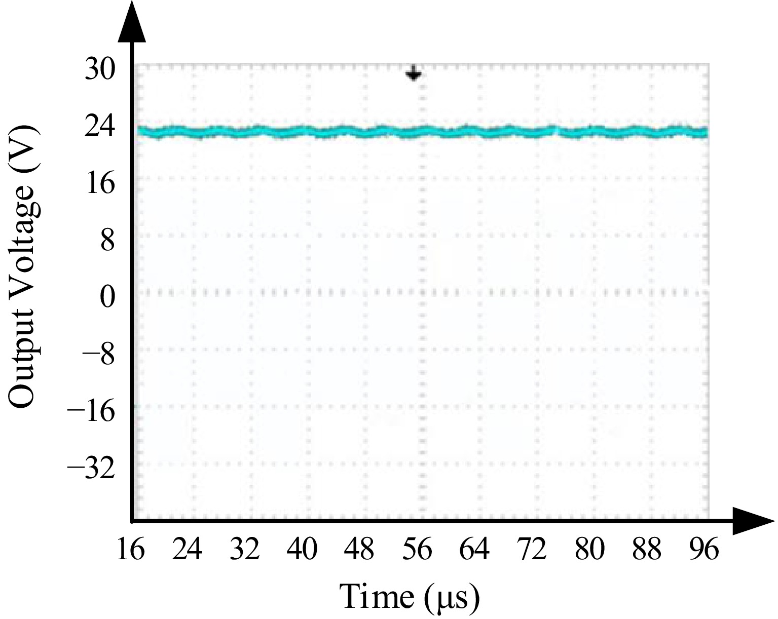
Figure 19.
Waveform of the output voltage.
Figure 20 shows the actual experimental waveform of the improved cutoff protection circuit presented in this paper. The delay time for the protection circuit's switch device to act is about 5 μs, enabling rapid circuit disconnection. Compared with ordinary cutoff protection circuits, this circuit has significantly lower spark power, approximately 44 W, which is one-twelfth of that of ordinary cutoff protection circuits. This greatly reduces the spark discharge energy under the same cutoff time. Therefore, this protection effectively enhances the output power of intrinsically safe power supplies. To some extent, this protection circuit disconnects the influence of the power potential on the spark discharge current. The circuit output meets the requirements of intrinsic safety and non-explosion evaluation, making the circuit intrinsically safe.
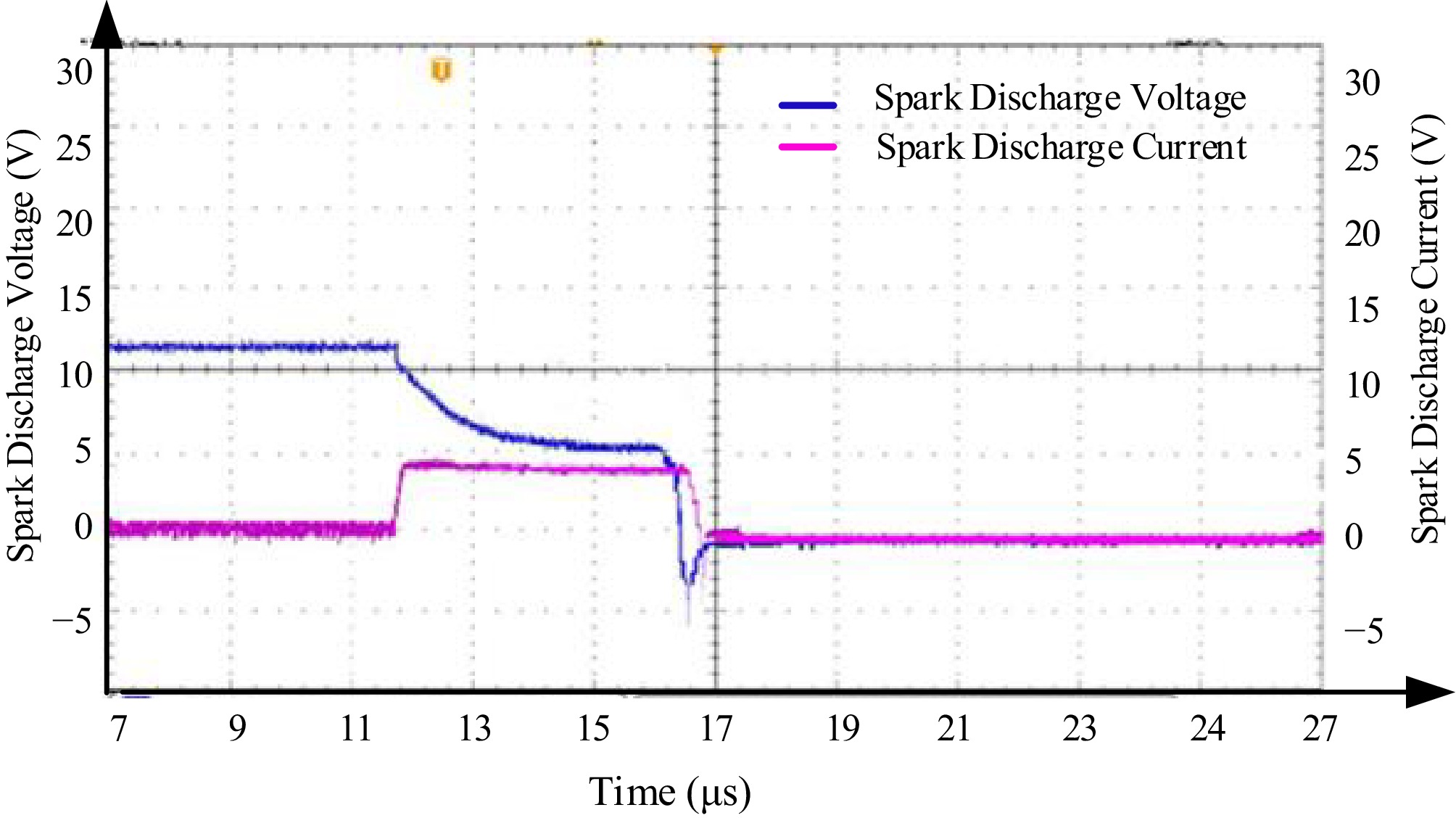
Figure 20.
The waveform of the ameliorated cutoff experiment.
Verification of the intrinsically safe performance of the DC-DC circuit
-
The system uses minimum ignition curves and theoretical derivations to verify whether the DC-DC voltage regulation meets intrinsic safety standards.
The allowable short-circuit current for equipment under a voltage level of 17 V, considering a 1.5 times safety margin, is 2,320 mA. The maximum output current of this system is 1 A, meeting national standards.
When spark discharge occurs in the circuit, the experimental curve of the relationship between the capacitance of the switching converter and the average duration of capacitor short-circuit spark discharge is used as the calculation standard. During spark discharge, if the filter capacitor is 40 μF, the discharge duration TC is 300 μs. The intrinsic safety cutoff protection achieves a response speed of 5 μs. Assuming no protective action during spark discharge, the secondary side of the transformer is discharging with a secondary current of 1 A. According to GB/T 3836.4-2010 and IEC 60079-11:2011, the allowable maximum capacitance Cmax under 17 V in IIB explosive environments can be calculated by Cmax = 2E/(U)2, where E is the maximum permissible ignition energy (typically 85 µJ for IIB gases) and U is 17 V. Calculated Cmax = 590 μF. Considering a 1.5× safety margin, the safe capacitance limit becomes approximately 393 μF. Therefore, the equivalent capacitance of 57 μF is significantly below this threshold, ensuring intrinsic safety. Furthermore, the system's equivalent value of 57 μF remains well within this safe operating region.
Therefore, based on theoretical analysis, the DC-DC converter circuit meets intrinsic safety requirements.
Under the rated input condition of 286.37 W, the proposed system delivers a measured output power of 241.89 W, achieving a power transfer efficiency of 84.47%. These results verify the effectiveness of the designed single-stage flyback converter and the improved clamping-based protection circuit.
Comparative analysis
-
As shown in Table 3, this section presents a detailed comparative analysis between the proposed intrinsically safe wireless power transfer system for underground mining and the findings from three other studies.
Table 3. Comparison between WPT system and other mining power systems.
Technology Safety and reliability Output of voltage and power Ref. Laser power converters (LPC) Emphasis on efficiency and safe conversion technology Conversion efficiency: 33.8%, laser power input: 1 mW [17] Hybrid front-end converters, ultracapacitors, sodium-based batteries Ensures reliable operation and harmonic reduction Energy storage capacity: 3 MJ, peak power: 24 MW, load cycle: 10–60 s [18] Single-ended flyback converters, voltage regulation, protection circuits Intrinsically safe design, rapid response to anomalies Output voltage: 12 V, ripple: < 120 mV, protection response: 5 µs This article The proposed intrinsically safe WPT system demonstrates significant advantages in terms of safety, efficiency, and applicability to underground coal mining compared to the other studies. It ensures stable and safe power delivery in hazardous environments, which is critical for mining operations. The detailed analysis and comparison highlight the unique strengths and innovative aspects of the system, making it a valuable contribution to mining technology.
-
This study aims to design and validate an intrinsically safe wireless power transfer system for underground coal mine environments. The detailed design and implementation of core components, including the single-ended flyback converter, voltage regulation circuits, and protection circuits, are presented. The system's performance and safety have been verified through simulation and actual measurements. An undervoltage and overvoltage protection circuit based on the LM339 comparator is proposed. Combined with the CLC filter circuit, it extends the capacitor's lifespan, effectively reduces the impact of power voltage fluctuations on the system, and ensures stable operation. The optimized single-ended flyback converter meets intrinsic safety requirements while ensuring efficiency. Comparative analysis shows that with a voltage of 17 V and considering a 1.5 times safety margin, the system's equivalent capacitance is only 57 μF, meeting intrinsic safety requirements with a significant safety margin. Additionally, the intrinsic safety cutoff protection has a response speed of 5 μs. Experimental results indicate that the protection circuit can respond quickly in abnormal situations, ensuring system safety.
In this study, the designed system achieves an output power of approximately 242 W, which meets the requirements of current intrinsically safe underground devices such as gas sensors, communication systems, lighting, and monitoring equipment in coal mines. For scenarios requiring higher power outputs, potential constraints imposed by intrinsic safety standards have been analyzed, and possible solutions as well as future research directions are discussed to further expand the system's applicability.
However, this study primarily focuses on the design of voltage regulation and protection circuits, without delving into other factors that may affect system performance, such as temperature, humidity, and vibration. While the protection circuit design features fast response and low power consumption, its long-term operational stability and maintenance needs are not discussed in detail. Due to the constraints of the current experimental setup, the harsh conditions typical of underground coal mines could not be simulated, and comprehensive testing in simulated environments and long-term durability assessments were not conducted. Therefore, a limitation of this work is the potential discrepancy between the simulated conditions and real-world explosive atmospheres. Nonetheless, future work will incorporate prototype-level experiments in certified testing facilities to validate these findings.
This research was funded by the 2020 Anhui Provincial Natural Science Foundation Energy Internet Joint Fund Project (Grant No. 2008085 UD14).
-
The authors confirm their contributions to the paper as follows: study conception and design: Zheng K, Zhang L; data collection: Zhang C, Zhang L; analysis and interpretation of results: Zheng K, Wang X; draft manuscript preparation: Wang X. All authors reviewed the results and approved the final version of the manuscript.
-
Data sharing not applicable to this article as no datasets were generated or analyzed during the current study.
-
The authors declare that they have no conflict of interest.
- Supplementary Fig. S1 Diagram of overcurrent protection circuit simulation.
- Supplementary Fig. S2 Diagram of undervoltage and overvoltage protection circuit simulation.
- Copyright: © 2025 by the author(s). Published by Maximum Academic Press, Fayetteville, GA. This article is an open access article distributed under Creative Commons Attribution License (CC BY 4.0), visit https://creativecommons.org/licenses/by/4.0/.
-
About this article
Cite this article
Zhang L, Zhang C, Wang X, Zheng K. 2025. Intrinsically safe wireless power transfer system based on single-ended flyback converter. Wireless Power Transfer 12: e030 doi: 10.48130/wpt-0025-0027 

Intrinsically safe wireless power transfer system based on single-ended flyback converter
- Received: 13 May 2025
- Revised: 17 June 2025
- Accepted: 21 July 2025
- Published online: 26 November 2025
Abstract: In underground coal mines, the intrinsic safety of electrical equipment is crucial due to frequent voltage fluctuations that can damage electronic devices and compromise system reliability and safety. This study aims to design an intrinsically safe wireless power transfer system using a single-ended flyback converter. The system incorporates an LCL-S resonant compensation topology, undervoltage and overvoltage protection circuits based on the LM339 comparator, and a CLC filter circuit to enhance capacitor life and system stability. Experimental results indicate that with an input voltage of 17 V and a safety margin of 1.5 times, the system's equivalent capacitance can reach up to 110 μF, while the actual capacitance is 57 μF, confirming that the DC-DC converter meets intrinsic safety requirements. The protection circuits for overcurrent, undervoltage, and overvoltage respond swiftly to abnormal conditions, ensuring system safety. These circuits offer rapid response and low power consumption, while the CLC filter circuit significantly extends capacitor life, enhancing overall system stability and safety. It is important to note that the experiments were conducted under controlled laboratory conditions, focusing on electrical stability rather than explosive environments, as current laboratory facilities do not support explosive atmosphere simulations.