


-
With the rapid development of industrial fields[1,2] such as consumer electronics, drones, robotics, electric vehicles, medical equipment, and bionic robotic dogs, smart mobile devices are being widely used in complex scenarios like disaster rescue, field exploration, and underwater wireless power transmission[3−6]. In wireless power transfer (WPT) systems, the series–series (SS) compensation topology enables contactless energy transmission by eliminating the need for physical connectors. This feature significantly improves system reliability and durability by mitigating issues caused by corrosion, dust, and moisture in harsh environments[7]. Additionally, the SS topology is structurally simple, allowing for the integration of the resonant capacitor and power converter onto a single PCB, which contributes to lightweight design and enhances power density—two critical factors in portable and space-constrained applications. Owing to these advantages, SS compensation networks have been widely adopted in various low- and mid-power WPT applications, including mobile robots, unmanned aerial vehicles (UAVs), smartphones, power banks, medical devices, and other consumer electronic products[8−10]. Moreover, the simplicity of the SS configuration also facilitates ease of control and design scalability, making it a practical choice for both research prototypes and commercial implementations.
However, their ability to operate continuously faces significant challenges in power supply. As a result, bidirectional wireless power transfer (BWPT) has been rapidly advancing in these fields[11,12]. In BWPT systems, compensation networks are typically chosen based on their suitability for bidirectional energy flow. Current-source-type compensation topologies are preferred, such as SS compensation, double-side LCC, and double-side LCL[13−18]. To maintain stable power transfer, it is essential to keep the primary and secondary converters phase-synchronized. However, with the trend toward higher frequencies and increased power density, especially in megahertz frequency-level systems driven by GaN devices, phase synchronization techniques face stringent requirements. Loss of synchronization signals can lead to increased power losses, reduced efficiency, loss of soft switching, zero voltage switching (ZVS), and even potential damage to power devices. These issues significantly affect the stability and practicality of BWPT systems.
In the application of BWPT, there is no direct-wired communication between the converters on both sides, making direct phase synchronization challenging[19]. Traditionally, current transformers have been used to synchronize the phase signals of the converters to provide synchronization signals to the secondary-side converter[20]. A method was employed to achieve synchronous rectification (SR) through a radio frequency (RF) wireless communication interface. However, due to the relatively high operating frequency of the converters and the inherent transmission delays in real-time communication, combined with the susceptibility of RF communication to electromagnetic interference, this method lacks sufficient stability. In a novel 16-ary pulse interval modulation simultaneous wireless power and data transfer scheme, based on a SS compensation topology, was proposed[21]. Through this integrated power and data transmission method, the synchronization signal is transferred from the primary side to the secondary side, thereby enabling synchronous rectification. An inductive phase synchronization method, using an auxiliary winding, is proposed[22]. This approach transmits synchronization signals based on the voltage across the auxiliary winding and the current through the magnetic coupling's secondary winding. However, it imposes strict electromagnetic compatibility requirements on the winding and is highly susceptible to interference, which can compromise system stability.
This paper presents a phase synchronization method for SR in BIPT systems that eliminates the need for communication links, sensors, or auxiliary windings, effectively addressing the demand for high-speed synchronization. The method samples the voltage across the secondary compensation capacitor in the SS compensation network. After filtering and voltage division, the signal is fed into a high-speed comparator. The comparator generates a pulse signal, which is sent to the microcontroller unit (MCU). The MCU processes this signal, adjusts the phase and dead time, and controls the secondary-side switches to achieve SR. In contrast to traditional approaches, this method does not depend on current transformers, RF communication, or auxiliary coils, making it more resistant to electromagnetic interference. The proposed solution offers high stability, low cost, strong reliability, and high efficiency. Compared to integrated SR chips, the proposed scheme exhibits more stable and efficient operation under high-frequency conditions, while also enabling output power regulation.
-
A typical BWPT system is illustrated in Fig. 1. In this configuration, two bidirectional converters—one on the primary side and one on the secondary side—control the power flow. BWPT is achieved through coil coupling combined with its compensation network. It shows a common application of the full-bridge circuit within a BIPT system. In this circuit, switches Q1–Q4 serve as the control switches for the primary-side full-bridge inverter, while switches Q5–Q8 control the secondary-side full-bridge rectifier. Lp and Ls represent the self-inductance of the primary and secondary coupling coils, respectively, with M denoting their mutual inductance. Uin and Uout are input voltage and output voltage; U1 and U2 are the voltages generated by the full-bridge inverter on the primary side and the full-bridge rectifier on the secondary side, respectively; and I1 and I2 are the corresponding AC currents on the primary and secondary sides. The primary and secondary sides are designed with hardware to capture frequency and phase signals. Under MCU processing, phase shifting and dead time settings are applied to achieve SR during power transmission.
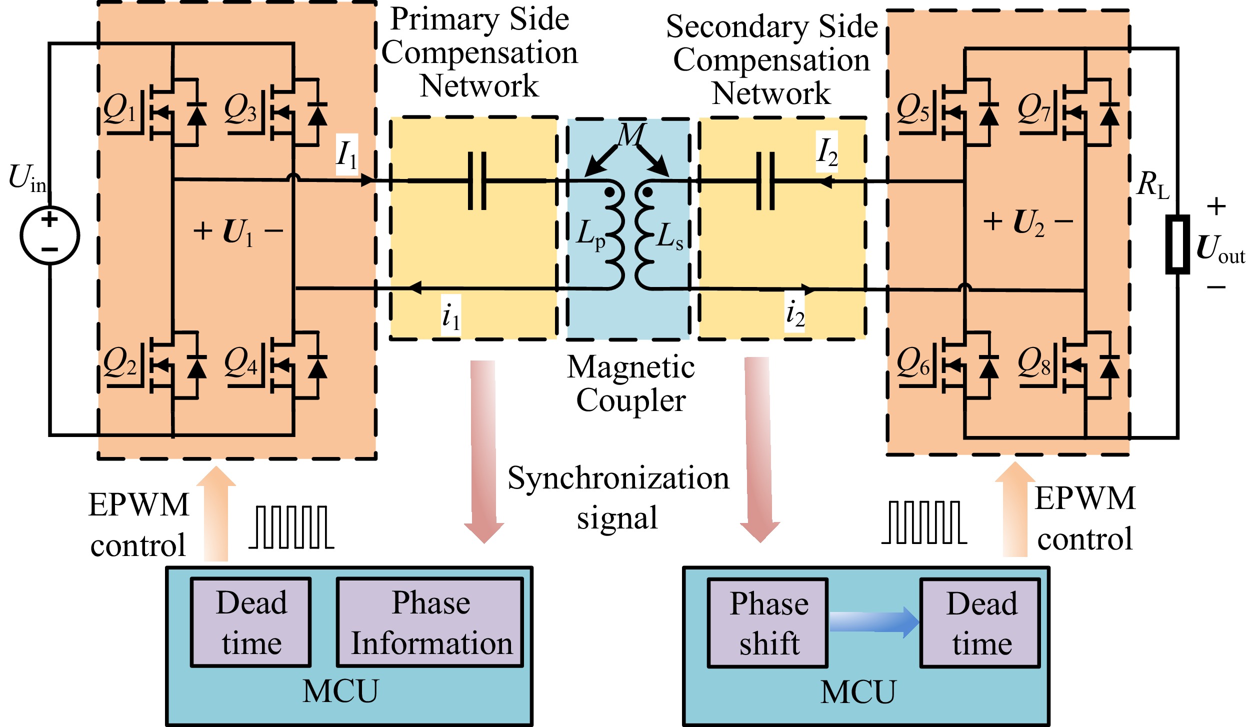
Figure 1.
A typical structure block diagram of the BWPT system.
Analysis of the circuit based on SS compensation
-
The approach employed in this paper involves sampling at the zero crossing points of the compensation capacitors within the SS compensation network of the secondary side compensation. As illustrated in Fig. 2, this WPT topology features Lp and Ls, which denote the self-inductances of the primary and secondary magnetic coupling coils, respectively; Rp and Rs, which represent the internal resistances on the primary and secondary sides; Cp and Cs are the compensation capacitors on both sides; RL represents the DC constant load resistance in the BWPT system, while Req denotes the equivalent AC resistance. The following calculations detail the parameters of the S–S compensation network as[22]:
$ \left\{ {\begin{array}{*{20}{l}} {{L_p}{C_p} = \dfrac{1}{{{\omega ^2}}} = \dfrac{1}{{{{(2\pi {f_{SW}})}^2}}}} \\ {{L_s}{C_s} = \dfrac{1}{{{\omega ^2}}} = \dfrac{1}{{{{(2\pi {f_{SW}})}^2}}}} \end{array}} \right. $ (1) where, fs and ω represent the switching frequency, and the angular switching frequency, respectively.

Figure 2.
Equivalent circuit of the BWPT system.
Thus, the primary-side reactance is denoted as Xp, and the secondary-side reactance as XS:
$ \left\{ {\begin{array}{*{20}{l}} {{X_p} = \omega {L_p} - \dfrac{1}{{\omega {C_p}}}} \\ {{X_S} = \omega {L_s} - \dfrac{1}{{\omega {C_s}}}} \end{array}} \right. $ (2) The equivalent impedances of the primary, secondary sides, and the equivalent resistance Req of the rectifier are[22]:
$ \left\{ {\begin{array}{*{20}{l}} {{Z_p} = {R_p} + j{X_p}} \\ {{Z_s} = {R_s} + j{X_p}} \\ {{R_{eq}} = 8{\pi ^{ - 2}}{R_L}} \end{array}} \right. $ (3) In the resonant state, the currents of the primary and secondary sides can be obtained by combining Eqs (1) and (2) respectively:
$ \left\{ {\begin{array}{*{20}{l}} {{{\dot I}_1} = \dfrac{{{{\dot U}_1}({R_{eq}} + {Z_s})}}{{{Z_p}({R_{eq}} + {Z_s}) + {{(\omega M)}^2}}}} \\ {{{\dot I}_2} = \dfrac{{j\omega M{{\dot U}_1}}}{{{Z_p}({R_{eq}} + {Z_s}) + {{(\omega M)}^2}}}} \end{array}} \right. $ (4) Based on Eq. (4) and Req, the system output voltage U2 is:
$ {\dot U_2} = {\dot I_2}{R_{eq}} = \dfrac{{j\omega M{R_{eq}}{{\dot U}_1}}}{{{Z_p}({R_{eq}} + {Z_s}) + {{(\omega M)}^2}}} $ (5) And based on the input voltage Uin and current I1, the input impedance Zin and angle θin are:
$ \left\{ {\begin{array}{*{20}{l}} {{Z_{in}} = \dfrac{{{{\dot U}_1}}}{{{{\dot I}_1}}} = \dfrac{{{Z_p}({R_{eq}} + {Z_s}) + {{(\omega M)}^2}}}{{({R_{eq}} + {Z_s})}}} \\ {{\theta _{in}} = {{\tan }^{ - 1}}\left(\dfrac{{{\text{Im}}[{Z_{in}}]}}{{{\rm Re} [{Z_{in}}]}}\right)} \end{array}} \right. $ (6) According to Kirchhoff's laws, the output impedance Zout, and its phase angle can θout be expressed as:
$ \left\{ {\begin{array}{*{20}{l}} {{Z_{out}} = {Z_p} + \dfrac{{{{(\omega M)}^2}}}{{{R_{eq}}}}} \\ {{\theta _{out}} = {{\tan }^{ - 1}}\left(\dfrac{{{\rm Im} [{Z_{out}}]}}{{{\rm Re} [{Z_{out}}]}}\right)} \end{array}} \right. $ (7) Based on Fig. 2 and Kirchhoff's laws, the ground-referenced voltages across the resonant capacitor on the secondary side can be derived as Ucs1 and Ucs2, which are expressed as:
$ \left\{ {\begin{array}{*{20}{l}} {{{\dot U}_{cs1}} = - j\omega M{{\dot I}_1}} \\ {{{\dot U}_{cs2}} = - j\omega M{{\dot I}_1} - \dfrac{1}{{j\omega {C_s}}}{{\dot I}_2}} \end{array}} \right. $ (8) Thus, the voltage difference across the secondary-side resonant capacitors, denoted as Ucs, can be expressed as:
$ {\dot U_{cs}} = {\dot U_{cs2}} - {\dot U_{cs1}} = - \dfrac{{M{{\dot U}_1}}}{{({Z_p}({R_{eq}} + {Z_s}) + {{(\omega M)}^2}){C_s}}} $ (9) Based on the input voltage Uin and the current expression in Eq. (4), the input power Pin and output power Pout can be derived as follows:
$ \left\{ {\begin{array}{*{20}{l}} {{P_{in}} = {\rm Re} ({U_{in}}{{\tilde I}_1}) = \dfrac{{U_{in}^2({R_{eq}} + {R_s})}}{{{R_p}({R_{eq}} + {R_s}) + {{(\omega M)}^2}}}} \\ {{P_{out}} = \dfrac{{{{(\omega M)}^2}{R_{eq}}U_{in}^2}}{{{{({R_p}({R_{eq}} + {R_s}) + {{(\omega M)}^2})}^2}}}} \end{array}} \right. $ (10) And the system's output efficiency η can be expressed as:
$ \eta = \dfrac{{{P_{out}}}}{{{P_{in}}}} = \dfrac{{{{(\omega M)}^2}{R_{eq}}}}{{({R_{eq}} + {R_s})[{R_p}({R_{eq}} + {R_s}) + {{(\omega M)}^2}]}} $ (11) For the SS compensation network, output power Pout can be regulated using phase-shift modulation (PSM). Based on Fig. 3, there exists a 90° phase difference between I1 and I2 when the circuit operates under resonant conditions[23,24]. The switching waveforms of the inverter and the rectifier, along with I1, I2, U1, and U2, are illustrated in Fig. 3. When the PSM technique is applied to both the inverter and rectifier stages, the band-pass filtering property of the resonant compensation network allows for the use of the fundamental harmonic approximation to estimate the RMS values of U1 and U2. Consequently, the following expression can be derived[24]:
$ \left\{ \begin{gathered} {U_1} = \dfrac{{2\sqrt {\cos (\alpha ) + 1} }}{\pi }{U_{in}} \\ {U_2} = \dfrac{{2\sqrt {\cos (\beta ) + 1} }}{\pi }{U_{out}} \\ \end{gathered} \right. $ (12) Therefore, power regulation can be realized by adjusting the output voltage Uout accordingly.
$ {U_{out}} = \dfrac{\pi }{{2\sqrt {\cos (\beta ) + 1} }}{U_2} $ (13) 
Figure 3.
Phase-shift modulation-based power control strategy for the S–S compensation topology.
-
Since Ucs1 and Ucs2 have high voltages in the compensation network, and Ucs2 is connected to the rectifier with a square wave voltage waveform, they cannot be directly fed into the comparator. Based on the characteristics of capacitors:
$ \left\{ {\begin{array}{*{20}{l}} {di = C\dfrac{{du}}{{dt}}} \\ {{Z_c} = \dfrac{1}{{j\omega C}}} \end{array}} \right. $ (14) It is known that the voltage across a capacitor cannot change abruptly, making it suitable for stable voltage sampling. As shown in Fig. 4, this approach uses two capacitors, C1 and C2, to filter out common-mode signals from Ucs1 and Ucs2. Then, voltage divider resistors R1 and R2 are used to obtain the ground-referenced voltages U1 and U2. These signals are then fed into a comparator, which generates a pulse signal for the MCU. Upon receiving the synchronization signal, the MCU applies phase shifting, and dead time control to the gate signals of Q5–Q8.
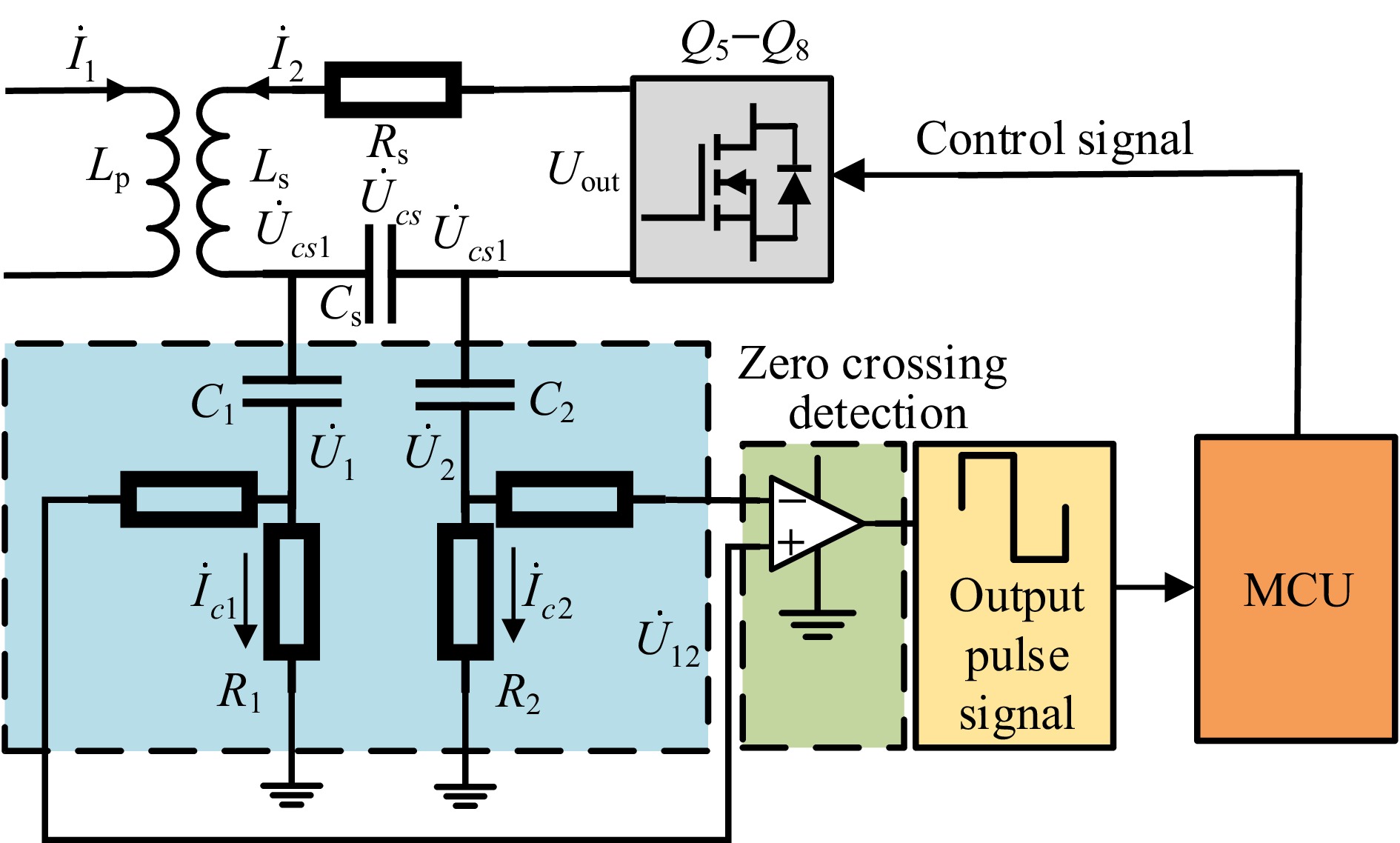
Figure 4.
Diagram of the circuit of the zero-crossing detection.
Due to the presence of the voltage divider resistors, the currents Ic1 and Ic2 are very small, only a few milliamps, and can be neglected in I2. In Eqs (5) and (6), Ucs1 and Ucs2 have already been derived, and the ground-referenced branch resistance of Ucs1 and Ucs2 is given by:
$ \left\{ {\begin{array}{*{20}{l}} {{Z_1} = \dfrac{1}{{j\omega {C_1}}} + {R_1}} \\ {{Z_2} = \dfrac{1}{{j\omega {C_2}}} + {R_2}} \end{array}} \right. $ (15) From Eq. (13), the sampled voltages U1 and U2 obtained by the high-speed comparator can be expressed as:
$ \left\{ {\begin{array}{*{20}{l}} {{{\dot U}_1} = {{\dot U}_{cs1}}\dfrac{{j\omega {C_1}{R_1}}}{{1 + j\omega {C_1}{R_1}}}} \\ {{{\dot U}_2} = {{\dot U}_{cs2}}\dfrac{{j\omega {C_2}{R_2}}}{{1 + j\omega {C_2}{R_2}}}} \end{array}} \right. $ (16) Equations (5) and (6) show that Ucs1 and Ucs2 exhibit voltage and phase differences. Considering the same frequency and selecting C1 = C2 and R1 = R2. Solve Eqs (11) and (6) simultaneously to obtain:
$ {\dot U_{12}} = {\dot U_1} - {\dot U_2} = \dfrac{{ - j\omega {C_1}M{R_1}{{\dot U}_1}}}{{(1 + j\omega {C_1}{R_1})[({R_p}({R_L} + {R_s}) + {{(\omega M)}^2}){C_s}]}} $ (17) Based on the above equations, Ucs is processed through capacitive voltage division and common-mode signal filtering using C1 and C2, resulting in voltage U12. This voltage is then fed through a resistor into a high-speed comparator, which generates the synchronization signal VSYNC for the MCU as shown in the timing diagram in Fig. 5. When U12 > 0, the high-speed comparator outputs a high-level signal, and when U12 < 0, it outputs a low-level signal. The high-speed comparator sends a pulse signal to the MCU upon obtaining the synchronization signal, as shown in Fig. 3. The MCU compares the pulse signal, adjusts the phase and pulse frequency, and controls the switching of Q5 to Q8, achieving SR. Additionally, by controlling the dead time and phase, soft switching is realized on the secondary side, significantly reducing the turn-off losses of GaN devices and enhancing the overall system efficiency.
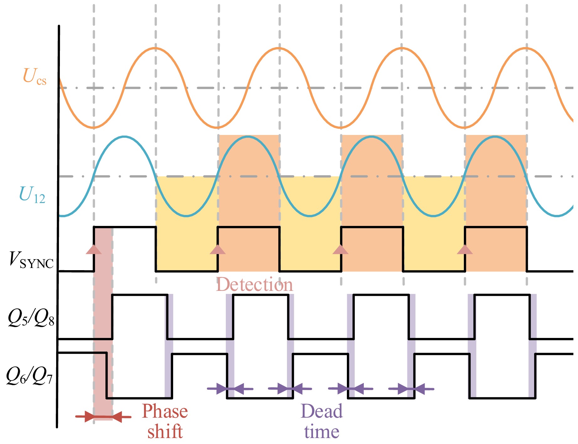
Figure 5.
Time sequence diagram of the proposed SR method signal.
ZVS analysis of the system
-
A topology that enables ZVS is required to achieve a highly efficient and high-power-density converter. The realization of zero-voltage switching (ZVS) requires careful consideration of the parasitic capacitances inherent in power devices such as MOSFETs and GaN transistors. To ensure ZVS operation, the circuit must satisfy the following conditions[25,26]:
$ \dfrac{1}{2}LI_1^2 \geqslant {Q_{oss}}({U_1}) \cdot {U_1} $ (18) There, QOSS(U1) denotes the charge stored in the MOSFET's parasitic output capacitance COSS when the drain voltage is U1. To mitigate the losses caused by hard switching in most MOSFETs, ZVS is commonly employed to achieve soft switching. This requires an additional inductor current, which charges and discharges the parasitic capacitance of the relevant MOSFET.
For GaN and Si devices, switching losses are primarily concentrated in turn-off losses. Therefore, it is crucial to ensure that the charge QOSS(U1) is fully discharged before switching transitions occur. Under these conditions, the voltage and current at the switching device should exhibit weak inductive characteristics. By sacrificing a small amount of non-resonant conduction loss, turn-off losses in the switching device can be significantly reduced.
For the inverter to achieve ZVS, the input impedance Zin must exhibit inductive characteristics. In this experimental design, weak inductance is achieved by fine-tuning the resonant capacitor, thereby increasing the inductive component of Zin at the original Zero Phase Angle (ZPA) point.
Due to the constant current source characteristics of the S–S compensation network, as described in Eqs (1) and (4), the resonant network and compensation capacitor remain unaffected by changes in the equivalent load Req. Instead, Req only alters the phase angle, as given in Eq. (6). Based on the turn-off current IOFF of both the converter and the MOSFET, as well as the stability of the ZVS condition, the value of IOFF for the reactance XS can be derived from Eqs (4) and (6) as follows:
$ {I_{OFF}} = - \dfrac{{2{U_1}{X_S}}}{{\pi {\omega ^2}{M^2}}} $ (19) From this equation, it can be deduced that there exists a maximum value of |XS|, denoted as XS,max, for the turn-off current IOFF, which enables the MOSFET to achieve complete ZVS. The following equation can be derived:
$ {X_{S,\max }} = - {\omega ^2}{M^2}\pi \sqrt {\dfrac{{{Q_{OSS}}({U_1})}}{{2{U_1}{L_p}}}} $ (20) Thus, the resonant parameters can be calculated based on the value of XS,max.
Since a full-bridge inverter is used in this experiment, U1 is half of the input voltage of a half-bridge inverter. Therefore, the design value of XS,max in this experiment, is expressed as:
$ {X_{S,\max }} = - {\omega ^2}{M^2}\pi \sqrt {\dfrac{{{Q_{OSS}}(0.5{U_1})}}{{2{U_1}{L_p}}}} \geqslant {X_S} $ (21) Phase angle constraint conditions for achieving ZVS in synchronous rectification and BWPT were proposed[27,28]. Here, θin and θout represent the input impedance angles as defined in Eqs (6) and (9), respectively. Here, φp denotes the phase difference between the primary-side voltage θU1 and current θI1, with Dp as the duty cycle of the primary switches. Likewise, φs represents the phase difference between the secondary-side voltage θU2 and current θI2, while Ds is the duty cycle of the secondary switches.
$ \left\{ {\begin{array}{*{20}{l}} {{\varphi _p} = {\theta _{uin}} - {\theta _{i1}}} \\ {{\varphi _s} = {\theta _{uout}} - {\theta _{i2}}} \end{array}} \right. $ (22) Neglecting parasitic parameters, φp can be approximated as θin, and φs as θout. According to the phase angle constraints for synchronous rectification presented in, the conditions for φp and φs are as follows[29]:
$ \left\{ {\begin{array}{*{20}{l}} {0 \leqslant {\varphi _p} \leqslant \dfrac{\pi }{2}{D_p}} \\ {0 \leqslant {\varphi _{\text{s}}} \leqslant \dfrac{\pi }{2}{D_s}} \end{array}} \right. $ (23) Using the values in Table 1, system parameters together with Eqs (1), (2), (19), and (20), the ZVS boundary conditions and network resonance are:
Table 1. System parameters.
Parameters Symbol Value Input voltage Uin 12−48 V Primary inductance Lp 1.79 μH Primary resonant capacitor Cp 15.5 nF Primary internal resistances Rp 23 mΩ Coil spacing d 10 mm Coupling coefficient k 0.32 Load resistance RL 5 Ω Secondary inductance Ls 1.77 μH Secondary resonant capacitor Cs 13.5 nF Secondary internal resistances Rs 28 mΩ Switching frequency fSW 1 MHz GaN's output capacitance Qoss 50 nC Although XS,max is very small, between 0 and 0.02 Ω, it is not zero; Fig. 6a shows how XS,max varies with frequency. Combining these constraints yields the ZVS operating range in Fig. 6b, where ZVS is achieved when:
$ {\text{0.9582}}\;{\text{MHz}} \lt {f_{{\text{ZVS}}}} \lt 1.0238\;{\text{MHz}} $ (24) Under the design conditions of Table 2, choosing fSW = fZVS places the system firmly within this ZVS region. Operating slightly off resonance to satisfy the ZVS criteria introduces a small amount of additional conduction loss but substantially reduces switching loss, leading to a significant improvement in overall system efficiency.
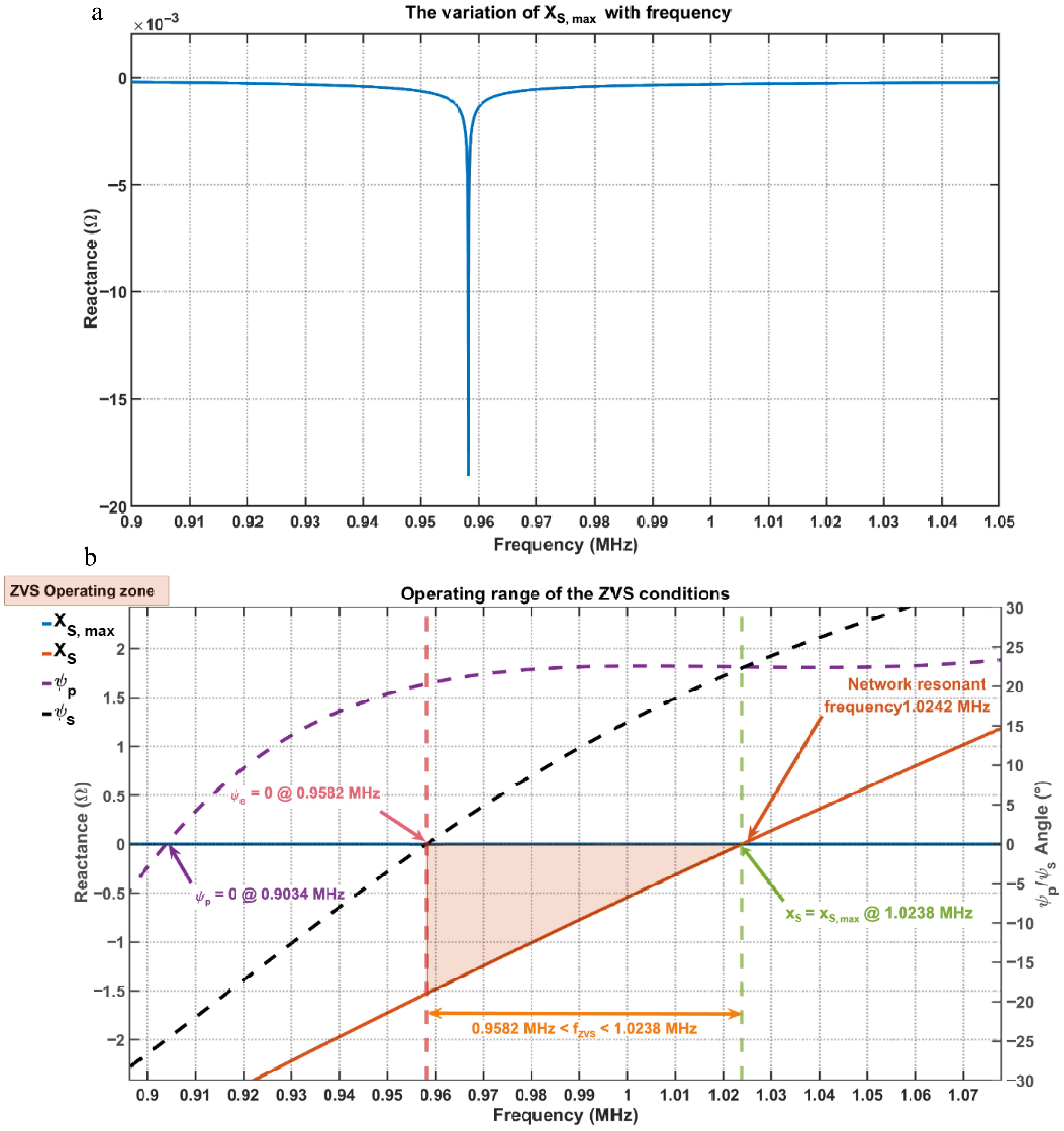
Figure 6.
Operating range of the ZVS conditions. (a) The variation of XS,max with frequency. (b) The range of ZVS.
Table 2. The ZVS boundary conditions and network resonance.
ZVS boundary conditions Switching frequency (fSW) (MHz) φp = 0 0.9034 φs = 0 0.9582 XS = XS,max 1.0238 Network resonance: XS = 0 1.0242 -
This experiment employs a hollow coil along with an integrated design of the compensation capacitor and converter. This integrated design benefits from allowing for precise signal acquisition while minimizing electromagnetic interference from the coil. In light of these considerations and the proposed method, an experimental platform was established, as shown in Fig. 7.
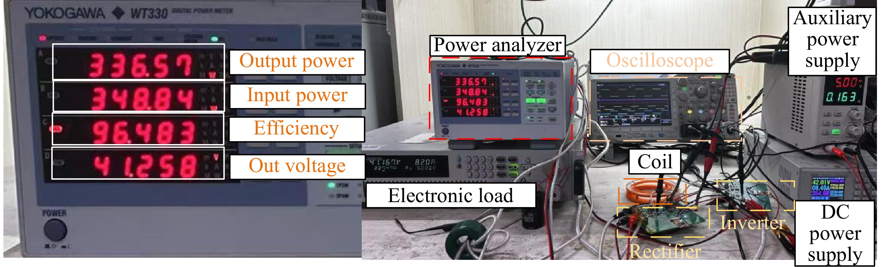
Figure 7.
Experimental platform and max efficiency.
In this experiment, the system operates at a switching frequency of 1 MHz, and the coupling coil has a diameter of 1 mm. The coils feature an air-core design and are constructed using multi-strand Litz wire along with 3D-printed components. The type of resonant capacitors is the NP0 capacitors. Both the primary and secondary converters are implemented on identical PCB boards with the same components, employing full-bridge converter topologies. The switching devices are GaN (ISG32001) components, with power diodes (NSR20F40NXT5G) paralleled with GaN devices to protect the system. The main control boards are built on the FPC (Flexible Printed Circuit) module. The control chip used on both sides is the C2000 MCU (TMS320 F2800137), and the high-speed comparator employed is GS8743. A 42V DC power supply provides the transmission power, while a 5.5 V auxiliary power supply powers the main control MCU, gate drive circuits, and comparators. The load is a 5 Ω constant-resistance electronic load, and a power analyzer is used to measure transmission efficiency. The specific experimental parameters are listed in Table 1, where Uout represents the output voltage, d represents the distance between the two coils, and k is the coupling coefficient of the coupled coil. According to the datasheet of the GaN device (ISG32001), the value of Qoss is obtained. Here, td represents the dead time, and D is the duty cycle of the switching square wave.
In WPT systems, the secondary side often employs passive rectification. This approach stems from the difficulty in synchronizing the oscillators and MCU clock frequencies between the primary and secondary sides, leading to challenges in aligning gate drive signal periods without auxiliary synchronization mechanisms. Traditional BIPT systems typically require communication lines, current transformers, or auxiliary coils to synchronize the MCU or gate signals on both sides. This paper proposes a method utilizing a high-speed comparator to perform the ZCD on the voltage across the secondary compensation capacitor. By implementing this technique, signal synchronization between the secondary and primary sides is achieved. The following section presents experimental verification of the ZCD method under the design parameters listed in Table 1, System parameters, demonstrating SR at a 1 MHz switching frequency.
Experimental results
-
Based on the mentioned theories and analyses, an experimental platform was established to validate the proposed method. The experimental waveform of the secondary-side synchronous signal is shown in Fig. 8a. At the switching frequency of 1 MHz, the voltage waveform across the compensation capacitor Cs, denoted as Ucs, is observed. Due to the high amplitude of Ucs, it cannot be directly connected to the high-speed comparator. Therefore, after passing through a common mode circuit, it eliminates harmonic signals, it avoids the influence of the rectifier switch tube, and makes the Ucs a sinusoidal voltage. Then, in its divider circuit, ZCD is performed using the comparator, resulting in the synchronous signal Ucs. This signal is then utilized by the MCU to synchronize the clock and gate drive signals on the secondary side, producing synchronized gate signals for Q5/Q8, as illustrated in Fig. 8c. In Fig. 8a, the ZCD signal Us and the Q5/Q8 pulse emitted by the secondary-side MCU achieve stable synchronization. By dead time and phase settings in the MCU, synchronization is also maintained for Q6/Q7, as shown in Fig. 8c. Ultimately, this method achieves signal synchronization between the secondary and primary sides without the use of current transformers, communication methods, or auxiliary coils.
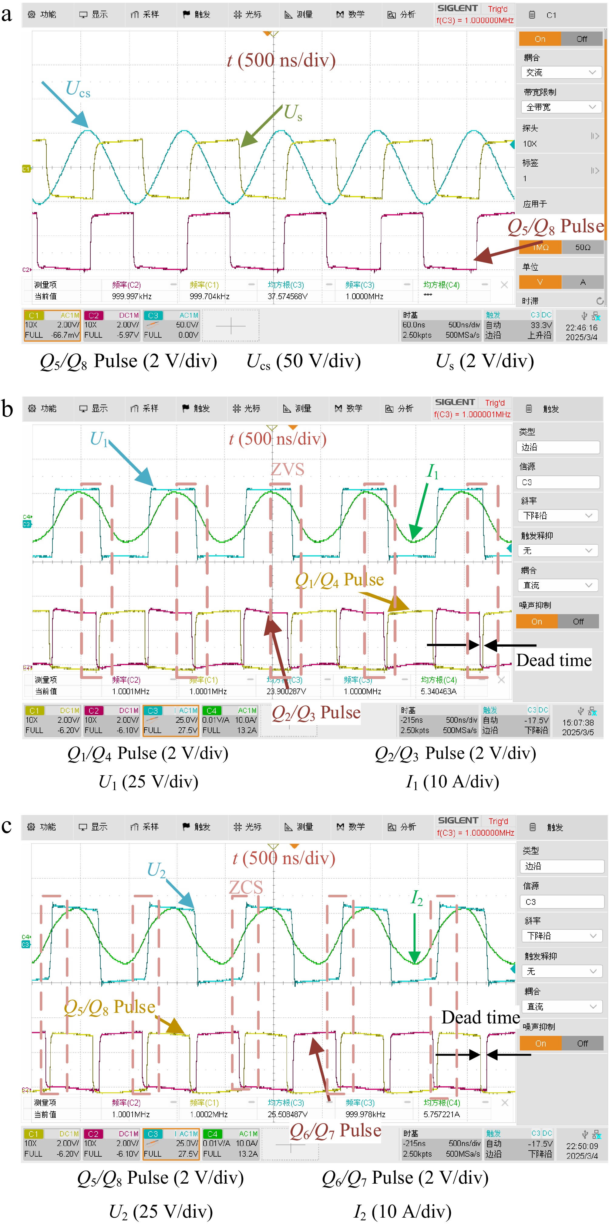
Figure 8.
Soft-switching and synchronous signal. (a) Secondary synchronous signal sampling experimental waveform. (b) Primary waveform. (c) Secondary waveform.
Under operating conditions of a constant input voltage Uin = 24 V, a constant-voltage electronic load output Uout = 24 V, and a system switching frequency of 1 MHz, ZVS is achieved through the MCU's dead-time control of the GaN drive signals and the compensation capacitors. Fig. 8b illustrates the primary side's waveform of ZVS and GaN's gate control signals. By maintaining the switching frequency of 1 MHz on the primary side and appropriately configuring the resonant network and dead time settings, ZVS is realized on the primary side. In Fig. 8b, U1 represents the inverter voltage, I1 denotes the current, and Q1/Q4 and Q2/Q3 correspond to the gate signals of the primary-side GaN switches.
Under operating conditions with a constant input voltage Uin = 24 V, a constant resistance electronic load RL = 5 Ω, and a system switching frequency of 1 MHz, ZVS was achieved through the MCU's dead-time control of the GaN drive signals and the use of compensation capacitors. As shown in Fig. 8b, the primary waveform illustrates the primary side's soft-switching waveform and the gate control signals of the GaN devices. By maintaining a 1 MHz switching frequency on the primary side and appropriately configuring the resonant network and dead-time settings, ZVS was successfully implemented. In Fig. 8b, U1 represents the inverter's output voltage, i1 denotes the inverter's output current, and Q1/Q4 and Q2/Q3 correspond to the gate signals of the primary side GaN switches.
Based on the theory presented in the SR method and as illustrated in Fig. 8a, stable synchronization signals were obtained during experiments. After implementing phase shifting and dead-time adjustments, the secondary MCU effectively synchronizes the operation of switches Q5, Q6, Q7, and Q8 with the primary switches Q1, Q2, Q3, and Q4. This synchronization eliminates potential frequency discrepancies and unstable phase differences between the primary and secondary switches, thereby preventing erroneous conduction that could lead to secondary-side short circuits.
Similarly, in Fig. 8c, U2 represents the voltage entering the rectifier from the compensation capacitor, i2 denotes the corresponding current, and Q5/Q8 and Q6/Q7 are the gate signals for the secondary GaN devices. Through the combined effects of the compensation network and appropriate dead-time settings, soft-switching was achieved on the secondary side. The low on-resistance of active devices reduced the voltage drop losses associated with passive rectifier power diodes, thereby enhancing system efficiency at a 1 MHz switching frequency. Under these operating conditions, the system achieved a maximum efficiency of ηmax = 96.48% and an output power of 336.57 W, as depicted in Fig. 7.
Under the constant resistance mode of the electronic load with RL = 5 Ω, the system was tested at input voltages Uin of 12, 18, 24, 30, 36, 42, and 48 V. As shown in Fig. 9, both output power Pout and efficiency η vary with the input voltage. Across all tested conditions, the overall system efficiency remained above 96%. The max efficiency η of 96.48% was achieved at an input voltage of 42 V, corresponding to Pout of 336.57 W. Throughout the tested voltage range of 12–48 V, the primary side consistently operated under ZVS, while the secondary side maintained soft switching and low-loss performance through synchronous rectification. This rectification scheme ensured high efficiency and strong system stability.
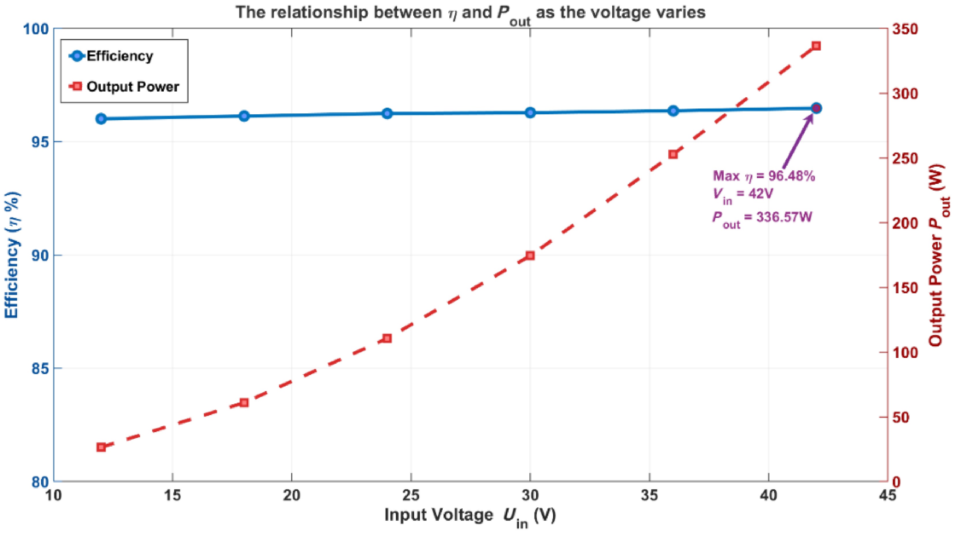
Figure 9.
Relationship between η and Pout when the Req is 5 Ω.
A comprehensive loss analysis of the system is presented here. It should be noted that the GaN gate drivers and the MCU are powered by an auxiliary power supply; therefore, the losses associated with the auxiliary power supply are not included in the following analysis. As illustrated in Fig. 7, the total measured power loss in the system is 12.580 W. The power losses are categorized into four main components: inductor losses, capacitor losses, converter losses[30,31], and other losses[31,32]. The 'other losses' primarily include the effects of parasitic parameters on the PCB, losses in the power analyzer connection cables, and energy dissipation in the output bus capacitors across Uout. Based on a detailed analysis of the inductor, capacitor, and GaN device losses, the power distribution is summarized in Fig. 10. From this figure, it can be observed that inductor losses constitute the largest proportion of the total losses, followed by capacitor losses. The power loss contributed by GaN devices in the converter is only 2.533 W, accounting for 20.1% of the total. These results indicate that the proposed scheme demonstrates excellent efficiency on the converter side, achieving very low switching and conduction losses in the synchronous rectification stage.
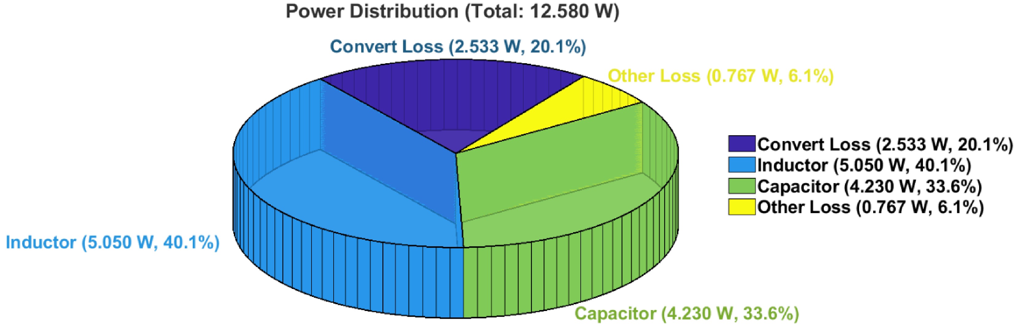
Figure 10.
Power loss distribution.
Comparison with other works
-
Compared to other SR methods listed in Table 3, the system proposed in this work demonstrates superior robustness in terms of efficiency. When compared with the same SS compensation network[34], the proposed method achieves higher efficiency even at a higher switching frequency. Additionally, in comparison with the Class-E converters[27], the proposed system still maintains a higher efficiency. Unlike Class-E converters, the full-bridge converter used in this experiment includes more switching devices. Despite the increased number of switches, the system still achieves efficient and highly stable power transfer. Across various SR strategies and compensation networks, this solution consistently delivers high efficiency and stability. Moreover, the hardware implementation of the ZCD is cost-effective, offers reliable signal performance, and is less susceptible to electromagnetic interference. In comparison with highly integrated commercial SR chips, the proposed SR scheme exhibits superior performance under high-frequency operating conditions, with significantly reduced power loss. Moreover, it enables output power regulation through MCU-based control, offering greater flexibility and adaptability in system-level design and application. This makes the proposed approach not only more efficient but also more extensible and scalable for practical engineering implementations.
Table 3. Comparison with other works.
-
This paper proposed a synchronous rectification method with a high-speed comparator for a Megahertz frequency BWPT system. Although the experimental analysis in this study focuses solely on the SS topology, the proposed synchronous rectification scheme is also applicable to other compensation topologies, such as dual-sided LCC, LLC-S, and dual-sided LLC. In these configurations, the scheme can similarly obtain complete synchronization signals, and achieve stable zero-crossing detection. Compared to integrated synchronous rectification (SR) chips, the proposed scheme offers superior frequency performance and significantly lower power losses. Furthermore, it provides a flexible platform for functional expansion and system-level customization. Unlike traditional approaches that rely on current transformers or auxiliary coils, this method directly connects the voltage across the secondary compensation capacitor to a comparator to acquire the synchronization signal. This signal is then processed by the MCU to achieve efficient SR on the secondary side. This method not only ensures high-precision synchronization between the primary and secondary sides but also simplifies system design and enhances overall integration. Therefore, this method reduces losses on the secondary side and enhances overall system efficiency, demonstrating high stability at a switching frequency of 1 MHz while delivering an output power of 336.57 W with a transmission efficiency of 96.48%. Additionally, the approach is minimally affected by electromagnetic interference, features a simple hardware implementation, and offers low cost, making it highly versatile and widely applicable.
This work was supported in part by the National Natural Science Foundation of China (Grant No. 52467023), in part by the Yunnan Fundamental Research Project (Grant No. 202401BE070001-061 and 202501CF070119), and in part by the Major Science and Technology Projects in Yunnan Province (Grant No. 202402AF080001).
-
The authors confirm contributions to the paper as follows: study conception and design: Liu Z, Sun Z, Rong E; data collection: Yang Y, Zou X, Shafiq Z; analysis and interpretation of results: Li S, Li T, Yang Y, Lu S; draft manuscript preparation: Yang Y, Liu Z; conceptualization, funding acquisition, and supervision: Li S, Liu Z. All authors reviewed the results and approved the final version of the manuscript.
-
The datasets generated and/or analyzed during the current study are available from the corresponding author upon reasonable request.
-
The authors declare that they have no conflict of interest.
- Copyright: © 2025 by the author(s). Published by Maximum Academic Press, Fayetteville, GA. This article is an open access article distributed under Creative Commons Attribution License (CC BY 4.0), visit https://creativecommons.org/licenses/by/4.0/.
-
About this article
Cite this article
Li S, Yang Y, Rong E, Li T, Sun Z, et al. 2025. A synchronous rectification method with a high-speed comparator for a megahertz frequency BWPT system to enhance efficiency. Wireless Power Transfer 12: e031 doi: 10.48130/wpt-0025-0029 

A synchronous rectification method with a high-speed comparator for a megahertz frequency BWPT system to enhance efficiency
- Received: 29 April 2025
- Revised: 07 July 2025
- Accepted: 25 August 2025
- Published online: 28 November 2025
Abstract: In bidirectional wireless power transfer (BWPT) systems, the phase synchronization accuracy of the secondary synchronous rectification (SR), or active rectification signal directly determines energy transfer efficiency and overall system stability. In traditional SR solutions, current transformers increase system losses. The auxiliary coil and RF line connection are susceptible to electromagnetic interference, resulting in signal delays, that lead to reduced system efficiency. This paper proposes a secondary-side self-synchronized rectification method that utilizes a high-speed comparator to perform real-time zero-crossing detection (ZCD) of the voltage across the secondary compensation capacitor, thereby generating a synchronization signal on the secondary side. By sampling the compensation capacitor, the obtained synchronization signal demonstrates high stability and strong immunity to interference. By studying synchronization signal acquisition at a switching frequency of 1 MHz, the proposed method enhances the stability of secondary-side synchronous rectification, enables soft switching, reduces system losses, and supports high-efficiency BWPT at 1 MHz. In this experiment, a BWPT system prototype incorporating a synchronous rectification method was developed. The system utilizes GaN devices in combination with an S-S compensation network and operates at a frequency of 1 MHz. SR is achieved on the secondary side, delivering an output power of 336.57 W, with a transmission efficiency of 96.48%.