


-
Electrically excited synchronous machines (EESMs) are attractive for traction because they avoid rare-earth magnets and allow tunable field strength[1,2]. As brushes and slip rings are replaced by inductive wireless power transfer (WPT) to feed the rotor[3,4], excitation becomes contactless and the central control task shifts to robustly inferring the rotor field current from primary-side measurements[5,6]; this feasibility depends strongly on the chosen resonant topology and on the typically strong coupling imposed by compact layouts.
Recent studies have begun to treat rotor-field inference itself as a primary estimation problem in contactless excitation. For inductively excited EESMs, model-based approaches estimate rotor field current (and sometimes temperature) from transmitter-side variables, and show experimental validation[7−9]; related brushless-exciter work likewise closes the loop without rotor sensors. In parallel, primary-side-only identification/regulation has been demonstrated for common WPT links[10,11], using inverter voltage/current—sometimes with phase—to infer load/output and thus avoid receiver instrumentation or communication. These trends support a topology–measurement co-design centered on what is reliably available at the transmitter.
Across the WPT design space, high coupling coefficients (k) can degrade the fidelity of the first-harmonic approximation (FHA)[12], leading to frequency splitting, waveform distortion, and heightened parameter/phase sensitivity—especially under detuning or light-load conditions—so time-domain/differential-equation models are often required[13]. The typical waveform distortion and discontinuous current phenomena caused by such strong coupling are illustrated in Fig. 1. In practice, S-S compensation is used for EESM wireless excitation[14], and LCL-S are also used to reduce receiver hardware[15]; however, under strong coupling or detuning, prior studies report distortion and sensitivity that complicate phase-based regulation and stress prediction, again motivating beyond-FHA modeling.
To minimize rotating hardware, the None-side (N) family removes secondary compensation—most notably S-N[16], LCL-N[17], LCC-N[18], LC-N[19], and even N-N[20]. Under high k and certain operating regions, shaped input impedances and diode thresholds can introduce rectifier input current conduction gaps (DCM) on the receiver[21,22], weakening CC/CV characteristics or soft-switching margins; accurate analysis in such regions typically relies on time-domain formulations rather than FHA. In LCC-N, CC/CV can be regulated using only transmitter-side voltage and current[23]; however, inferring the output from the resonant-capacitor voltage together with the primary current typically requires precise, high-bandwidth amplitude/phase sensing at the resonant frequency. For N-N and other sensor-minimal links, transmitter-only metering/estimation of delivered power and load is feasible, but errors grow at low output current, so schemes centered on robust transmitter observables are preferred. The S-N resonant topology maintains low harmonic distortion and avoids receiver-side current discontinuity under strong coupling conditions, making it particularly suitable for wireless excitation systems. However, its constant-voltage output characteristic causes the excitation current to vary with load changes, necessitating estimation algorithms to determine actual current values.
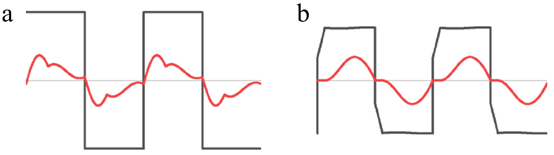
Figure 1.
Effects of strong coupling on system performance. (a) High harmonic content. (b) Discontinuous current mode.
Positioned in this context, this paper focuses on strongly coupled S-N. It derives a time-domain relationship between the excitation current and primary variables Udc, I1_rms, θ, and compares five primary-side estimation schemes under realistic detuning and sampling conditions. Experimental results indicate that the calculated method for obtaining cosθ achieves the best trade-off, maintaining low error while avoiding high-precision secondary-side phase sensing. This study provides a closed-loop control solution for wireless excitation systems under the S-N topology.
-
The exploded assembly diagram of the S-N topology wireless excitation system is shown in Fig. 2. It primarily consists of a high-frequency inverter, resonant capacitor, rotary magnetic coupler, the secondary side Printed Circuit Board (PCB), and an electrically excited motor. The absence of a resonant topology on the receiver side reduces rotational mechanical stress. The rotary magnetic coupler is divided into a primary side and a secondary side. The secondary side PCB feeds current into the excitation windings. During motor operation, the secondary side of the rotary magnetic coupler, the secondary side PCB, and the motor rotor rotate coaxially to remain relatively stationary.
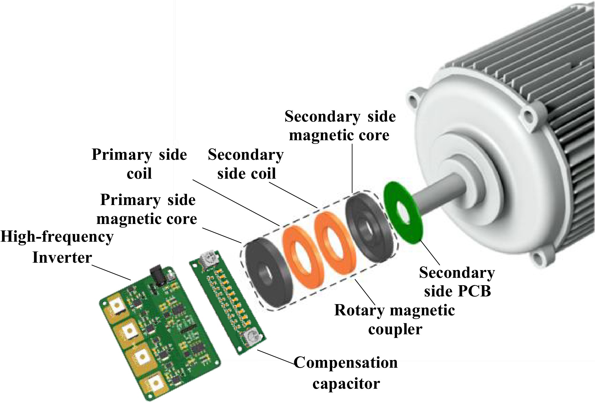
Figure 2.
Exploded diagram of S-N topology wireless excitation system.
The system circuit diagram of the S-N resonant topology is shown in Fig. 3. In the figure, Uin represents the input voltage, Qbuck, Dbuck, and Lbuck respectively represent the MOSFET, diode, and filter inductor that constitute the buck circuit. Udc represents the output voltage of the buck circuit, Cf1 is the filter capacitor, MOSFETs Q1–Q4 form the high-frequency inverter, and CP is the primary side resonant capacitor. The parts enclosed by the red boxes represent the rotary magnetic coupler. The model in Fig. 3a is the mutual inductance model, the model in Fig. 3b is the single leakage inductance model for the primary side, used to reveal the circuit operation mechanism of the S-N resonant topology. Diodes D1–D4 form the rectifier circuit, Cf2 is the receiver-side filter capacitor, and Lf and Rf denote the equivalent excitation inductance and resistance, respectively.
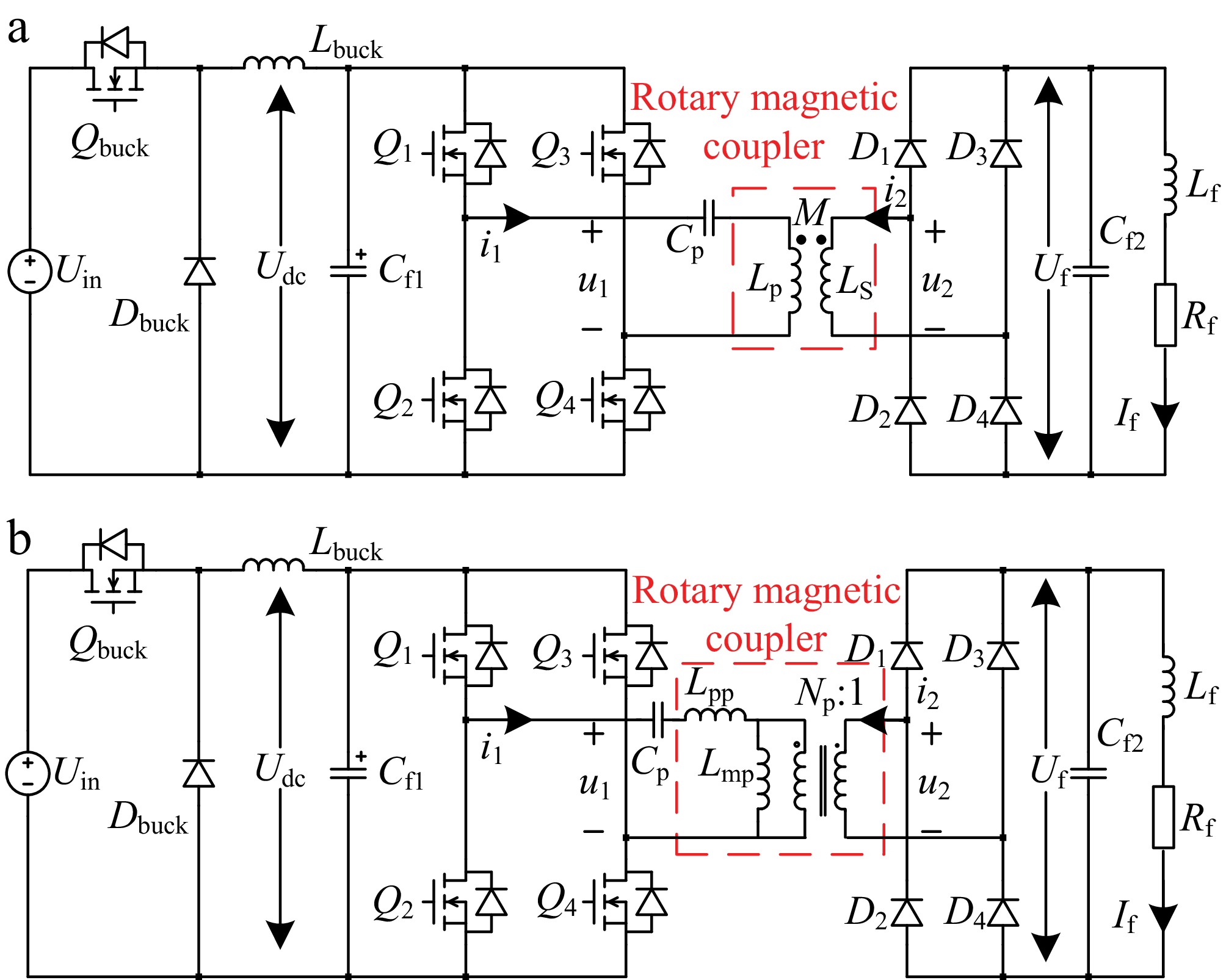
Figure 3.
Wireless excitation systems with S-N topology based on different equivalent models. (a) Based on mutual inductance model. (b) Based on single leakage inductance model.
In the figure, u1 and u2 represent the output voltage of the high-frequency inverter and the input voltage of the rectifier, respectively, i1 and i2 represent the currents flowing through the primary and secondary sides of the rotary magnetic coupler, respectively, and Uf and If represent the voltage across the excitation winding and the excitation current, respectively.
In the mutual inductance model, the magnetic coupler consists of the self-inductance LP of the primary side, the self-inductance LS of the secondary side, and the mutual inductance M. In the single leakage inductance model, it consists of the leakage inductance Lpp of the primary side, the magnetizing inductance Lmp, and an ideal transformer with a turn ratio of Np:1.
The expressions for the parameters of the single leakage inductance model can be derived as follows:
$ \left\{ \begin{gathered} {N_{\text{P}}} = \dfrac{M}{{{L_{\text{S}}}}} \\ {L_{{\text{mp}}}} = \dfrac{{{M^2}}}{{{L_{\text{S}}}}} \\ {L_{{\text{pp}}}} = {L_{\text{P}}} - \dfrac{{{M^2}}}{{{L_{\text{S}}}}} = \left( {1 - {k^2}} \right){L_{\text{P}}} \\ \end{gathered} \right. $ (1) In the equation, k is the coupling coefficient, and it satisfies:
$ k = \dfrac{1}{{\sqrt {{L_{\text{P}}}{L_{\text{S}}}} }} $ (2) In the S-N resonant topology, the resonant capacitance value should satisfy:
$ {C_{\text{P}}} = \dfrac{1}{{{\omega ^2}{L_{{\text{pp}}}}}} $ (3) where, ω represents the operating frequency of the system. Under these conditions, the system voltage satisfies:
$ \dfrac{{{u_1}}}{{{u_2}}} = \dfrac{{{U_{{\text{dc}}}}}}{{{U_{\text{f}}}}} = \dfrac{{{N_{\text{P}}}}}{1} $ (4) -
In pursuit of high power density and miniaturization, wireless excitation systems are often subject to strict spatial constraints, leading to strong magnetic coupling[24]. Under such conditions, higher-order harmonics become pronounced, limiting the accuracy of simplified harmonic models. To maintain modeling fidelity, the system is characterized using a time-domain, differential-equation formulation.
Equation (5) is the system KVL equation, Eqs. (6) and (7) represent the expressions for voltages u1 and u2, respectively, and Eq. (8) is the initial condition.
$ \left\{ \begin{gathered} {u_1} = {u_{{\text{Cp}}}} + {L_{\text{P}}}\dfrac{{d{i_1}}}{{dt}} + M\dfrac{{d{i_2}}}{{dt}} + {R_1}{i_1} \\ {u_2} = {L_{\text{S}}}\dfrac{{d{i_2}}}{{dt}} + M\dfrac{{d{i_1}}}{{dt}} + {R_2}{i_2} \\ {i_1} = {C_{\text{P}}}\dfrac{{d{u_{{\text{Cp}}}}}}{{dt}} \\ {u_1} - {R_1}{i_1} - {u_{{\text{Cp}}}} - (1 - {k^2}){L_{\text{P}}}\dfrac{{d{i_1}}}{{dt}} = {N_{\text{P}}}\left( {{u_2} - {R_2}{i_2}} \right) \\ \end{gathered} \right. $ (5) $ {u_1} = \left\{ \begin{array}{*{20}{l}} {{U_{{\text{dc}}}}}&{0 \leqslant t \lt \dfrac{{\text{π }}}{\omega }} \\ { - {U_{{\text{dc}}}}}&{\dfrac{{\text{π }}}{\omega } \leqslant t \lt \dfrac{{{\text{2π }}}}{\omega }} \end{array} \right. $ (6) $ {u_2} = \left\{ \begin{gathered} \begin{array}{*{20}{c}} {{U_{\text{f}}} + 2{U_{\text{d}}}}&{0 \leqslant t \lt \dfrac{{\text{π }}}{\omega }} \end{array} \\ \begin{array}{*{20}{c}} { - \left( {{U_{\text{f}}} + 2{U_{\text{d}}}} \right)}&{\dfrac{{\text{π }}}{\omega } \leqslant t \lt \dfrac{{{\text{2π}}}}{\omega }} \end{array} \\ \end{gathered} \right. $ (7) $ \left\{ \begin{gathered} {i_1}(0) = - {i_1}\left( {\frac{{\text{π }}}{\omega }} \right) = {i_1}\left( {\frac{{{\text{2π}}}}{\omega }} \right) \\ {i_2}(0) = - {i_2}\left( {\frac{{\text{π }}}{\omega }} \right) = {i_1}\left( {\frac{{{\text{2π }}}}{\omega }} \right) \\ {u_{{C_{\text{P}}}}}(0) = - {u_{{C_{\text{P}}}}}\left( {\frac{{\text{π }}}{\omega }} \right) = {u_{{C_{\text{P}}}}}\left( {\frac{{{\text{2π }}}}{\omega }} \right) \\ {i_2}(0) = 0 \\ \end{gathered} \right. $ (8) where, R1 and R2 denote the parasitic resistances on the primary and secondary sides, respectively, and Ud denotes the diode forward-voltage drop. By solving the differential equations, it is obtained that the primary side current i1 maintains a sinusoidal waveform throughout the entire cycle. The secondary side current i2 comprises two components: a sinusoidal waveform i2_sin, and a triangular waveform i2_tri. The sinusoidal component exhibits 180° phase reversal relative to i1. The expressions for currents i1 and i2 are derived as:
$ {i_1} = \dfrac{{{\text{π }}U_{\rm{dc}}^{'}{L_{\rm S}}}}{{2\omega {M^2}\sin \theta }}\sin (\omega t - \theta ) $ (9) $ {i_2} = \left\{ \begin{gathered} - \dfrac{{{\text{π }}U_{\rm{dc}}^{'}}}{{2\omega M\sin \theta }}\sin (\omega t - \theta ) + \dfrac{{U_{\rm{dc}}^{'}}}{M}t - \dfrac{{{\text{π }}U_{\rm{dc}}^{'}}}{{2\omega M}},0 \leqslant t \lt \dfrac{{\text{π }}}{\omega } \\ - \dfrac{{{\text{π }}U_{\rm{dc}}^{'}}}{{2\omega M\sin \theta }}\sin (\omega t - \theta ) - \dfrac{{U_{\rm{dc}}^{'}}}{M}t + \dfrac{{{\text{3π}}U_{\rm{dc}}^{'}}}{{2\omega M}},\frac{{\text{π }}}{\omega } \leqslant t \lt \dfrac{{2{\text{π }}}}{\omega } \\ \end{gathered} \right. $ (10) where, U'dc is given by:
$ U_{\rm{dc}}^{'} = {U_{\rm{dc}}} - \frac{{2\sqrt 2 {I_{1\_{\rm{rms}}}}({R_1} + {R_2}{N_P}^2)\cos \theta }}{{\text{π }}} $ (11) Figure 4 illustrates the waveforms of voltages u1 and u2, current i1, and the constituent components of current i2, derived from their respective mathematical expressions. The waveform analysis demonstrates that:
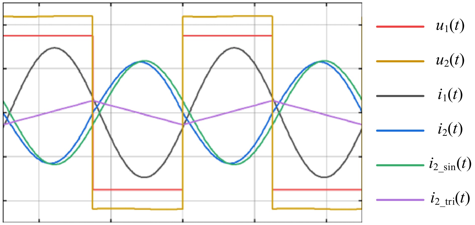
Figure 4.
Voltage and current waveforms of primary and secondary sides.
The triangular component of the secondary current i2_tri is 90° out of phase with the secondary voltage u2 and therefore delivers no active power to the load. A nonzero power angle θ between u1 and i1 arises because the resonant capacitor only partially compensates the leakage inductance, leaving residual reactive power in the link. This net inductive bias facilitates soft switching (ZVS) on the primary side.
Based on Eq. (10), and the principle of energy conservation[21], neglecting the diode voltage drop, the expression for the excitation current can be derived as:
$ {I}_{\text{f}}=\dfrac{2\sqrt{2}}{\text{π}}{i}_{{2\_{\rm{sinrms}}}}\mathrm{cos}\theta =\dfrac{{U}_{{\rm{dc}}}^{'}}{\omega M\mathrm{tan}\theta } $ (12) Meanwhile, the excitation current can also be expressed by the value of I1_rms.
$ {I_{\text{f}}} = \dfrac{{2\sqrt 2 }}{{\text{π }}}\dfrac{M}{{{L_{\rm S}}}}{i_{{\text{1\_rms}}}}\cos \theta $ (13) From the above equation, it can be seen that the excitation current can be estimated using the input voltage Udc and the power angle θ, and it can also be estimated using the RMS value of the primary current I1_rms and the power angle θ.
Principle of the excitation current estimation algorithm
-
The input voltage and primary current can be directly obtained through sampling, while there are two methods available to obtain the power angle θ.
The first method is the sampling method, which determines the power angle θ between u1 and i1 through Fourier decomposition of the sampled signals. To ensure the accuracy of θ, a high sampling rate is required, which imposes higher demands on device performance and increases system costs.
The second method is the calculation method, which utilizes the expression for the primary current i1 that contains sinθ. The angle θ can be obtained by sampling the RMS value of the transmitter-side current I1_rms. The calculation formula for θ is:
$ \theta = \arcsin \dfrac{{U_{_{{\text{dc}}}}^{'}{L_{\rm S}}}}{{4\sqrt 2 f{M^2}{I_{{\text{1\_rms}}}}}} $ (14) In the formula, f represents the system operating frequency, with the unit of Hertz (Hz). Based on the two excitation current estimation equations and the methods to obtain the power angle θ, five different excitation current estimation approaches can be derived, with their detailed descriptions summarized in the Table 1.
Table 1. Description of five estimation approaches.
Approach Methods to obtain θ Equation Sampling targets Approach 1 Calculation method Eq. (13) Udc I1_rms Approach 2 Calculation method Eq. (12) Udc I1_rms Approach 3 Calculation method Eq. (13) |u1| I1_rms Approach 4 Sampling method Eq. (12) Udc u1 i1 Approach 5 Sampling method Eq. (13) I1_rms u1 i1 Among the approaches, approach 3 calculates the power angle θ by replacing the input voltage Udc with the average value of the absolute values of the sampled voltage u1.
The estimated value derived from the estimation algorithm functions as the actual excitation current. Through comparison with the target value, the actual excitation current is regulated to track the target value, thus realizing closed-loop control of the system. According to the different estimation approaches, the overall control block diagram and the corresponding principal block diagrams can be drawn as shown in the Fig. 5. The diagrams mainly include three parts: the green part represents the calculation of the power angle θ, the blue part represents the calculation of intermediate quantities, and the orange part represents the calculation of the current If.
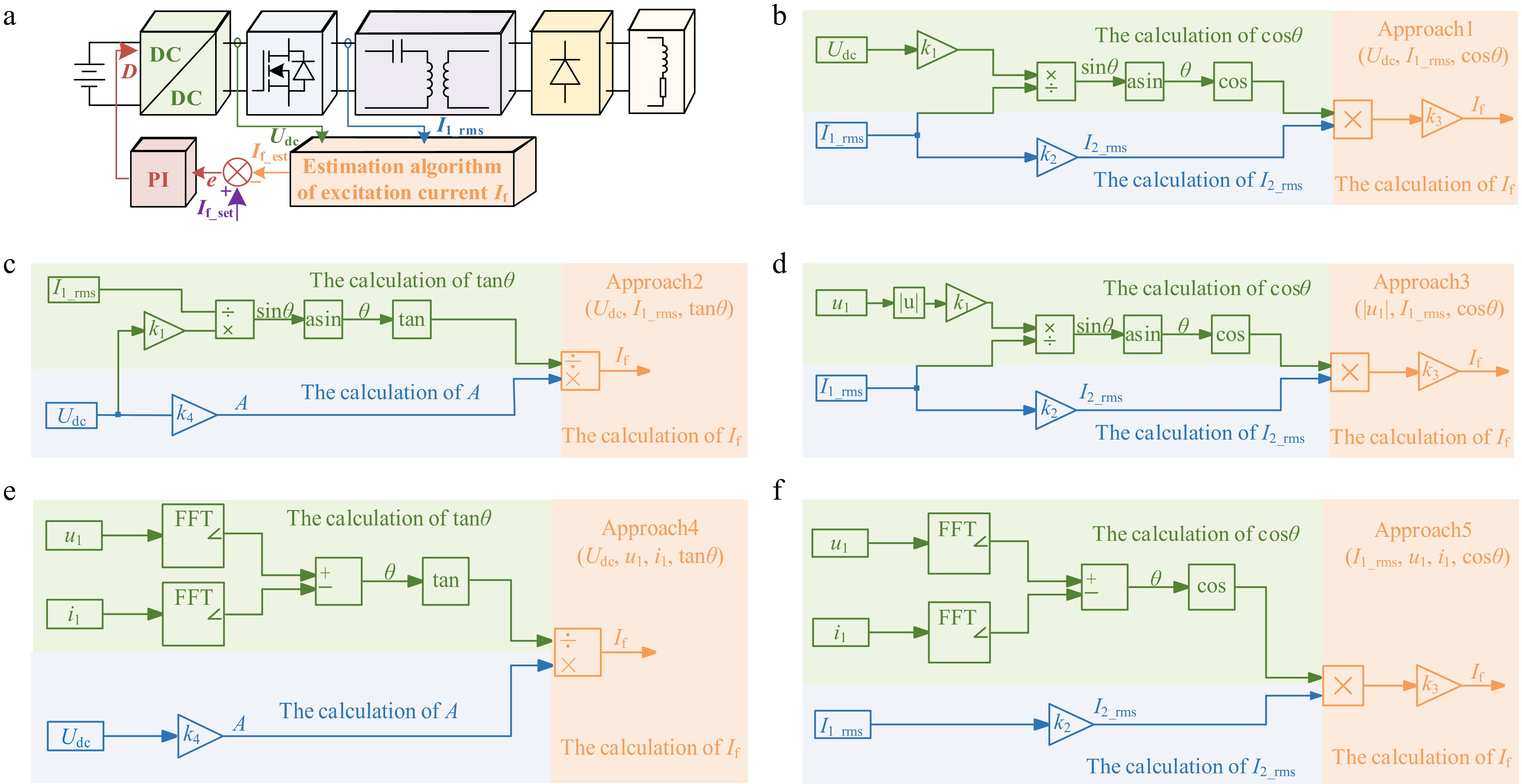
Figure 5.
Control block diagram of wireless excitation system and the principle block diagram of five different estimation approaches. (a) Control block diagram of wireless excitation system. (b) Principle block diagram of approach 1. (c) Principle block diagram of approach 2. (d) Principle block diagram of approach 3. (e) Principle block diagram of approach 4. (f) Principle block diagram of approach 5.
The values of k1, k2, k3, and k4 satisfy:
$ \left\{ {\begin{array}{*{20}{l}} {{k_1} = \dfrac{{{L_{\rm S}}}}{{4\sqrt 2 f{M^2}}}}&{{k_2} = \dfrac{M}{{{L_{\rm S}}}}} \\ {{k_3} = \dfrac{{2\sqrt 2 }}{{\text{π }}}}&{{k_4} = \dfrac{1}{{\omega M}}} \end{array}} \right. $ (15) Simulation comparison of five excitation current estimation approaches
-
To compare the performance of five different estimation approaches, a circuit simulation model is built in PLECS for verification. The specific parameter configurations are shown in Table 2.
Table 2. Parameters of S-N wireless excitation system.
Components Parameters Components Parameters Udc 24 V M 32.266 μH f 80 kHz CP 438.74 nF LP 33.756 μH Rf 4.3 Ω LS 42.09 μH Lf 180 mH Figure 6 shows the results of the phase angle θ obtained by the sampling method and calculation method under different sampling frequencies, where the sampling frequency of I1_rms in the calculation method is equal to that of the sampling method. In the figure, the black curve denotes the actual value of θ, the blue curve represents the sampled value, and the red curve indicates the calculated value. Notably, as the sampling frequency varies, the sampled value exhibits significant fluctuations, whereas the calculated value shows negligible variation and shows better agreement with the actual value.
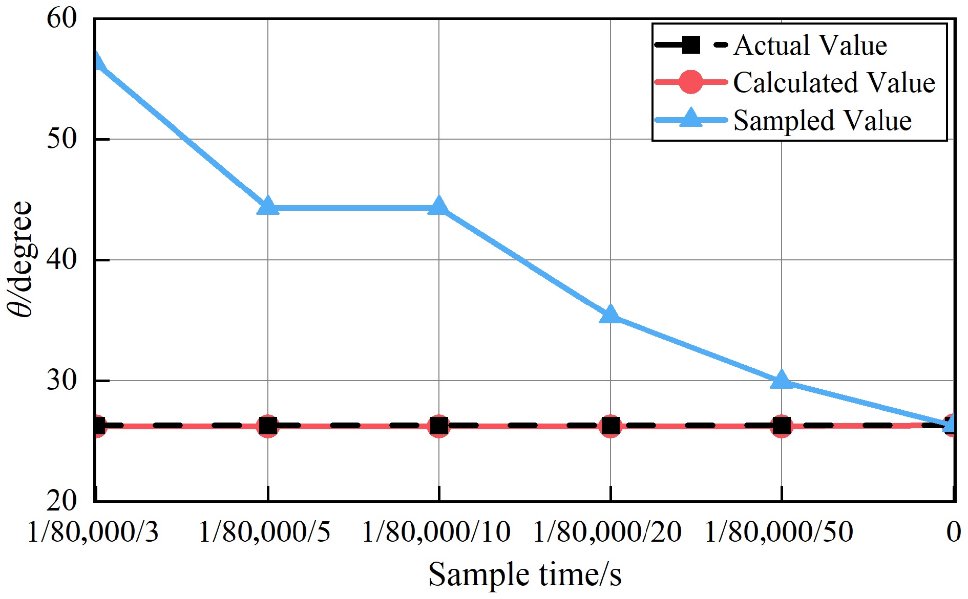
Figure 6.
The value of power angle θ obtained by different methods.
Interestingly, when the sampling frequencies are set to 400 and 800 kHz, the sampling method yields identical phase angle estimates. The time domain waveforms under the two sampling frequencies are depicted in Fig. 7. Notably, these waveforms exhibit obviously different characteristics under the respective sampling conditions, yet their FFT analysis results unveil a critical consistency: despite the obvious difference in amplitude, the phase differences under the two sampling frequencies remain perfectly consistent.
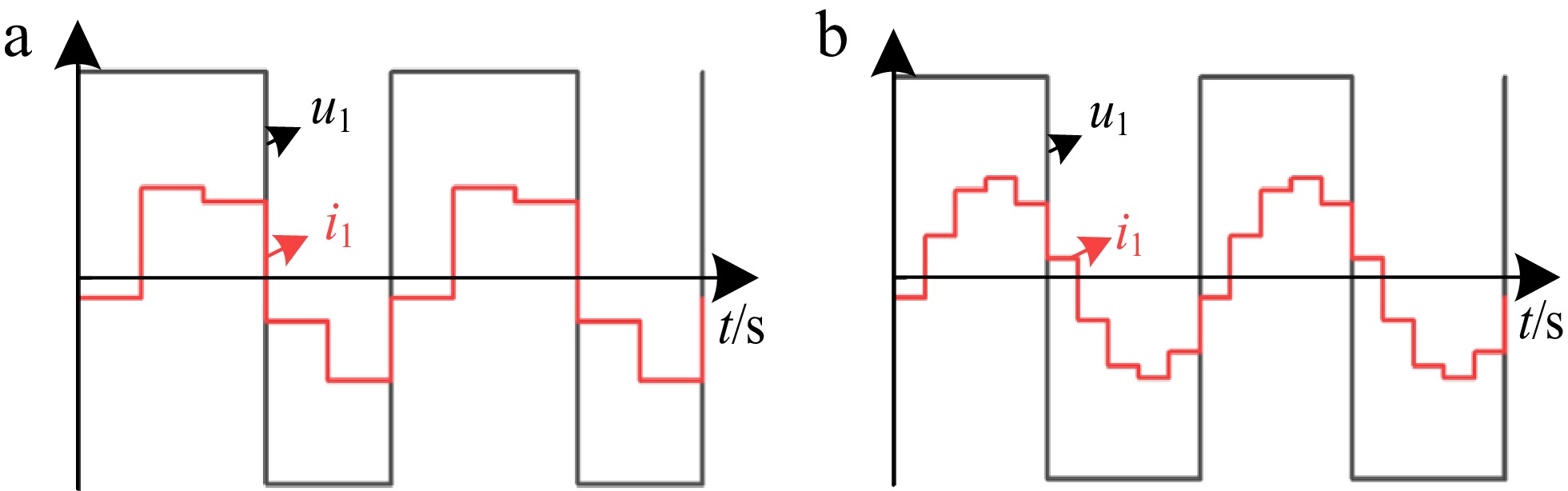
Figure 7.
Sampling waveforms of u1 and i1 at different sampling frequencies. (a) 400 kHz (five times f). (b) 800 kHz (ten times f).
With the sampling frequency fixed at 800 kHz, Fig. 8 compares the actual, calculated, and sampled values of the cosθ and tanθ of the θ. The significant error in the sampling method of θ leads to substantial deviations in both trigonometric functions. Meanwhile, the error of cosθ is far smaller than that of tanθ; thus, using cosθ for calculation is more reliable. The comparison between the estimated results of the five approaches and the actual values is shown in Fig. 9. The six color curves in the figure represent the estimated values of the five estimation approaches and the actual value of the excitation current respectively. It can be seen that approaches 1, 2, and 3 exhibit smaller errors relative to the actual value, and completely overlap with the actual value, while approaches 4 and 5 show larger discrepancies, primarily due to significant errors in the power angle θ obtained by the sampling method. A load change occurs at 0.59 s, with the excitation resistance Rf shifting from 4.3 to 6.4 Ω. After the sudden load variation, both the actual excitation current and the estimated values from the five approaches change accordingly. Notably, the estimated values from approaches 1, 2, and 3 remain close to the actual value, which demonstrates the load independence of the estimation approach.
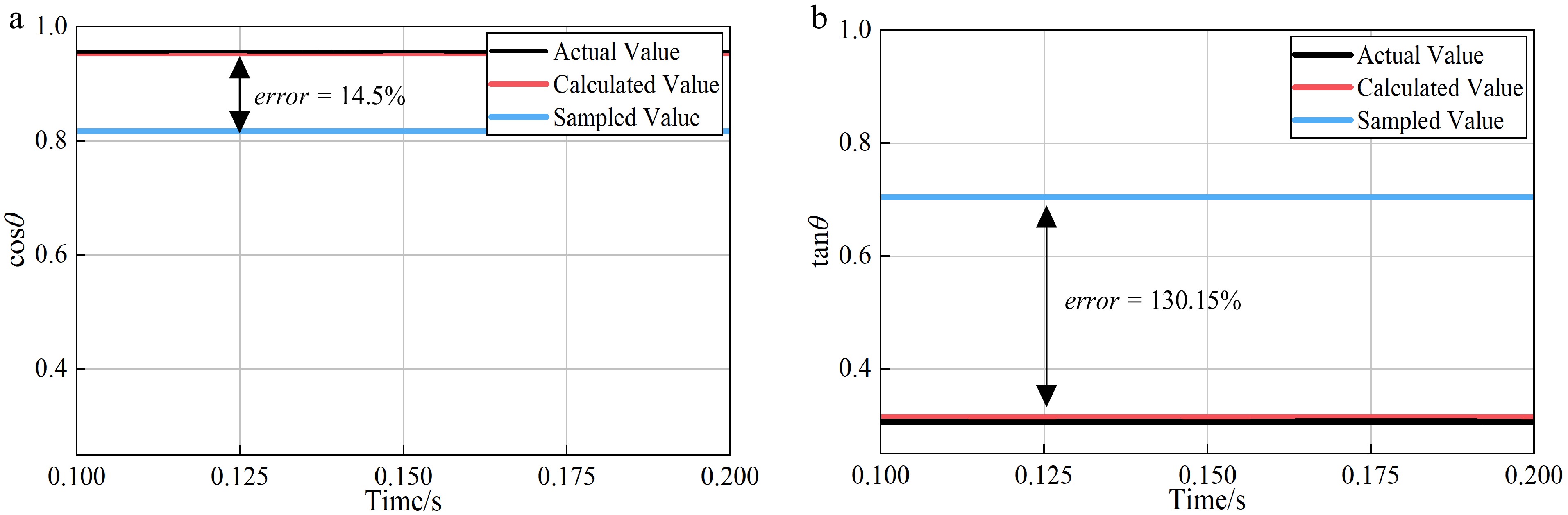
Figure 8.
The value of cosθ and tanθ obtained by different method. (a) The value of cosθ obtained by different methods. (b) The value of tanθ obtained by different methods.
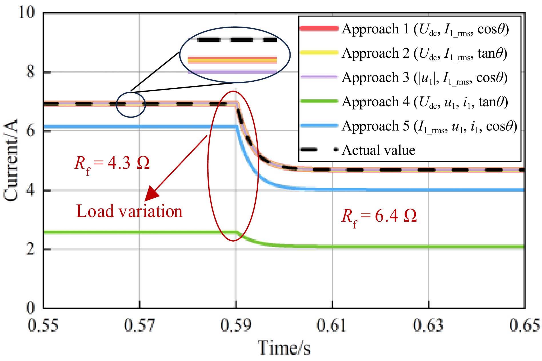
Figure 9.
Estimation results of five different estimation approaches.
A performance comparison of five different estimation approaches in various aspects is shown in Fig. 10. After comprehensive evaluation, Approach 1 is chosen as the final estimation algorithm scheme. It boasts the following advantages: only requiring sampling of Udc and I1_rms, featuring simple hardware implementation, imposing a moderate computational burden, being well-suited for real-time control, and maintaining stability during abrupt load fluctuations.
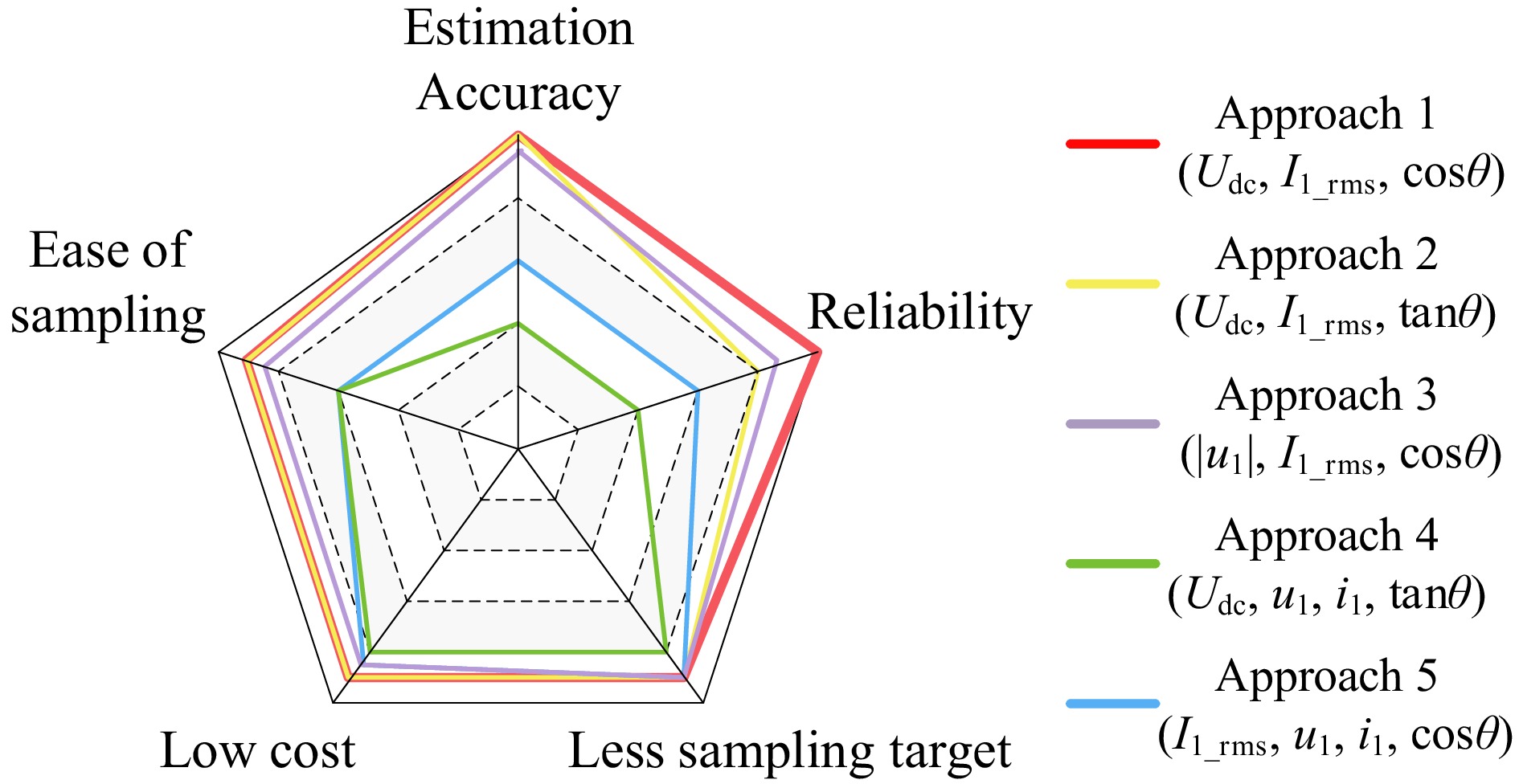
Figure 10.
Comparison radar chart of five different estimation approaches.
Notably, the expression for U'dc also contains cosθ. This motivates an iterative design: use the previous-step value cosθ(n−1) to compute U'dc, then update cosθ(n) accordingly. Once the system converges, cosθ(n) = cosθ(n−1), yielding the final estimate. The corresponding flowchart is shown in Fig. 11.
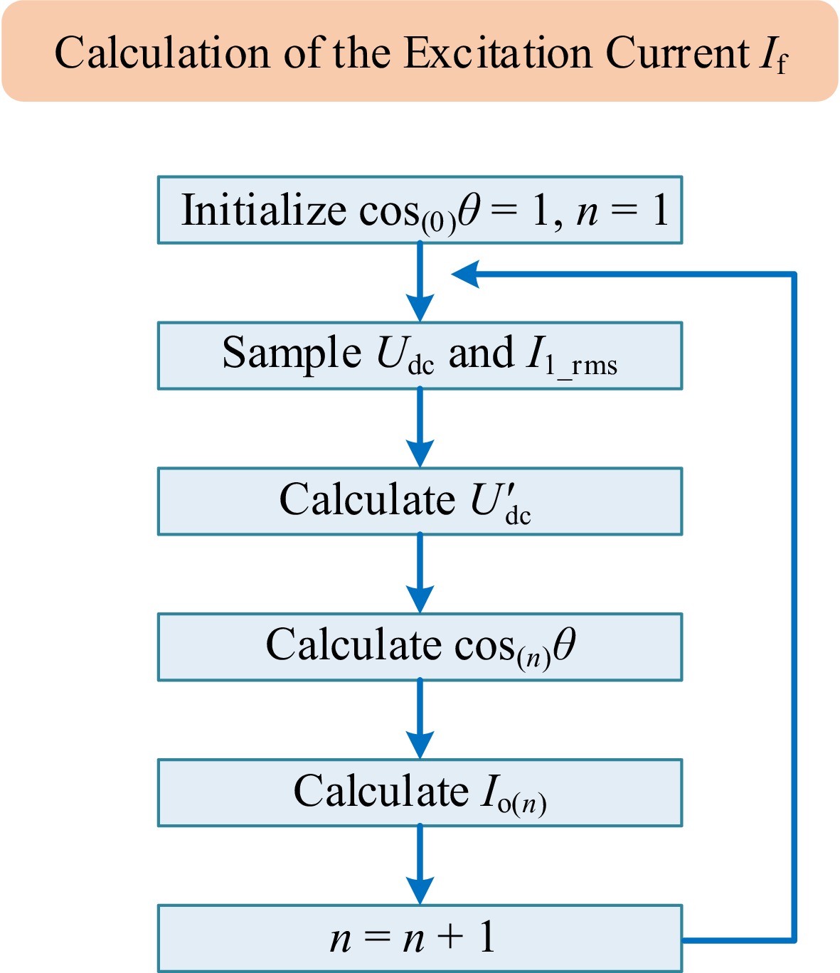
Figure 11.
Block diagram of excitation-current calculation.
Sensitivity analysis of approach 1 with respect to key parameters
-
When the coil parameters or the resonant-capacitor values deviate from their nominal settings, the system becomes detuned. The estimation algorithm’s performance under such detuned conditions must also be evaluated.
As noted above, a comprehensive evaluation of the algorithm’s performance requires assessing its sensitivity to variations in key parameters (LP, LS, and M) as well as sensor accuracy.
The corrected expression for the magnetizing-current estimation is given by:
$ {I_{\text{f}}} = \dfrac{{2\sqrt 2 }}{{\text{π }}}\frac{M}{{{L_{\rm S}}}}{I_{{\text{1\_rms}}}}\cos \left( {\arcsin \dfrac{{U_{\rm{dc}}^{'}{L_{\rm S}}}}{{4\sqrt 2 f{M^2}{I_{{\text{1\_rms}}}}}}} \right) $ (16) From the expression, it can be seen that the magnetizing-current output is influenced by M, LS, I1_rms, Udc, and the operating frequency f. When LP and CP vary, the system’s resonance is disrupted, thereby affecting the performance of the estimation algorithm. Accordingly, the impact of variations in these parameters on the estimation results must be assessed.
All variables were normalized to the base values listed in Table 1, and the voltage and current measurements were likewise normalized using their simulation-derived reference values. To emulate detuning arising from parameter deviations, the normalization coefficient α was swept from 0.90 to 1.10 in simulation, and the influence of sensor measurement noise on the estimation algorithm was evaluated. The resulting estimation errors as functions of the parameters are presented in Fig. 12.
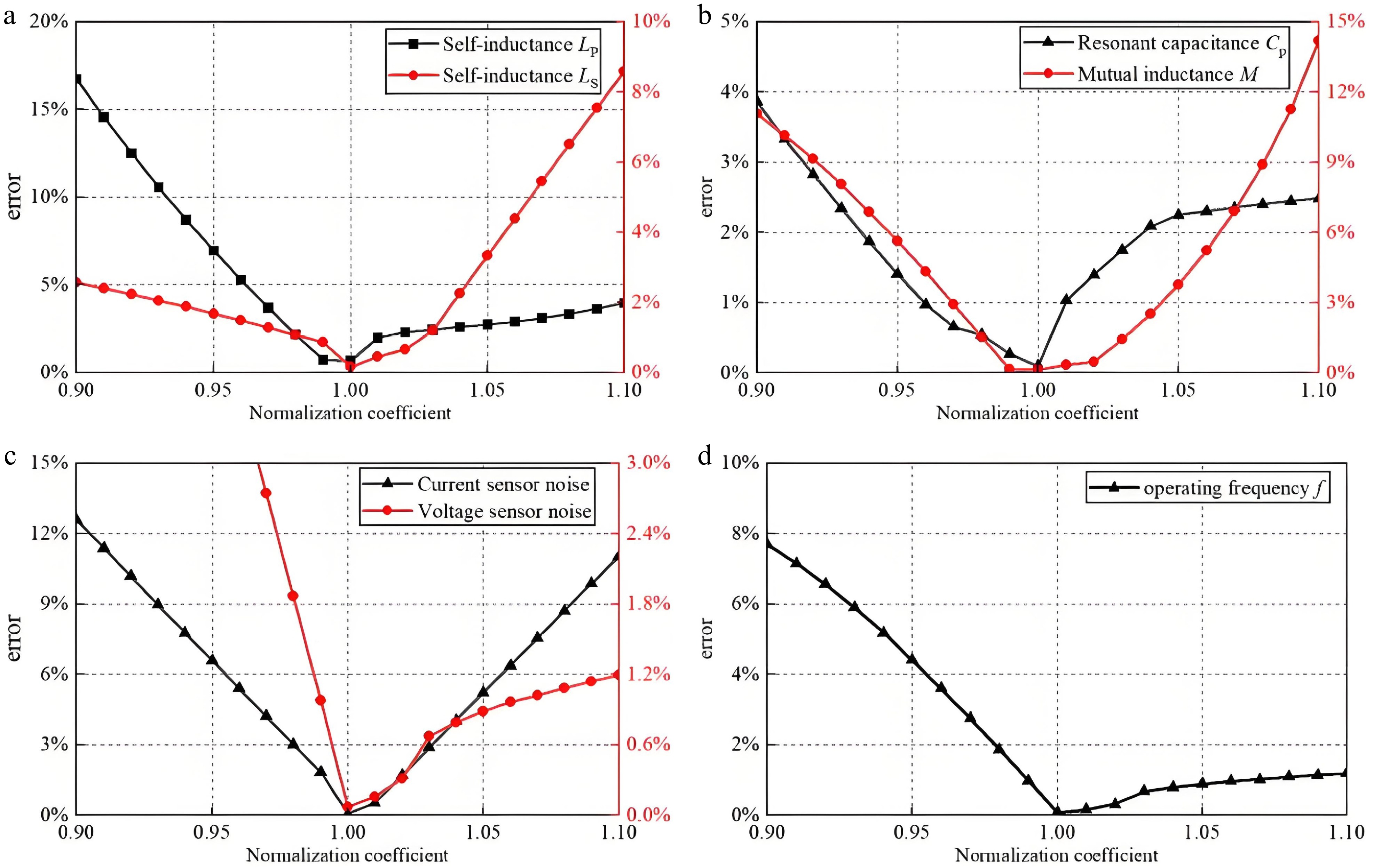
Figure 12.
Estimation error under different parameter-normalization variations (0.90–1.10). (a) Self-inductance LP and LS. (b) Resonant capacitance CP and mutual inductance M. (c) Current and voltage sensor noise. (d) Operating frequency f.
As shown in Fig. 12a, over α ϵ [0.90,1.10] the estimation error varies markedly more with LP than with LS, indicating higher sensitivity to LP; when α ϵ [0.96,1.06], the error does not exceed 5%. For the resonant capacitor CP (Fig. 12b), the estimation error remains below 4% across α ϵ [0.90,1.10], reflecting low sensitivity to CP. By contrast, the error exhibits a larger spread with respect to the mutual inductance M, though it can still be kept within 5% when α ϵ [0.96,1.06]. Regarding sensor accuracy (Fig. 12c), the voltage-sensor error is no more than 3% for α ϵ [0.90,1.10], whereas the current-sensor error satisfies the 5% bound only within the narrower interval α ϵ [0.96,1.04]. This indicates that the algorithm is more sensitive to current-measurement accuracy, while voltage-sensor specifications may be moderately relaxed to reduce cost without compromising overall performance. Finally, Fig. 12d shows that the error remains within 5% for α ϵ [0.94,1.10].
In summary, the estimation algorithm is highly sensitive to the coupling-mechanism parameters and to current-sensor noise; nevertheless, when the normalization coefficient α ϵ [0.95,1.05], the estimation error remains within 5%. By contrast, the algorithm exhibits low sensitivity to the resonant capacitor and to voltage-sensor noise, resulting in only a minor impact on overall performance. In practical deployments, the coupling mechanism is rigidly mounted on the motor shaft, so its relative position is essentially fixed; the magnetic core further mitigates external perturbations, rendering the coupling parameters effectively constant during operation. Moreover, datasheet specifications for typical current sensors generally report noise levels below 5%. Taken together, these findings indicate that the proposed excitation-current estimation algorithm achieves high-accuracy current prediction.
-
To verify the accuracy of the analysis on the characteristics of the S-N resonant topology and the excitation current estimation algorithm in the previous section, an experimental platform for the S-N topology wireless excitation system was established, as shown in Fig. 13. The parameters are the same as those in Table 2. The platform consists of ten main components: rotary magnetic coupler, EESM, current probe, voltage probe, DC power supply, the primary circuit, DSP and emulator, upper computer, and oscilloscope. Specifically, the primary circuit includes a buck converter, high-frequency inverter, resonant capacitors, and sampling circuit. The control program is uploaded from the upper computer to the DSP via the emulator. By adjusting the target value of excitation current on the upper computer, closed-loop control of the excitation current is achieved.
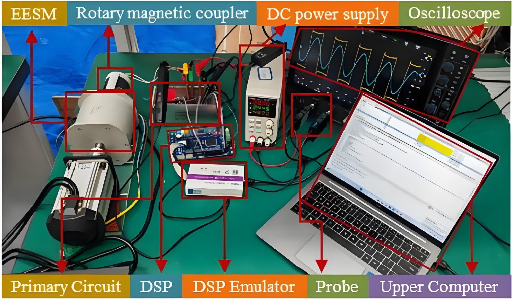
Figure 13.
Experimental platform for the S-N compensated wireless excitation system.
Voltage, current, and ZVS soft-switching results at the primary side
-
The experimental results demonstrate that the high-frequency inverter output voltage u1 exhibits a periodic square waveform, while the primary current i1 presents a sinusoidal waveform, as shown in Fig. 14a. Notably, a distinct phase difference (power angle θ) exists between u1 and i1, which enables zero-voltage switching (ZVS) operation of the MOSFETs. Figure 14b shows the waveform of MOSFET ZVS soft switching. Before the arrival of the driving signal uGS, the voltage uDS has already dropped to zero, which reduces the switching loss of the system.
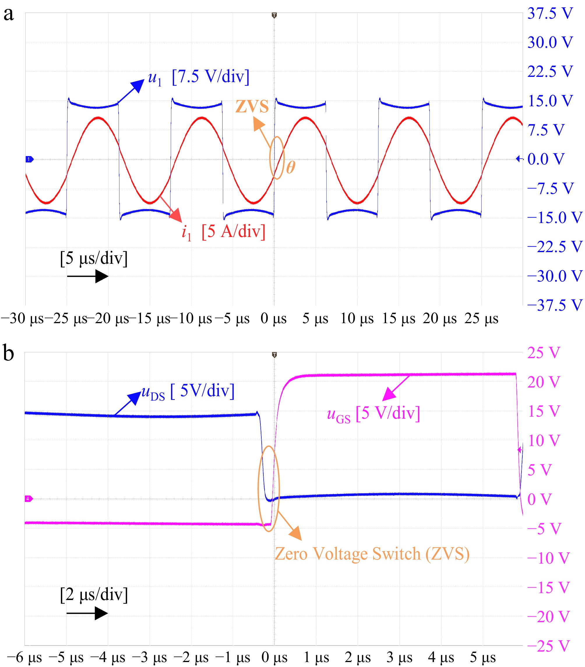
Figure 14.
Waveform diagrams of voltage u1, current i1 and the MOSFET ZVS soft switching. (a) Waveform diagrams of voltage u1 and current i1. (b) Waveform of MOSFET ZVS soft switching.
Verification of the estimation algorithm and the results of closed-loop control
-
To validate the accuracy of the current estimation algorithm, tests were conducted by continuously adjusting the excitation current target value and observing the corresponding variations in the actual excitation current. Experimental results shown in Fig. 15 demonstrate that during the transition process where the excitation current target value increases from 1A to 4A with a step size of 1A and then decreases from 4A to 1A with a step size of 1A, the actual excitation current can effectively track the changes of the target value.
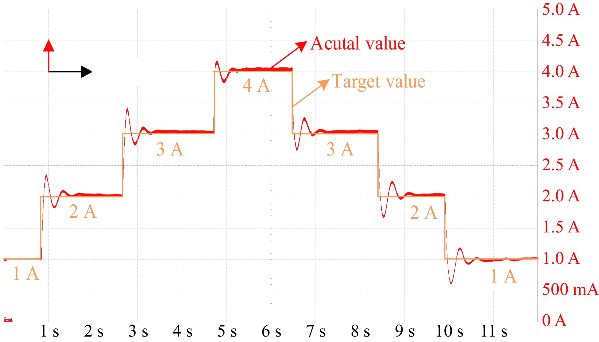
Figure 15.
The waveform of actual excitation current vs target value variation.
Further analysis was performed by calculating the steady-state mean values of the excitation current under different target values, with the quantitative results presented in Table 3. The data indicate that the excitation current estimation algorithm achieves satisfactory accuracy across various target values, with a maximum estimation error of 2.4%. Notably, the estimation error becomes more pronounced at lower setpoints, which can be attributed to the current magnitude falling outside the optimal measurement range of the Hall current sensor, resulting in relatively larger measurement errors under these operating conditions.
Table 3. Error analysis of the current estimation algorithm.
Target value Steady-state mean value Error 1 A 0.976 A 2.4% 2 A 2.008 A 0.4% 3 A 3.004 A 0.13% 4 A 4.006 A 0.15% -
This paper presents a comprehensive solution for excitation current estimation in strongly coupled wireless excitation systems based on the S-N resonant topology. It reveals the calculation principle of excitation current under the S-N topology: the excitation current is determined through the input voltage of the high-frequency inverter Udc, the RMS value of the primary current I1_rms, and the power angle θ. The calculation can be performed using either tanθ or cosθ, while the θ can be obtained through two methods: a calculation method and a sampling method. Based on these different calculation equations and power angle acquisition methods, five distinct estimation approaches are derived.
Simulations were conducted to compare the performance of the five approaches, including the accuracy and reliability of calculations using cosθ and tanθ, the accuracy of power angles obtained through the calculation method and sampling method, and the estimation accuracy of the five distinct approaches. Through these comparisons, approach 1 (Udc, I1_rms, and cosθ) was shown to overcome the limitations of traditional methods, eliminate the need for high-frequency phase detection, and exhibit higher precision, simpler implementation, and stronger load robustness. Sensitivity analysis of approach 1 indicates greater sensitivity to LP and M, with relative insensitivity to CP and voltage-sensor noise; corresponding parameter-tolerance and sensor-selection guidelines are provided. Finally, an experimental platform was constructed for verification. The proposed approach achieves accurate current estimation with a maximum error of only 2.4%.
This work was supported by National Natural Science Foundation of China under Grant No. 52177036, and the Education department of Heilongjiang province under Grant No. LJYXL2022-053.
-
The authors confirm their contributions to the paper as follows: conceptualization: Song B, Ren S, Cui S; methodology, writing original draft preparation: Song B, Ren S; principle analysis: Ren S; platform construction and experimental testing: Ren S, Shi S; funding acquisition, writing review and editing: Cui S, Song B, Dong S; validation: Ren S, Shi S; project administration: Song B, Qi S. All authors have read and agreed to the published version of the manuscript.
-
The data presented in this study are available on request from the corresponding author due to the funder's privacy policy.
-
The authors declare that they have no conflict of interest.
- Copyright: © 2026 by the author(s). Published by Maximum Academic Press, Fayetteville, GA. This article is an open access article distributed under Creative Commons Attribution License (CC BY 4.0), visit https://creativecommons.org/licenses/by/4.0/.
-
About this article
Cite this article
Song B, Ren S, Cui S, Dong S, Shi S, et al. 2026. Design of excitation current estimation algorithm for wireless excitation system of electrically excited motors based on S-N resonant topology. Wireless Power Transfer 13: e005 doi: 10.48130/wpt-0025-0034 

Design of excitation current estimation algorithm for wireless excitation system of electrically excited motors based on S-N resonant topology
- Received: 27 July 2025
- Revised: 30 September 2025
- Accepted: 10 November 2025
- Published online: 02 February 2026
Abstract: Although wireless excitation improves the reliability of electrically excited synchronous motors (EESMs), the rotor field current cannot be directly measured due to the rotation of the rotor. Using the widely adopted S-N topology as a representative framework, this paper reveals the prediction principle of excitation current and proposes five distinct excitation current estimation methods. By comprehensive comparison, the method of estimating the excitation current using the input voltage and the RMS value of the primary current exhibits excellent characteristics across all aspects. It eliminates the need for high-frequency phase detection, is robust to load variation, and provides a reliable technical solution for the closed-loop control of wireless excitation systems. Sensitivity analysis shows that, within a normalized sweep of 0.90–1.10, the estimation error remains within an engineering-acceptable range, providing tolerance-setting and sensor-selection guidance. Experimental validation on an 80 kHz prototype achieves primary-side ZVS, and a maximum steady-state error of 2.4% over 1–4 A setpoints, demonstrating effectiveness and practical feasibility.