


-
With the introduction of concepts such as intelligent manufacturing and industrial Internet, the automatic guided vehicle (AGV), as a representative of modern industrial robots, has gradually developed into an indispensable part of modern production systems.
AGVs are typically powered by batteries. When the battery power is low, the equipment will automatically return to the charging station along the pre-determined route, and the charging head is plugged in manually. This reduces the level of automation and intelligence of the AGV production system. In addition, frequent plugging and unplugging of the charging head in the wired charging mode not only accelerates the aging and wear of the interface but may also cause safety hazards such as electric sparks.
Wireless power transmission (WPT) enables contactless charging[1], which can effectively address the drawbacks associated with the wired charging method for automated guided vehicles (AGVs) mentioned above. At present, this technology has been extensively adopted in diverse fields such as electric vehicles (EV)[2−4], unmanned underwater vehicles (UUV)[5,6], unmanned aircraft systems (UAS)[7], and active implantable medical devices (AIMD)[8,9]. The integration of WPT technology into AGVs can replace manual charging processes and achieve full automation, thereby significantly boosting the operational efficiency of smart production and eliminating the potential safety hazards caused by traditional wired charging[10].
In the static one-on-one charging mode of the WPT system, the offset between the transmitting side (Tx), and the receiving side (Rx) of the system will affect the output power and efficiency. Therefore, research on anti-offset performance has become increasingly important. At present, the anti-offset performance of WPT systems can be enhanced through multiple approaches, such as optimizing control strategies, adjusting compensation topologies, developing novel magnetic coupling mechanisms, and refining system parameters.
Researchers have proposed a closed-loop control system for WPT, which achieves impedance mismatch correction via an additional reactive power compensation circuit, thereby boosting anti-offset capability[11]. A fractional-order WPT system has also been presented, enabling constant voltage (CV), or constant current (CC) output by regulating the system's operating frequency when coil misalignment occurs[12]. Another study introduced a WPT system with bilateral variable inductance control, where output current and voltage are controlled by adjusting inductance values to effectively realize anti-misalignment performance[13]. Additionally, a multivariable control strategy has been developed, utilizing the optimal combination of all control variables to adjust output power with maximum transmission efficiency even in the presence of coil misalignment and load variations[14]. Based on the above studies, current closed-loop control WPT systems require control units to execute complex control strategies and related calculations. Additional secondary and primary side communication components increase the system's cost and design complexity. Therefore, this paper does not adopt the closed-loop control method to enhance the system's resistance to offset.
An innovatively designed magnetic coupling mechanism for WPT systems has been developed, and its ability to alter the magnetic field distribution allows for enhanced anti-misalignment performance of the system. One proposed solution is an array-based transmitting coil configuration: through mutual compensation between the coils in the array, a uniform magnetic field is formed, which in turn boosts the system's anti-offset capability[15]. Another study presents a static wireless charging system equipped with two independent receiving coils; this system can automatically identify and select the coil with the strongest coupling for power transmission, thus improving its misalignment tolerance[16]. Additionally, an asymmetric magnetic coupling mechanism has been put forward, which integrates a third coil to maintain stable power output and transmission efficiency. Notably, this mechanism exhibits favorable longitudinal anti-offset performance without relying on complex control strategies[17]. The new magnetic coupling mechanism can improve the anti-offset performance to a certain extent, but the overall working characteristics of the system are difficult to meet the actual production requirements.
By optimizing and improving the compensation topology, not only can the anti-offset performance of the WPT system be enhanced when the transmitting and receiving coils are offset, but also diversified working characteristics can be achieved. The concept of hybrid topology was first proposed by combining the S-S compensation topology with the LCC-LCC compensation topology, achieving constant current (CC) output characteristics under misalignment conditions[18]. However, when the receiving coil is completely removed, and the system operates in a weak coupling state, the problem of excessive current at the transmitting end arises. To address this issue, a modified hybrid topology has been developed, which not only maintains CC output characteristics under misalignment but also eliminates the excessive current increase at the transmitting end in the weak coupling state[19]. A hybrid topology equipped with a reconfigurable rectifier is proposed, achieving both constant voltage and constant current output independent of the load[20]. Based on the above research, a properly designed hybrid topology structure can further enhance the system's resistance to offset and achieve the required working characteristics that meet actual needs, but it also increases the difficulty of parameter design.
Therefore, optimizing the design of system parameters is of great significance. A parameter design method based on the 'T-type-serial (T-S)' topology is proposed, which can maintain a stable output current when the transmission distance and load of AGV wireless charging change[21]. By optimizing the design parameters of the inverted arch-shaped coil—a structure with unequal winding spacing—using genetic algorithms, the system achieves significantly enhanced misalignment tolerance[22].
At present, extensive research has been conducted on the anti-offset performance of AGV wireless charging, but the studies have often been limited to a single method. In the latest research, it has gradually expanded to the collaborative optimization of multiple methods. A novel quadrature coil structure, integrated with an LCC-S compensation topology is proposed. Through an optimized parameter design, the system achieves markedly improved misalignment tolerance without the need for complex control[23]. However, although the anti-offset capabilities of both the X- and Y-axis have been enhanced, the voltage fluctuations remain relatively large. A reconfigurable hybrid topology WPT system has been demonstrated for battery CC-CV charging with good misalignment tolerance. However, its practical adoption in AGVs is hindered by computational complexity in parameter design, and a costly control system[24]. While the co-optimization of multiple methods yields favorable results for enhancing misalignment tolerance, the design process becomes correspondingly complex. Given that the navigation systems of AGVs (e.g., laser, electromagnetic, or braking slots) inherently constrain their movement, the required misalignment tolerance may not be symmetric in the X- and Y-axes. By prioritizing the tolerance in a specific primary axis of movement, the design process can be significantly simplified while still fulfilling practical requirements.
Based on the existing literature research, this paper adopts a hybrid topology to construct a static one-to-one wireless charging system for AGVs, and designs a matching magnetic coupling mechanism. Through a reasonable parameter design method, the integration degree of multiple methods is further improved, thereby enhancing the system's anti-offset capability in a single direction. Among them, the forward and backward directions of the AGV are defined as the X-axis direction, its left and right sides are defined as the Y-axis direction, and the direction perpendicular to the XOY plane is defined as the Z-axis direction.
-
To achieve load-independent constant voltage (CV) output characteristics, and ensure that the output voltage of the coil remains relatively stable within a certain offset range, this paper proposes a hybrid topology structure. This structure combines the CLC-S compensation topology with the S-CLC compensation topology to form a serial-in-parallel-out hybrid topology architecture. The circuit schematic of the one-to-one wireless charging system for AGVs based on this structure is shown in Fig. 1.
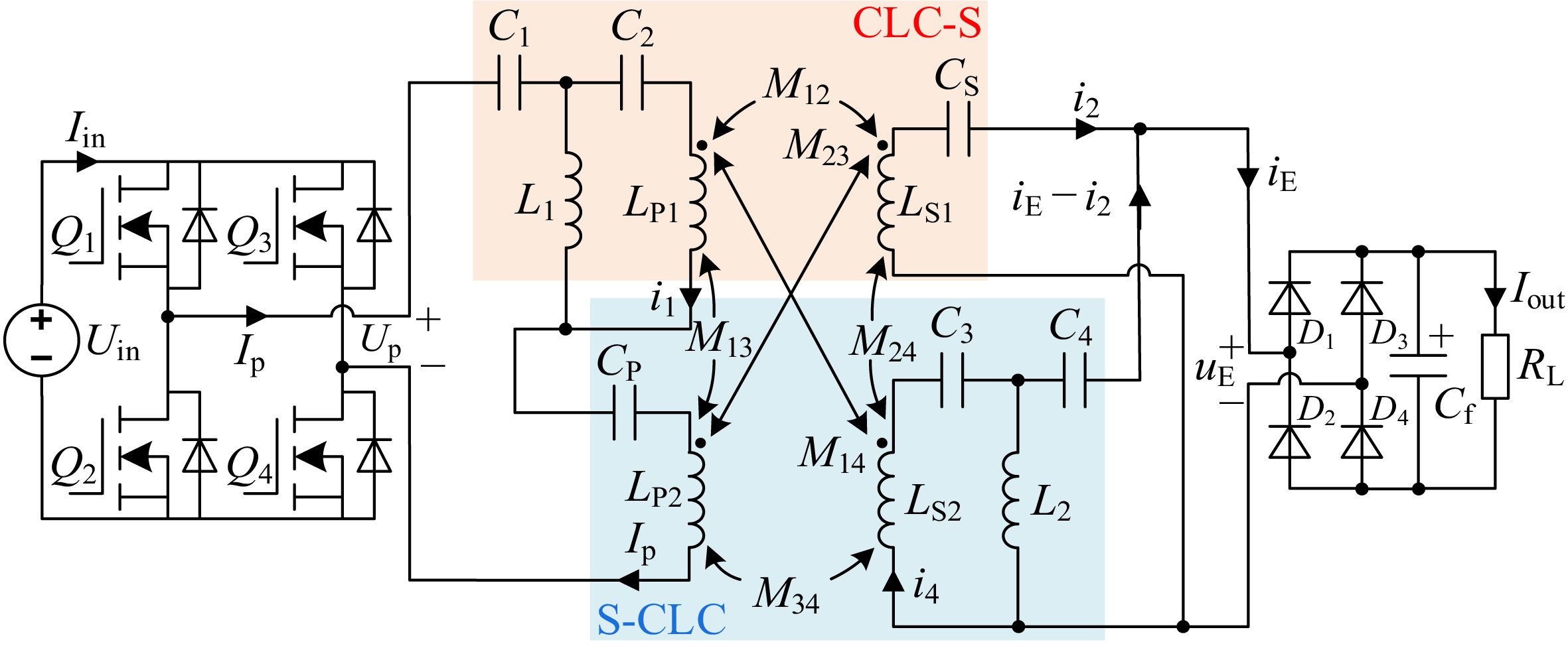
Figure 1.
Schematic circuit diagram of the WPT system with hybrid topology.
To clarify the key components and parameters of the proposed WPT system, the definitions are as follows: Q1~Q4 are MOSFETs configured in a full-bridge topology to form the inverter. D1~D4 serve as the four rectifier diodes, and RL denotes the load resistance. For inductive components, L1 and L2 represent the self-inductances of the two compensation inductors, while LP1, LP2, LS1, and LS2 correspond to the self-inductances of transmitting coil 1 (Tx1), transmitting coil 2 (Tx2), receiving coil 1 (Rx1), and receiving coil 2 (Rx2) respectively. The capacitive elements include C1, C2, C3, C4, CP, and CS (all acting as compensation capacitors), as well as Cf (a filter capacitor). Regarding mutual inductances, M12 and M34 refer to the mutual inductances between Tx1 & Rx1, and Tx2 & Rx2, respectively—these are defined as the main mutual inductances since they provide the essential inductive coupling required for the system's operation. In contrast, M13, M14, M23, and M24 are the mutual inductances between Tx1 & Tx2, Tx1 & Rx2, Tx2 & Rx1, and Rx1 & Rx2; these are classified as cross-coupling mutual inductances as they arise from cross-coupling effects between the coils. For voltage parameters, Uin is the input DC voltage, Up is the AC voltage output by the inverter, and uE is the AC voltage input to the rectifier. As for current parameters, Iin is the input DC current, Ip is the AC current output by the inverter, i1, i2, and i4 are the AC currents flowing through Tx1, Rx1, and Rx2 respectively, and Iout is the output DC current.
By applying the fundamental harmonic approximation method, this paper establishes the equivalent circuit of the proposed hybrid topology WPT system, as shown in Fig. 2.
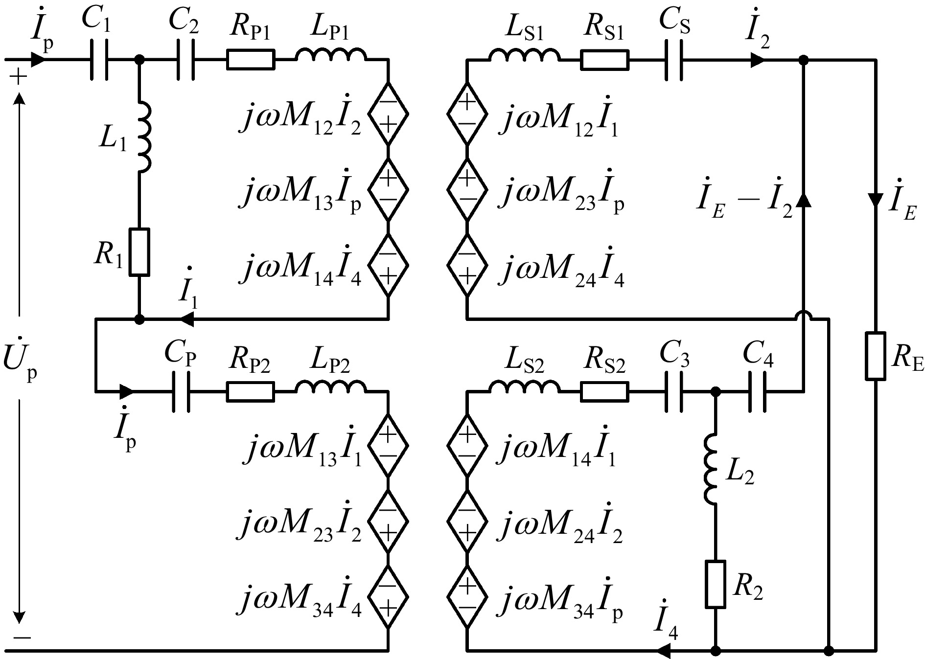
Figure 2.
The equivalent circuit model of the WPT system with a hybrid topology.
Voltages and currents are expressed in phasor form, while the mutual coupling between Tx1/Tx2, and Rx1/Rx2 is modeled by equivalent controlled sources. Additionally, assuming the rectifiers are lossless at their terminals, the equivalent resistance RE can be written as:
$ {R}_{\text{E}}=8{R}_{\text{L}} / {\text{π}}^{2} $ (1) Let the angular frequency of the system be ω, and the corresponding operating frequency is f (ω = 2πf). By combining the equivalent circuit shown in Fig. 2 and applying Kirchhoff's laws, Eq. (2) can be established:
$ \begin{split}&\qquad\qquad\qquad\qquad\qquad\qquad\qquad\begin{bmatrix} \dot{U}_{\mathrm{p}} \\ \dot{U}_{\mathrm{p}} \\ 0 \\ 0 \\ 0 \end{bmatrix} = \\ &{\begin{bmatrix} Z_1 + Z_{{\mathrm{P}}2} + j\omega M_{13} & Z_2 + j\omega M_{13} & -j\omega(M_{12} + M_{23}) & -j\alpha(M_{14} + M_{34}) & 0 \\ Z_1 + Z_{{\mathrm{P}}1} + Z_{{\mathrm{P}}2} & -Z_{{\mathrm{P}}1} + j\omega M_{13} & -j\omega M_{23} & -j\omega M_{34} & 0 \\ -j\omega M_{23} & -j\omega M_{12} & Z_{S1} & j\omega M_{24} & R_{\mathrm{E}} \\ -j\omega M_{34} & -j\omega M_{14} & -Z_4 + j\omega M_{24} & Z_3 & Z_4 + R_{\mathrm{E}} \\ 0 & 0 & -Z_{S2} - Z_4 & -Z_{S2} & Z_{S2} + Z_4 + R_{\mathrm{E}} \end{bmatrix}}\\ &\qquad\qquad\qquad\qquad\qquad\qquad\qquad\begin{bmatrix} {{{\dot I}_{\text{p}}}} \\ {{{\dot I}_1}} \\ {{{\dot I}_2}} \\ {{{\dot I}_4}} \\ {{{\dot I}_{\text{E}}}} \end{bmatrix} \\[-1pt]\end{split}$ (2) The symbols in Eq. (2) are defined as follows: Up denotes the AC voltage across the inverter, while Ip, I1, I2, I4, and IE represent the AC currents flowing through the inverter, Tx1, Rx1, Rx2, and the rectifier, respectively. Additionally, the impedances involved in Eq. (2) are given by:
$ \begin{cases} {Z}_{1}=1 / \left(j\omega {C}_{1}\right),\;{Z}_{2}=j\omega {L}_{\text{P1}}+1 / \left(j\omega {C}_{2}\right)+{R}_{\text{P1}}\\ {Z}_{3}=j\omega {L}_{\text{S2}}+1 / \left(j\omega {C}_{3}\right)+{R}_{\text{S2}},\;{Z}_{4}=1 / \left(j\omega {C}_{4}\right)\\ {Z}_{\text{P1}}=j\omega {L}_{1}+{R}_{1},\;{Z}_{\text{P2}}=j\omega {L}_{\text{P2}}+1 / \left(j\omega {C}_{\text{P}}\right)+{R}_{\text{P2}}\\ {Z}_{\text{S1}}=j\omega {L}_{\text{S1}}+1 / \left(j\omega {C}_{\text{S}}\right)+{R}_{\text{S1}},\;{Z}_{\text{S2}}=j\omega {L}_{2}+{R}_{2} \end{cases} $ (3) The impedance terms are defined as follows: Z1, Z4, ZP1, ZS2 for C1, C4, L1, L2; Z2, Z3, ZP2, ZS1 for the combined impedances of (Tx1 + C2), (Rx2 + C3), (Tx2 + CP), (Rx1 + CS); and R1, R2, RP1, RP2, RS1, RS2 as the parasitic resistances of L1, L2, Tx1, Tx2, Rx1, Rx2.
Operating in the resonant state, the hybrid-topology WPT system has a corresponding angular frequency of ω0 = 2πf0. This means that both constituent topologies — CLC-S and S-CLC — are individual in resonance. The system's resonant condition is given by:
$ \begin{cases} {Z}_{1}+{Z}_{\text{P}1}=0,\;{Z}_{1}-{Z}_{2}=0\\ {Z}_{4}+{Z}_{\text{S2}}=0,\;{Z}_{4}-{Z}_{3}=0 \end{cases} $ (4) By substituting Eqs. (3) and (4) into Eq. (2), ignoring all parasitic resistances and cross-coupling mutual inductances, and retaining only the main mutual inductances M12 and M34, the following expressions for the currents can be obtained:
$ \left\{\begin{aligned} & {\dot{I}}_{\text{p}}=\dfrac{{\dot{U}}_{\text{p}}{M}_{12}{}^{2}{L}_{2}{}^{2}}{{R}_{\text{E}}{({{L}_{1}}{{L}_{2}}+{{M}_{12}}{{M}_{34}})}^{2}},\;{\dot{I}}_{1}=\dfrac{j{\dot{U}}_{\text{p}}{L}_{2}}{{\omega }_{0}({L}_{1}{L}_{2}+{M}_{12}{M}_{34})}\\ & {\dot{I}}_{2}=-\dfrac{{\dot{U}}_{\text{p}}{M}_{12}{L}_{1}{L}_{2}{}^{2}}{{R}_{\text{E}}{({{L}_{1}}{{L}_{2}}+{{M}_{12}}{{M}_{34}})}^{2}},\;{\dot{I}}_{4}=\dfrac{j{\dot{U}}_{\text{p}}{M}_{12}}{{\omega }_{0}({L}_{1}{L}_{2}+{M}_{12}{M}_{34})}\\ & {\dot{I}}_{\text{E}}=-\dfrac{{\dot{U}}_{\text{p}}{M}_{12}{L}_{2}}{{R}_{\text{E}}({L}_{1}{L}_{2}+{M}_{12}{M}_{34})} \end{aligned}\right. $ (5) The output voltage gain GVV of the proposed WPT system with a hybrid topology can be obtained from Eq. (5) as follows:
$ G\text{VV}=\left| {\dot{I}}_{\text{E}}{R}_{\text{E}} / {\dot{U}}_{\text{p}}\right| \text=\dfrac{{M}_{12}{L}_{2}}{{L}_{1}{L}_{2}+{M}_{12}{M}_{34}}\text=\dfrac{1}{{L}_{1} / {M}_{12}+{M}_{34} / {L}_{2}} $ (6) It can be seen from Eq. (6) that the voltage gain GVV of the system is independent of the load resistance RE, achieving a constant voltage (CV) output characteristic independent of the load, and it is respectively proportional and inversely proportional to the two main mutual inductances M12 and M34. When the offset occurs, M12 and M34 will gradually decrease, in which the decrease of M34 will increase GVV, and the decrease of M12 will decrease GVV, and GVV's stability depends on the parameter design of L1 and L2. At the same time, it is noted that when in the weak coupling state, M12 and M34 are about zero, and GVV is about zero, and only i1 has a certain numerical value. There is no overvoltage or overcurrent problem, and the system safety is guaranteed.
The input impedance of the system can also be obtained from Eq. (5), which can be expressed as:
$ {Z}_{\text{in}}={\dot{U}}_{\text{p}} / {\dot{I}}_{\text{p}}\text={R}_{\text{E}}{({{L}_{1}}{{L}_{2}}+{{M}_{12}}{{M}_{34}})}^{2} / \left({M}_{12}{}^{2}{L}_{2}{}^{2}\right) $ (7) As indicated by Eq. (7), achieving resonance in the proposed WPT system results in a purely resistive input impedance, thereby satisfying the requirement for a zero-phase-angle (ZPA) input.
This hybrid topology structure mainly takes advantage of the real-time superposition characteristics of the two energy transmission paths within the system to provide compensation when the coil shifts, thereby enhancing the system's resistance to shift. This hybrid topology structure is fundamentally different from the hybrid topology structure that adopts a switching mode. This mechanism fundamentally provides smoother and more robust anti-shift performance because it does not have discrete switching actions and potential switching transient issues.
-
The analysis of the characteristics of the hybrid topology is based on the assumption of retaining only the main mutual inductance. Therefore, the design and selection of the coils need to be such that the cross-coupling mutual inductance can be minimized as much as possible. To completely eliminate all cross-coupled mutual inductances (M13, M14, M23, and M24), this paper proposes a novel self-decoupling magnetic coupling mechanism termed the 'self-decoupling cross-shaped coil'. The coil is uniformly wound on the cross-shaped ferrite along two mutually perpendicular directions (X- and Y-axis) by means of orthogonal winding technology. The coil is uniformly wound with the lines on the cross-shaped ferrite in two mutually perpendicular directions (the X-axis direction and the Y-axis direction) through orthogonal winding, as shown in Fig. 3. Among them, the transmitting coil Tx is composed of the transmitting coils Tx1 and Tx2 wound orthogonally, and the receiving coil Rx is composed of the receiving coils Rx1 and Rx2 wound orthogonally. The cross-shaped ferrite in the transmitting and receiving coils are all 159 mm × 159 mm × 10 mm in size. All the coils are wound with 19 turns using the Leeds wire with a specification of 300 × 0.12 mm. The winding direction of the coils is indicated by red arrows. The winding directions of Tx1 and Rx1 are the same, and those of Tx2 and Rx2 are also the same. In addition, the distance between the Rx ferrite and the Tx ferrite is defined as the transmission distance h.
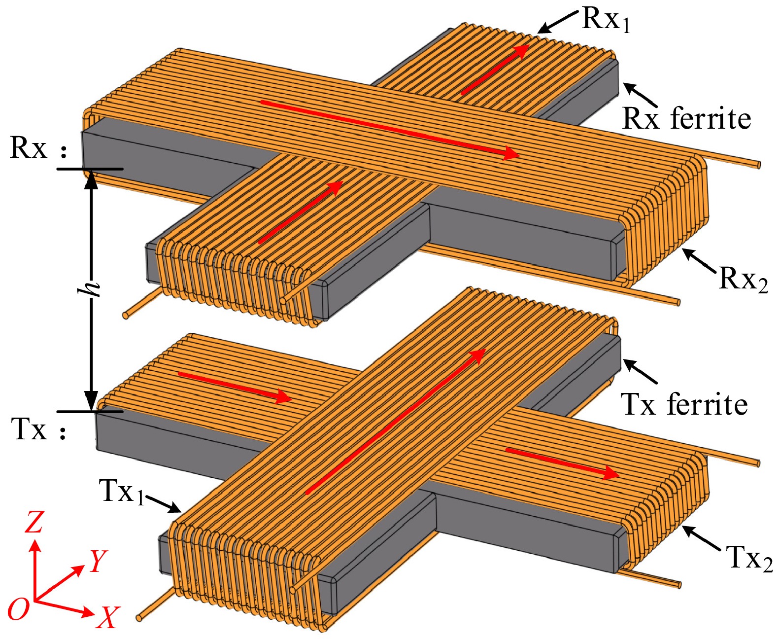
Figure 3.
Self-decoupling cross coil.
The decoupling characteristics of the proposed self-decoupled cross coil are analyzed using the Neumann formula. Its calculation formula is as follows:
$ {M}_{ij}=\dfrac{{\mu }_{0}{N}_{i}{N}_{j}}{4\text{π}}\oint \oint \dfrac{\text{d}{\boldsymbol{L}}_{i}\cdot \text{d}{\boldsymbol{L}}_{\boldsymbol{j}}}{{R}_{\boldsymbol{i}j}} $ (8) where, the mutual inductance Mij describes the electromagnetic coupling between two coils, designated as coil i and coil j. This key parameter depends on the vacuum permeability
$\mu_0 $ From Eq. (8), it can be known that when the winding directions of the coils are perpendicular to each other, the mutual inductance will be zero. Therefore, the mutual inductances of the cross-coupled components M13, M14, M23, and M24, are all zero. And the mutual inductance between the same-direction coupled coils M12 and M34 is not zero. It meets the magnetic coupling mechanism requirements of the WPT system. However, other coils (such as the DD and BP coils) are difficult to directly meet this requirement.
To validate the practical performance of the proposed self-decoupling cross coil, actual measurements were carried out on the coil's self-inductance, all induced mutual inductances, and the coupling coefficient k of the main mutual inductance under X-, Y-, and Z-axis offsets within a specific range. The rated operating position of the self-decoupling cross coil is defined as the state with no X- or Y-axis offset, and the rated transmission distance is set to hN = 45 mm. Subsequently, measurements and analyses were conducted on the self-decoupled cross coil within the range of an 80 mm offset on both the X- and Y-axis, as well as within the Z-axis offset range of −15 to +15 mm.
The self-inductance of the X-axis direction offset measured in the experiment is shown in Fig. 4a. When the lateral offset reaches up to 80 mm, the self-inductance of Tx1, Tx2, Rx1, and Rx2 shows a relatively small drift. Therefore, the self-inductance at the rated working position can be directly used for the system parameter design.
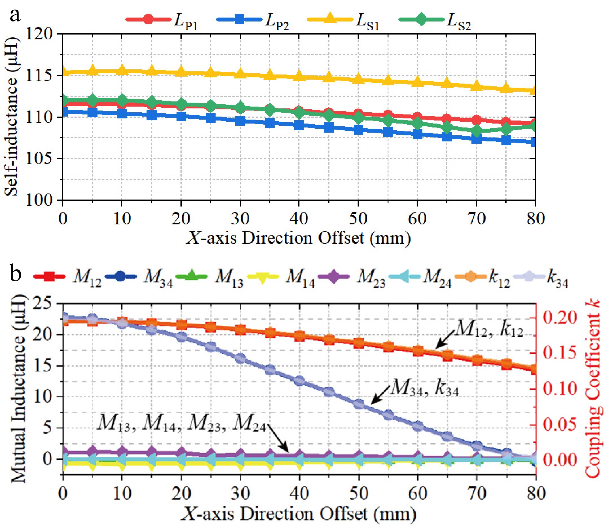
Figure 4.
X-axis direction offset. (a) Self-inductance. (b) Mutual inductance and coupling coefficient k.
The X-axis offset mutual inductance and coupling coefficient k measured in the experiment is shown in Fig. 4b. All cross-coupled mutual inductances M13, M14, M23, and M24 are very small and can be ignored compared with the main mutual inductances M12 and M34. In addition, the reduction rate of M34 is significantly faster than that of the M12, M12N, and M34N are defined as the main mutual inductances at the rated working position, then the main mutual inductances measured in the experiment is M12N = 22.21 μH, and M34N = 22.79 μH. At the maximum offset, the main mutual inductance has the minimum values, which are M12min = 14.35 μH, and M34min = −0.39 μH. Similar to the variation trend of mutual inductance, the coupling coefficient k34 of M34 also decreases significantly faster than that of M12. Among them, the maximum value at the rated working position k12 and k34 are 0.196 and 0.200, respectively. At the maximum offset of 80 mm in the X-axis direction, k12 and k34 have minimum values of 0.129 and 0.004, respectively.
The self-inductance in the Y-axis direction measured in the experiment is shown in Fig. 5a. It can be observed that at the maximum offset of 80 mm in the Y-axis direction, the self-inductance of Tx1, Tx2, Rx1, and Rx2 also show a relatively small drift. Therefore, when there is an offset in the Y-axis direction, directly using the self-inductance at the rated working position for system parameter design.
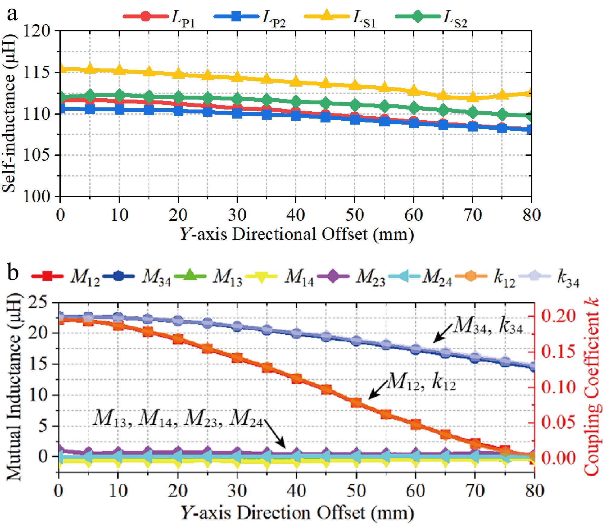
Figure 5.
Y-axis direction offset. (a) Self-inductance. (b) Mutual inductance, and coupling coefficient k.
The mutual inductance and coupling coefficient k in the Y-axis direction measured in the experiment is shown in Fig. 5b. Similar results to those shown in Fig. 4b can be observed. However, contrary to the trend of mutual inductance changes along the X-axis direction, the rate of decrease for M12 is significantly faster than that of M34. It shows a similar trend to the mutual inductance variation. The rate of decrease of the coupling coefficient k12 of M12 is significantly faster than that of k34 of M34.
The Z-axis direction self-inductance measured in the experiment is shown in Fig. 6a. As the transmission distance h increases, the self-inductance of Tx1, Tx2, Rx1, and Rx2 gradually decrease and become more stable. When the transmission distance h is small, it will cause a large self-inductance drift, while when the transmission distance h is large, its influence on the self-inductance will significantly decrease. Therefore, in this paper, hN = 45 mm is selected as the rated transmission distance. Under this transmission distance, the self-inductance drift of the X-axis direction offset, and the Y-axis direction offset is relatively small, which is suitable for directly using the self-inductance of the rated working position for system parameter design, as shown in Figs. 4a and 5a.
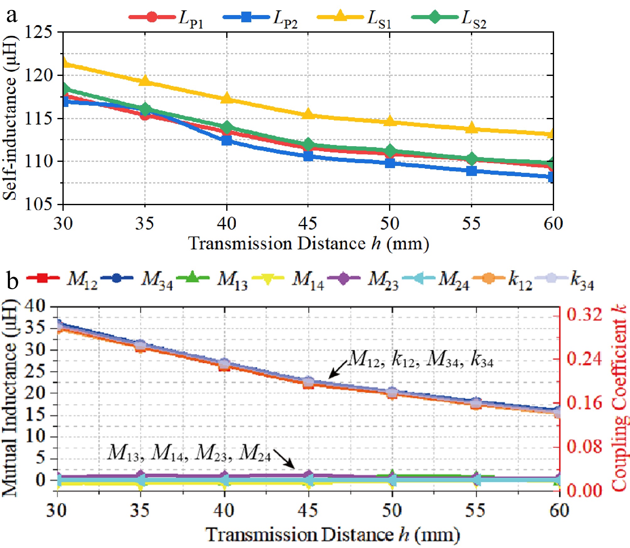
Figure 6.
Z-axis direction offset. (a) Self-inductance. (b) Mutual inductance, and coupling coefficient k.
The mutual inductance and coupling coefficient k in the Z-axis direction measured in the experiment is shown in Fig. 6b. It can be observed that, unlike in Figs. 4b and 5b, when there is a Z-axis direction offset, the trend of changes for M12 and M34 is basically the same, and M12 ≈ M34. It has a similar trend to the mutual inductance variation. At any Z-axis direction offset, k12 is approximately equal to k34.
-
Derived and analyzed from the hybrid topology circuit model, both main inductances will decrease under offset conditions, and their mutual compensation effect helps stabilize the GVV against such offsets. The stability of this compensation relies on the parameters of L1 and L2, thus prompting the proposal of a system parameter optimization approach, and implementation process based on the approximate calculation of the main inductances.
The design basis for L2 parameters
-
In this paper, the voltage fluctuation coefficient δV of the WPT system within the given offset range is defined as:
$ {\delta }_{\text{V}}=\left| {V}_{\text{X}} / \left({V}_{\text{X}}-{V}_{\text{N}}\right)\right| \times 100{\text{% }}\leq \Delta $ (9) where, VX represents the output voltage of the system when it undergoes offset, VN represents the output voltage of the system at the rated working position, and Δ represents the upper threshold of the voltage fluctuation coefficient δV.
The rated voltage gain GVVN defined at the rated operating position is:
$ {G}_{\text{VVN}}=\dfrac{1}{{L}_{\text{1}} / {M}_{\text{12N}}+{M}_{\text{34N}} / {L}_{\text{2}}} $ (10) where, M12N and M34N respectively represent the two main mutual inductances when the rated working position is reached. So, according to Eq. (10), L1 can be expressed by L2:
$ {L}_{\text{1}}={M}_{\text{12N}}({L}_{\text{2}}-{G}_{\text{VVN}}{M}_{\text{34N}}) / \left({G}_{\text{VVN}}{L}_{\text{2}}\right) $ (11) By combining Eqs. (9) and (10), it can be seen that in order to keep the system output voltage fluctuation within the threshold range, the system voltage gain GVV must satisfy the following inequality condition:
$ (1-\Delta ){G}_{\text{VVN}}\leq {G}_{\text{VV}}\leq (1+\Delta ){G}_{\text{VVN}} $ (12) Considering that AGV usually has the guidance of sensors during its movement along the X-axis, the deviation in the Y-axis direction is relatively small. Therefore, this paper mainly improves the anti-offset performance of the WPT system in the X-axis direction. To reduce the design difficulty, the relationship between M12 and M34 can be approximated as a linear function:
$ {M}_{34}=a{M}_{12}+b $ (13) Substituting Eq. (13) into Eq. (6), the system voltage gain GVV can be expressed by M12 as F(M12):
$ F({M}_{\text{12}})=\dfrac{1}{{L}_{\text{1}} / {M}_{\text{12}}+\left(a{M}_{\text{12}}+b\right) / {L}_{\text{2}}} $ (14) To find the inflection point of F(M12) from Eq. (14), set:
$ \dfrac{\text{d}F({M}_{\text{12}})}{\text{d}{M}_{\text{12}}}=0 $ (15) The inflection point of F(M12) is obtained by solving Eq. (15):
$ {M}_{\text{12i}}=\sqrt{{L}_{1}{L}_{2} / a} $ (16) Let M12min and M12max represent the minimum and maximum values of the mutual inductance M12 within the given offset range. From Eqs. (14) and (16), it can be concluded that the relationships between M12min, M12max, and the inflection point M12i may fall into the following four cases, as shown in Fig. 7.
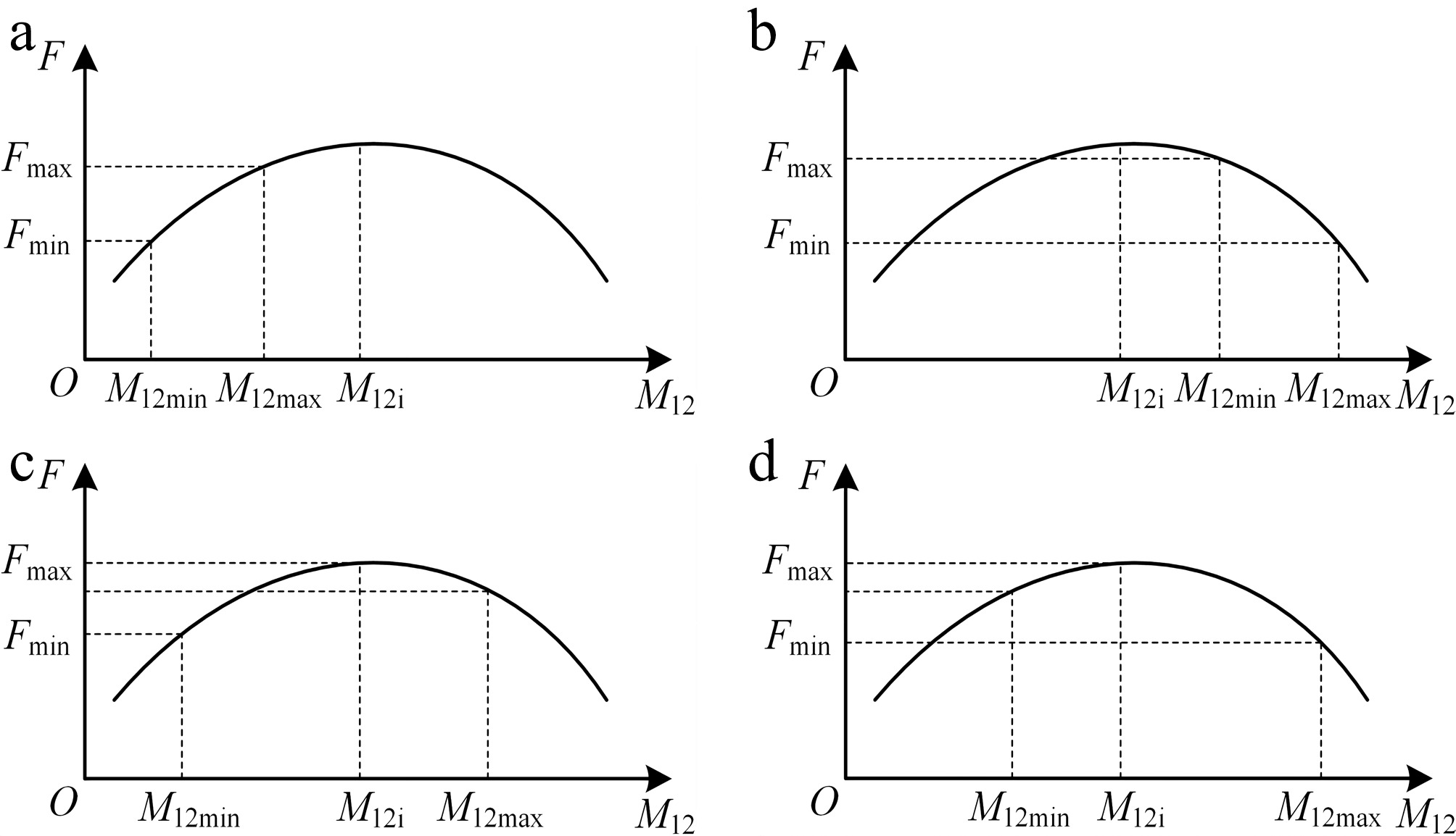
Figure 7.
Curve depicting the relationship between system voltage gain and the primary mutual inductance M12. (a) Monotonically increasing. (b) Monotonically decreasing. (c) Take the minimum value at M12min. (d) Take the minimum value at M12max.
(1) As shown in Fig. 7a, F(M12) is monotonically increasing on the interval [M12min, M12max], and if M12i ≥ M12max, then substituting Eq. (14) into Eq. (12) leads to the inequality system:
$ \begin{cases} \sqrt{{L}_{1}{L}_{2} / a}\geq {M}_{12\max }\\ {L}_{\text{1}} / {M}_{\text{12max}}+{M}_{\text{34max}} / {L}_{\text{2}}\geq 1 / \left[(1+\Delta ){G}_{\text{VVN}}\right]\\ {L}_{\text{1}} / {M}_{\text{12min}}+{M}_{\text{34min}} / {L}_{\text{2}}\leq 1 / \left[(1-\Delta ){G}_{\text{VVN}}\right] \end{cases} $ (17) Substituting Eq. (11) into Eq. (17) yields:
$ \left\{\begin{aligned} & {L}_{2}\geq \left[{G}_{\text{VVN}}(aM_{\text{12max}}^{2}+{M}_{\text{12N}}{M}_{\text{34N}})\right] / {M}_{\text{12N}}\\ & {L}_{2}\geq \dfrac{(1+\Delta ){G}_{\text{VVN}}({M}_{\text{12N}}{M}_{\text{34N}}-{M}_{\text{12max}}{M}_{\text{34max}})}{(1+\Delta ){M}_{\text{12N}}-{M}_{\text{12max}}}\\ & {L}_{2}\leq \dfrac{(1-\Delta ){G}_{\text{VVN}}({M}_{\text{12N}}{M}_{\text{34N}}-{M}_{\text{12min}}{M}_{\text{34min}})}{(1-\Delta ){M}_{\text{12N}}-{M}_{\text{12min}}} \end{aligned}\right. $ (18) (2) As shown in Fig. 7b, F(M12) is monotonically decreasing on the interval [M12min, M12max], and if M12i ≤ M12min, substituting Eq. (14) into Eq. (12) leads to the inequality system:
$ \begin{cases} \sqrt{{L}_{1}{L}_{2} / a}\leq {M}_{12\min }\\ {L}_{\text{1}} / {M}_{\text{12min}}+{M}_{\text{34min}} / {L}_{\text{2}}\geq 1 / \left[(1+\Delta ){G}_{\text{VVN}}\right]\\ {L}_{\text{1}} / {M}_{\text{12max}}+{M}_{\text{34max}} / {L}_{\text{2}}\leq 1 / \left[(1-\Delta ){G}_{\text{VVN}}\right] \end{cases} $ (19) Substituting Eq. (11) into Eq. (19) yields:
$ \left\{\begin{aligned} & {L}_{2}\leq \left[{G}_{\text{VVN}}(aM_{\text{12min}}^{2}+{M}_{\text{12N}}{M}_{\text{34N}})\right] / {M}_{\text{12N}}\\ & {L}_{2}\geq \dfrac{(1+\Delta ){G}_{\text{VVN}}({M}_{\text{12N}}{M}_{\text{34N}}-{M}_{\text{12min}}{M}_{\text{34min}})}{(1+\Delta ){M}_{\text{12N}}-{M}_{\text{12min}}}\\ & {L}_{2}\geq \dfrac{(1-\Delta ){G}_{\text{VVN}}({M}_{\text{12N}}{M}_{\text{34N}}-{M}_{\text{12max}}{M}_{\text{34max}})}{(1-\Delta ){M}_{\text{12N}}-{M}_{\text{12max}}} \end{aligned}\right. $ (20) As shown in Fig. 7c and d, if the inflection point M12i is within the interval range of [M12min, M12max], then by setting M12min ≤ M12i ≤ M12max, we can obtain:
$ \dfrac{{G}_{\text{VVN}}(aM_{\text{12min}}^{2}+{M}_{\text{12N}}{M}_{\text{34N}})}{{M}_{\text{12N}}}\leq {L}_{2}\leq \dfrac{{G}_{\text{VVN}}(aM_{\text{12max}}^{2}+{M}_{\text{12N}}{M}_{\text{34N}})}{{M}_{\text{12N}}} $ (21) Since F(M12) attains its maximum value at the inflection point M12i, substituting Eq. (14) into Eq. (12) yields the inequality:
$ {L}_{\text{1}} / {M}_{\text{12i}}+\left[a{M}_{\text{12i}}+b\right] / {L}_{\text{2}}\geq 1 / \left[(1+\Delta ){G}_{\text{VVN}}\right] $ (22) Substituting Eq. (11) into Eq. (22) yields:
$ \begin{split} & (1+\Delta ){G}_{\text{VVN}}\left[2a\left(1+\Delta \right){M}_{\text{12N}}+b-2\sqrt{{a}^{2}({\Delta }^{2}+2\Delta )M_{12\text{N}}^{2}+ab\Delta {M}_{\text{12N}}}\right]\leq {L}_{2}\\ & \leq (1+\Delta ){G}_{\text{VVN}}\left[2a\left(1+\Delta \right){M}_{\text{12N}}+b+2\sqrt{{a}^{2}({\Delta }^{2}+2\Delta )M_{12\text{N}}^{2}+ab\Delta {M}_{\text{12N}}}\right] \end{split} $ (23) (3) As shown in Fig. 7c, F(M12) attains its minimum value at M12min. Substituting Eq. (14) into Eq. (12) yields:
$ {L}_{\text{1}} / {M}_{\text{12min}}+{M}_{\text{34min}} / {L}_{\text{2}}\leq 1 / \left[(1-\Delta ){G}_{\text{VVN}}\right] $ (24) Substituting Eq. (11) into Eq. (24) yields:
$ {L}_{2}\leq \dfrac{(1-\Delta ){G}_{\text{VVN}}({M}_{\text{12N}}{M}_{\text{34N}}-{M}_{\text{12min}}{M}_{\text{34min}})}{(1-\Delta ){M}_{\text{12N}}-{M}_{\text{12min}}} $ (25) (4) As shown in Fig. 7d, F(M12) attains its minimum value at M12max. Substituting Eq. (14) into Eq. (12) yields:
$ {L}_{\text{1}} / {M}_{\text{12max}}+{M}_{\text{34max}} / {L}_{\text{2}}\leq 1 / \left[(1-\Delta ){G}_{\text{VVN}}\right] $ (26) Substituting Eq. (11) into Eq. (26) yields:
$ {L}_{2}\geq \dfrac{(1-\Delta ){G}_{\text{VVN}}({M}_{\text{12N}}{M}_{\text{34N}}-{M}_{\text{12max}}{M}_{\text{34max}})}{(1-\Delta ){M}_{\text{12N}}-{M}_{\text{12max}}} $ (27) The above discussion and treatment have classified and addressed the four possible cases of the turning points of the function F(M12). Obviously, within the determined maximum offset range, the numerical values of L2 can be calculated through the above inequalities. If the solutions of L2 have intersections, it indicates that L2 exists in this case, and the specific numerical value of L2 can be determined from the range of values, thereby calculating the parameters of other compensation components. If the solutions of L2 do not have intersections, it indicates that L2 does not exist in this case, and other inflection point situations need to be considered, or the maximum offset range needs to be adjusted.
Main parameter design process of the system
-
The following is the parameter design of the hybrid topology WPT system. Hereafter, labels such as S.1, S.2, etc. stand for the corresponding design steps. In S.1, the resonant frequency f0 of the hybrid topology WPT system is first determined, and the output voltage gain GVVN at the required rated working position is set. Then, the threshold upper limit Δ of the acceptable voltage fluctuation coefficient is determined based on the actual situation. In S.2, the self-decoupling cross coil is wound, and all self-inductances LP1, LP2, LS1, and LS2, as well as the main mutual inductances M12 and M34, cross-coupling mutual inductances M13, M14, M23, and M24 are measured. The mutual inductance curves, as shown in Fig. 4b, are then plotted. In S.2, the main mutual inductances M12N and M34N at the rated working position can be measured. In S.3, the main mutual inductances M12 and M34 can be linearly approximated using Eq. (13), thereby obtaining the parameters a and b in Eq. (13).
In S.4, the offset range of the system is determined based on the actual requirements, and then in S.5, the corresponding values of the main mutual inductances M12 and M34 within the offset range are obtained as [M12min, M12max] and [M34min, M34max]. Since the function F(M12) of the voltage gain GVV given by Eq. (14) with respect to M12 has four possible inflection points as shown in Fig. 5a, in S.6 to S.11, it is necessary to classify and handle the monotonicity of F(M12).
In S.6, it is first assumed that F(M12) is monotonically varying. Then, in S.7, the range of the compensation inductance L2 can be calculated by using Eq. (18) or (20), and in S.8, it is determined whether L2 exists. If L2 exists, it indicates that F(M12) is monotonically varying, and in S.13, the specific value of L2 is determined from the obtained range, and then the value of the compensation inductance L1 is calculated by substituting it into Eq. (10). If in S.8 it is determined that L2 does not exist, then the case of non-monotonic variation of F(M12) is considered. In S.10, the range of L2 is calculated by using Eqs. (21), (23), and (25), or Eqs. (21), (23), and (27). In S.11, it is determined whether L2 exists. If L2 exists, it indicates that F(M12) is non-monotonically varying, and in S.10, the specific value of L2 is determined from the obtained range, and then the value of L1 is calculated in S.13. If in S.11 it is determined that L2 still does not exist, it means that the maximum offset range determined in S.4 is too large and the solution for L2 cannot be obtained. Therefore, in S.12, the maximum offset range is adjusted to be smaller than the previously determined maximum offset range, and then S.4 is entered to re-calculate until the solution for L2 can be obtained.
After the design and calculation of the above steps, the preliminary L1 and L2 can be obtained in S.13. Since in S.3, the method of linear approximation is adopted to eliminate the main mutual inductances M12 and M34, the approximate error may be relatively large. Therefore, in S.14, if the actual measured main mutual inductances M12 and M34 are substituted into the voltage gain GVV expression shown in Eq. (6), it may occur that GVV > (1 + Δ) GVVN at a certain offset position, that is, an overvoltage phenomenon may occur, which may bring significant safety hazards in practical applications. Therefore, in S.15, it is necessary to determine whether there is an overvoltage situation under the condition of δV > Δ for the voltage fluctuation coefficient δV. If there is an overvoltage situation under the condition of δV > Δ, then in S.16, L2 needs to be slightly increased to reduce the maximum value of GVV, and then return to S.13 to recalculate L1 until the system no longer has an overvoltage situation within the offset range; if there is no overvoltage situation under the condition of δV > Δ, then in S.17, the final obtained L1 and L2 are substituted into Eqs. (3) and (4) to calculate all the compensation capacitors C1, C2, C3, C4, CP and CS.
The resonant frequency of the hybrid topology WPT system proposed in this paper is set as f0 = 85 kHz, the rated output voltage gain at the working position is determined as GVVN = 1, and the upper threshold of the acceptable voltage fluctuation coefficient Δ is set as 5%.
In Fig. 4b, the measured rated working position main mutual inductances are M12N = 22.21 μH and M34N = 22.79 μH, which are also the maximum values M12max and M34max of the mutual inductance, respectively. According to the mutual inductance curve shown in Fig. 4b, the linear approximation of M12 and M34 can be obtained through Eq. (13), and the values of a = 3.043 and b = −46.34 μH are obtained. The comparison of the linear approximation values of M34 with the actual values is shown in Fig. 8. There is a minor deviation between the linear approximation value of M34, and the actual value.
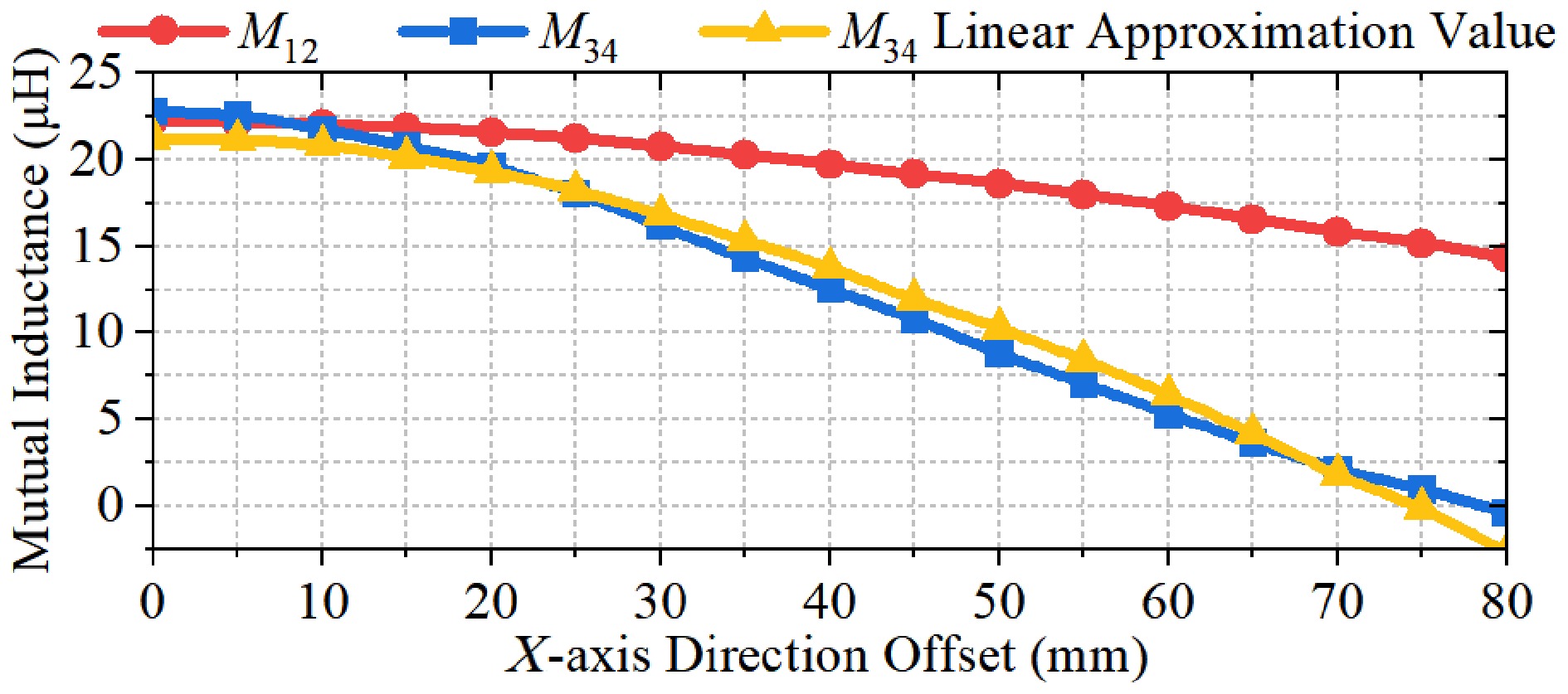
Figure 8.
The linear approximation value, and the actual value of the M34 line.
The maximum offset in the X-axis direction of this paper is set at 80 mm. Then, at the maximum offset point, the main mutual inductances have their minimum value, which are M12min = 14.35 μH, and M34min = −0.39 μH, respectively. Firstly, assuming that the F(M12) determined by Eq. (14) is monotonically decreasing: through Eq. (18), the range of L2 is calculated to be L2 ≥ 90.38 μH and L2 ≤ 70.46 μH, and there is no intersection, thus L2 does not exist in this case; through Eq. (20), the range of L2 is calculated to be L2 ≤ 51.00 μH and L2 ≥ 59.90 μH, and there is also no intersection, thus L2 does not exist in this case either.
Let's consider the case where F(M12) exhibits non-monotonic variation: According to Eq. (21), the range of L2 obtained through calculation is [51.00, 90.38] μH; according to Eq. (23), the range of L2 is [63.30, 137.44] μH; and according to Eq. (25), the range of L2 is L2 ≤ 72.03 μH. Therefore, when the minimum value of M12 is taken at the position shown in Fig. 7c, these ranges yield the range of L2 as [63.30, 72.03] μH.
Due to the certain deviation between the linear approximation value of M34, and the actual value, in the range of [63.30, 72.03] μH, L2 and the corresponding L1 may cause an overvoltage phenomenon in practical applications. Therefore, it is necessary to verify L2 within this range, and if necessary, optimize the values within a small range outside the interval to avoid overvoltage. Substitute the actual measured main mutual inductance M12 and M34 into the voltage gain GVV expression shown in Eq. (6), and the optimized design curves of GVV when different L2 are substituted can be obtained, as shown in Fig. 9.
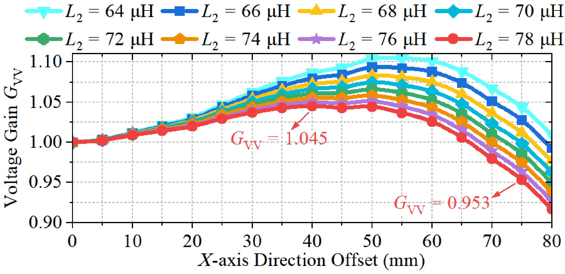
Figure 9.
Voltage gain GVV under different L2 values.
It can be observed that within the range of [63.30, 72.03] μH for determining the value of L2, by substituting L2 with 64, 66, 68, 70, and 72 μH, respectively, resulting in an overvoltage phenomenon. If L2 is further increased beyond this range, by substituting L2 with 74, 76, and 78 μH, respectively, the maximum value of GVV will continue to gradually decrease. When L2 = 78 μH, the maximum value of GVV decreases to within 1.05, eliminating the overvoltage phenomenon. However, at the 80 mm offset point in the X-axis direction, GVV < 0.95, while at the 75 mm offset point, GVV > 0.95 can still be achieved. Thus, approximately 5 mm of the maximum offset range is sacrificed. Considering the safety and maximum offset range of the system, this paper selects L2 to be 78 μH. The actual measured value of the inductor after precise winding is 78.64 μH, and substituting it into Eq. (11) yields L1 = 15.77 μH. The actual measured value of L1 after precise winding is also approximately 15.77 μH. Substituting the obtained value of L1 and L2 into Eqs. (3) and (4), the values of all compensation capacitors C1, C2, C3, C4, CP, and CS can be calculated.
Installation of a magnetic shielding device
-
In this paper, COMSOL finite element simulation software is used to simulate the magnetic flux density distribution. Figure 10 shows the magnetic flux density distribution of the proposed self-decoupling cross coil at its rated operating position, where Fig. 10a is the side view of the XOZ plane, and Fig. 10b is the side view of the YOZ plane. The exposure limit of the general public under the guidance of ICNIRP is 27 μT, and the Tx is excited by the current 1 A. The exposure limit of 27 μT is marked with a dashed white line. It can be found that the magnetic flux density distribution of the self-decoupling cross coil is relatively uniform, and Rx has a certain inhibition effect on the magnetic flux density above it, but there is still a small amount of magnetic leakage.
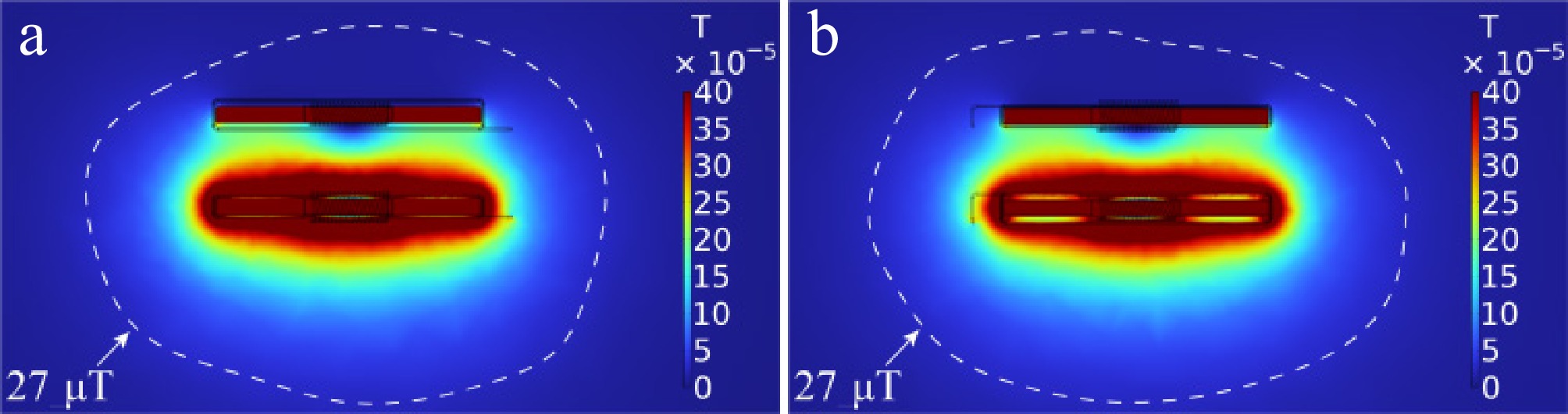
Figure 10.
The magnetic flux density distribution of the self-decoupled cross coil presented. (a) Side view of the XOZ plane. (b) Side view of the YOZ plane.
A 1-mm-thick plate measuring 300 mm in both length and width was installed 10 mm above the receiving magnetic coupler (Rx). This plate functions as a magnetic shield, effectively containing stray magnetic fields and ensuring operator safety. As can be seen from Fig. 11, the intense magnetic-field region between Tx and Rx remains essentially unchanged, while magnetic leakage above the shield is greatly reduced to under 27 μT.
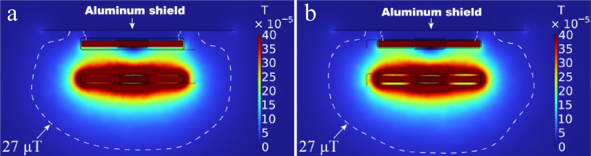
Figure 11.
Magnetic flux density distribution of the proposed self-decoupling cross coil after magnetic shielding. (a) Side view of the XOZ plane. (b) Side view of the YOZ plane.
Furthermore, in practical applications, the receiving end of this magnetic coupling mechanism can be installed at the bottom of the AGV, and the metal body itself can achieve effective magnetic shielding.
-
A 200 W output power experimental platform was built to test and verify the effectiveness of the proposed hybrid-topology WPT system, as illustrated in Fig. 12.
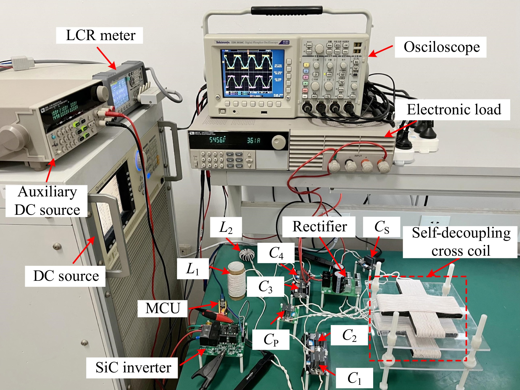
Figure 12.
Photograph of the experimental platform.
Key parameters of the WPT system
-
Table 1 presents the key parameters of the hybrid topology WPT system, with all inductance and capacitance values being actual measured data.
Table 1. Key parameters of the experimental prototype.
Parameters Value Parameters Value LP1 111.61 μH L1 15.77 μH LP2 110.63 μH L2 78.64 μH LS1 115.38 μH CP 31.73 nF LS2 112.01 μH CS 30.39 nF C1 222.48 nF C3 18.37 nF C2 27.52 nF C4 44.57 nF M12N 22.21 μH M34N 22.79 μH M12min 14.35 μH M34min −0.39 μH a 3.043 b −46.34 μH f0 85 kHz GVVN 1 hN 45 mm Uin 60 V Δ 5% RLN 15 Ω In Fig. 13, the size of the proposed self-decoupling cross coil is 159 mm × 159 mm × 10 mm. The material of the ferrite is PC95. All the coils and inductors are wound using Leeds wire with a specification of 300 × 0.12 mm.
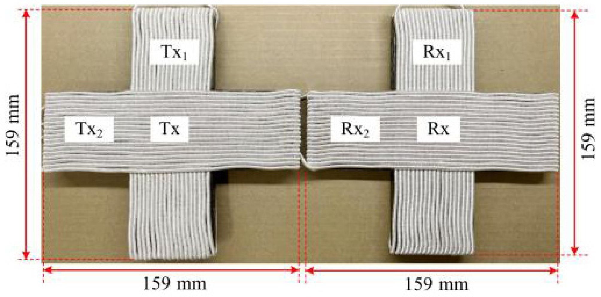
Figure 13.
Photo of decoupled cross coil.
Experimental results when the X-axis direction has offset
-
The output voltage and efficiency when the X-axis direction has an offset are shown in Fig. 14. It can be observed that when the X-axis direction offset is 50 mm, the maximum output voltage fluctuation δV = 4.99% < 5%. When the threshold condition of δV ≤ 5% is met, the maximum offset in the X-axis direction can reach 85 mm, and at this time, the output voltage fluctuation δV = 4.93%, and the maximum offset range is 53.46% (85 mm/159 mm). Compared with the voltage gain GVV optimization design curve shown in Fig. 9, the actual maximum offset range of the system can reach 85 mm, which is slightly better than the 75 mm calculated in Fig. 9. From the rated working position to the maximum offset position, the DC-DC efficiency η of the system generally shows a downward trend with small fluctuations, and the efficiency range is 86.41%−89.06%.
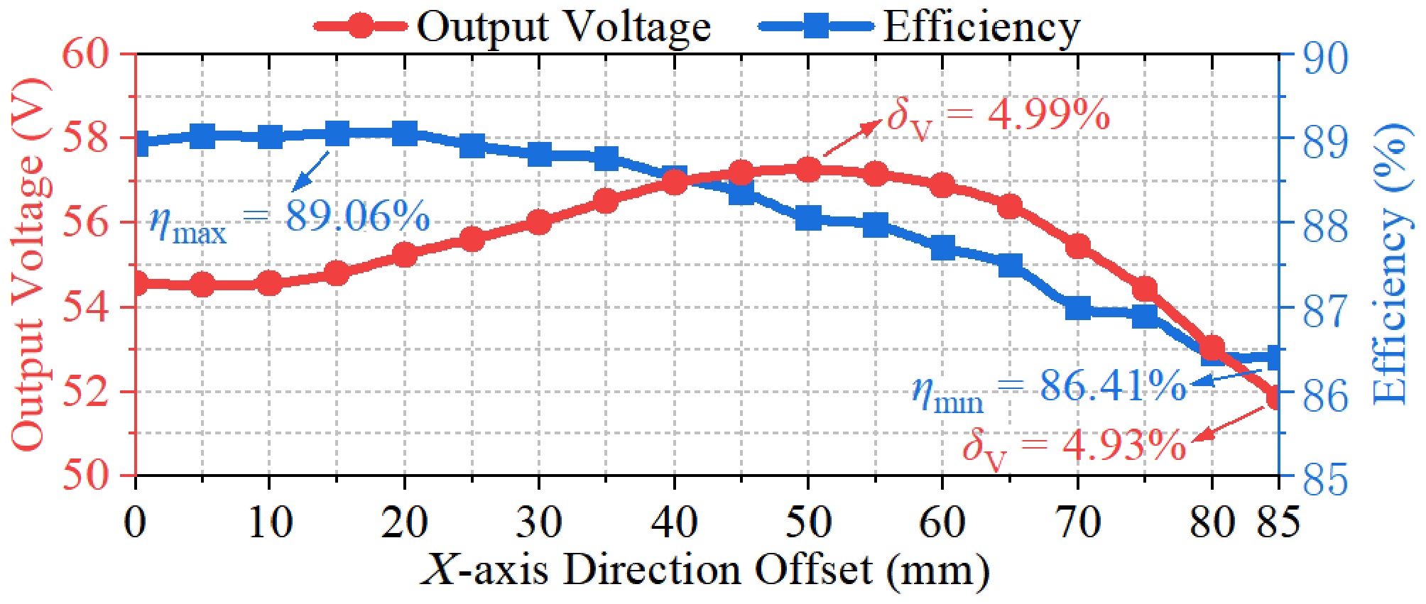
Figure 14.
Output voltage and efficiency when the X-axis direction is offset.
When the X-axis offset varies, the experimental waveforms of Up, Ip, uE and iE are shown in Fig. 15. The experimental waveforms from the rated working position to the maximum offset X = 85 mm remain almost unchanged, which verifies the strong anti-offset performance of the proposed hybrid topological WPT system in the X-axis direction. And, as indicated by the red circle, Ip always lags behind Up by a small phase angle, achieving a zero voltage switch (ZVS) at the transmitting end. This also indicates that the system can realize zero phase angle (ZPA), verifying the conclusion derived from Eq. (7).
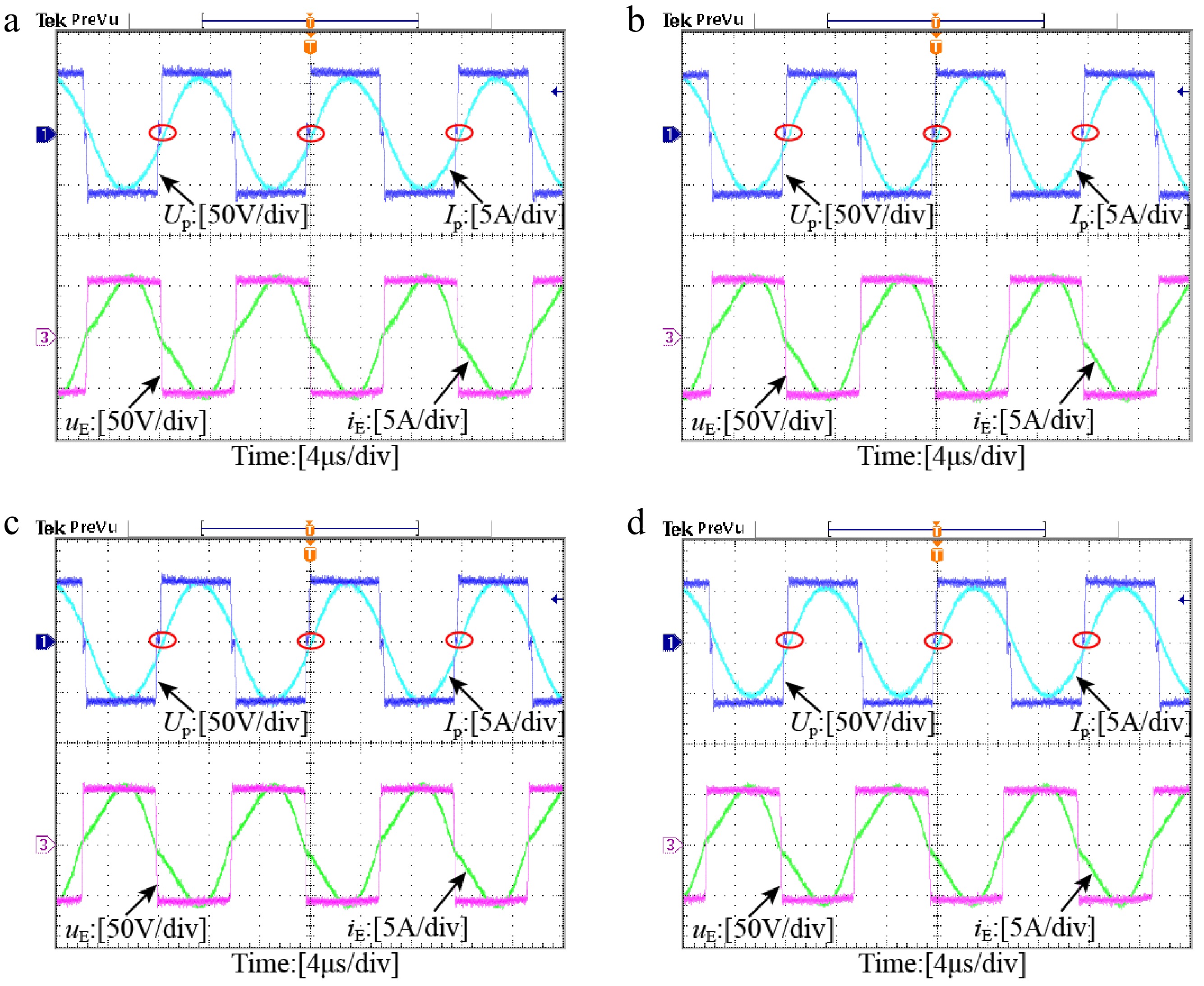
Figure 15.
Experimental waveforms under different X-axis offsets. (a) X = 0. (b) X = 30 mm. (c) X = 60 mm. (d) X = 85 mm.
Experimental results when the Y-axis direction has offset
-
The output voltage and efficiency when the Y-axis direction has an offset are shown in Fig. 16. When the threshold condition δV ≤ 5% is met, the maximum offset in the Y-axis direction can reach 15 mm, at which point the output voltage fluctuation δV = 4.88%, and the maximum offset range is 9.43% (15 mm/159 mm), which is much smaller than that when the X-axis direction has an offset. This is mainly because the trend of the main mutual inductances change in the Y-axis direction is opposite to that in the X-axis direction. As shown in the mutual inductances measurement results in Figs. 4b and 5b, the quantitative relationship between the main mutual inductances M12 and M34 has reversed at this time, while the compensation inductances L1 and L2 in the circuit have not correspondingly reversed their values, resulting in the system being unable to maintain the same output voltage characteristics as the X-axis direction offset when there is a large Y-axis direction offset. However, within the offset range of 0 to 10 mm, regardless of whether it is an X-axis direction offset or a Y-axis direction offset, M12 and M34 are approximately equal, so the output voltage characteristics of the Y-axis direction offset can be maintained the same as those of the X-axis direction offset. Starting from the 15 mm offset position, when the Y-axis direction is offset, M12 is significantly smaller than M34, and the system output voltage begins to drop significantly. Below a 15 mm offset distance, it is difficult to control the voltage drop within 5% range. Considering that AGVs usually have sensor guidance when moving along the X-axis direction, their Y-axis direction offset is relatively small. Therefore, the anti-offset performance of the system proposed in this paper in the Y-axis direction is acceptable. From the rated working position to the maximum offset position, the fluctuation range of the system's DC-DC efficiency is 88.92% to 89.13%. When offsetting to 45 mm, it can still maintain 83.57%.
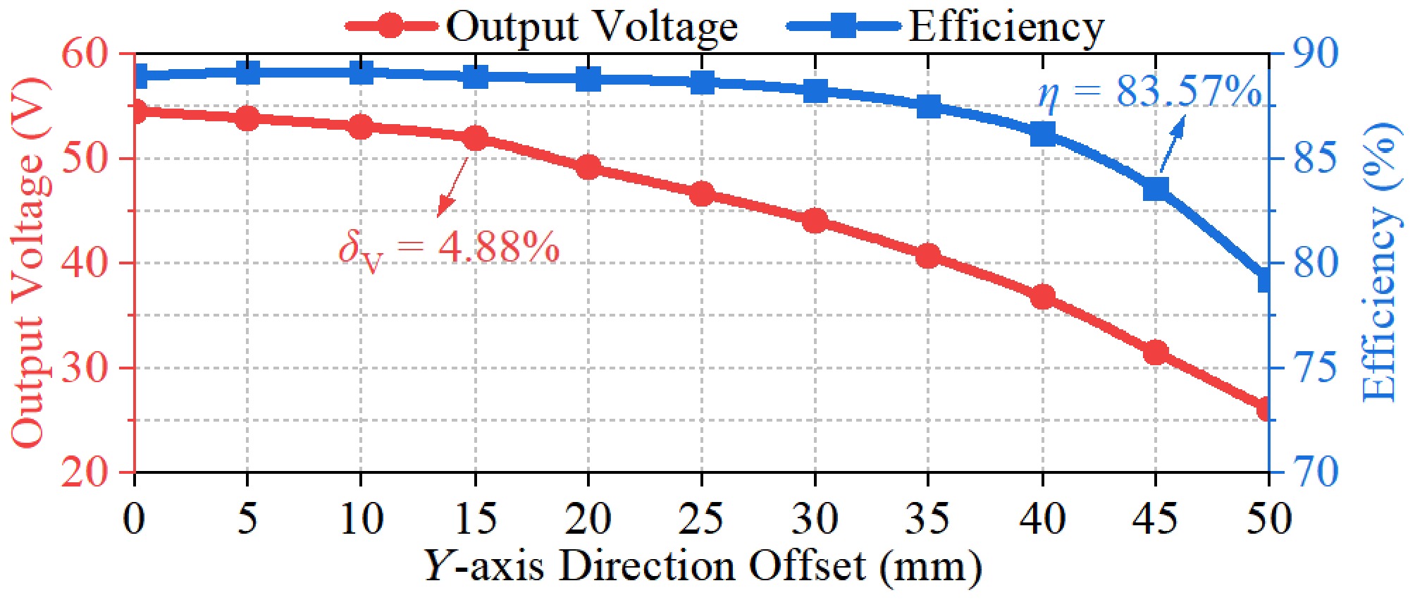
Figure 16.
Output voltage and efficiency when the Y-axis direction is offset.
When the Y-axis direction is shifted differently, the experimental waveforms of Up, Ip, uE, and iE are shown in Fig.17. Within the maximum offset range, the experimental waveforms are almost the same as those at the rated working position, and Ip still lags behind Up by a very small phase angle, achieving ZVS at the transmitting end. This also indicates that the system can realize ZPA, verifying that the proposed system has certain anti-offset performance in the Y-axis direction.
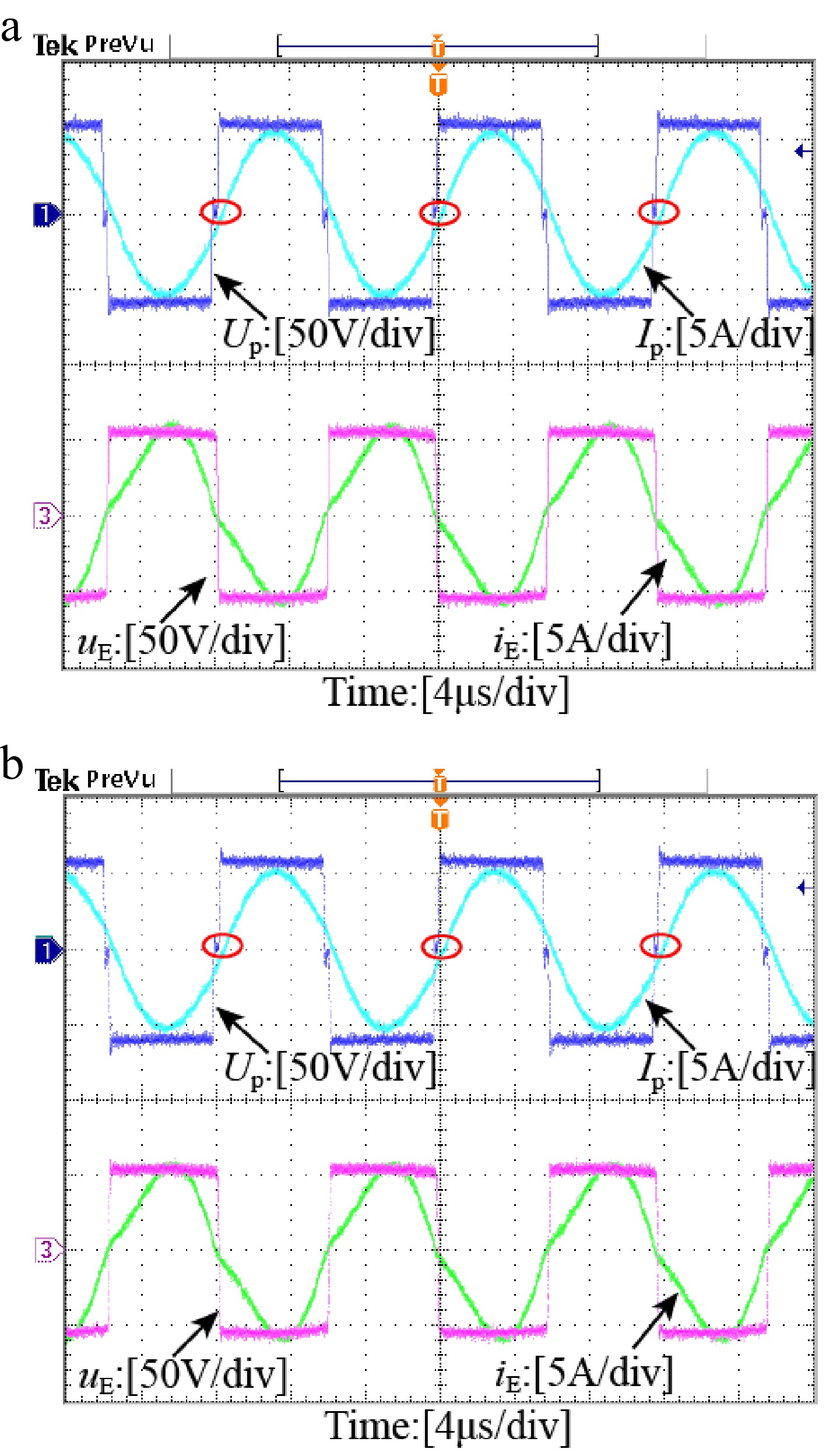
Figure 17.
Experimental waveforms under different Y-axis offset conditions. (a) Y = 10 mm. (b) Y = 15 mm.
Experimental results under different transmission distances (Z-axis offset)
-
The output voltages and efficiencies under different transmission distances h (Z-axis direction offset) are shown in Fig. 18. When the threshold condition δV ≤ 5% is met, the transmission distance h can range from 28 to 51 mm, corresponding to a Z-axis direction offset of −17 to +6 mm, respectively. Thus, the maximum offset range is −37.78% to +13.33% (−17 mm/45 mm to +6 mm/45 mm), and the system DC-DC efficiencies at the maximum offset are 86.81% and 88.56%, respectively.
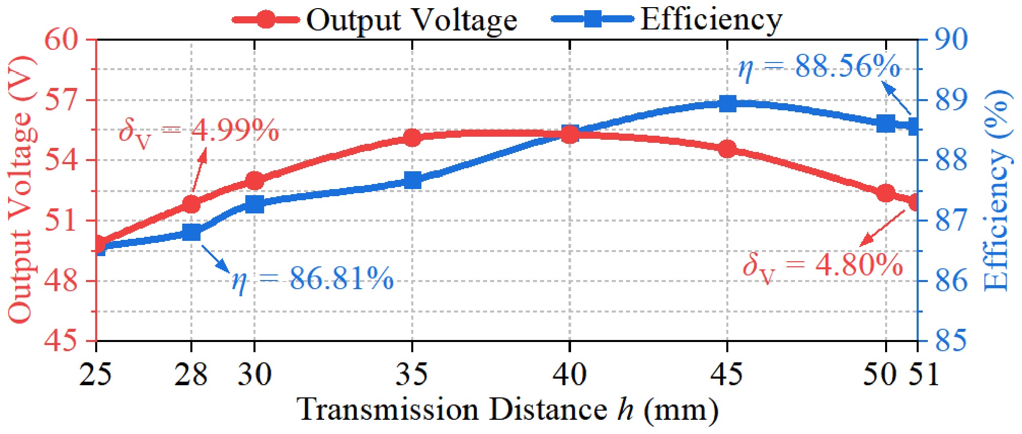
Figure 18.
Output voltage and efficiency when the Z-axis direction is offset.
When the Z-axis offset varies, the experimental waveforms of Up, Ip, uE, and iE are shown in Fig. 19. When the transmission distance h = 28 mm, the waveforms of uE and iE still remain basically unchanged, but the phase angle of Ip lagging behind Up has significantly increased, resulting in more reactive power being introduced into the system. This will cause the system resonance to be disrupted. Therefore, when the transmission distance is reduced, the efficiency decreases significantly. When the transmission distance h = 56 mm, the experimental waveforms are almost the same as the rated working position, and Ip still lags behind Up by a very small phase angle. The system can achieve ZPA. Therefore, the proposed system can also maintain a certain output voltage even when the transmission distance h is significantly reduced.
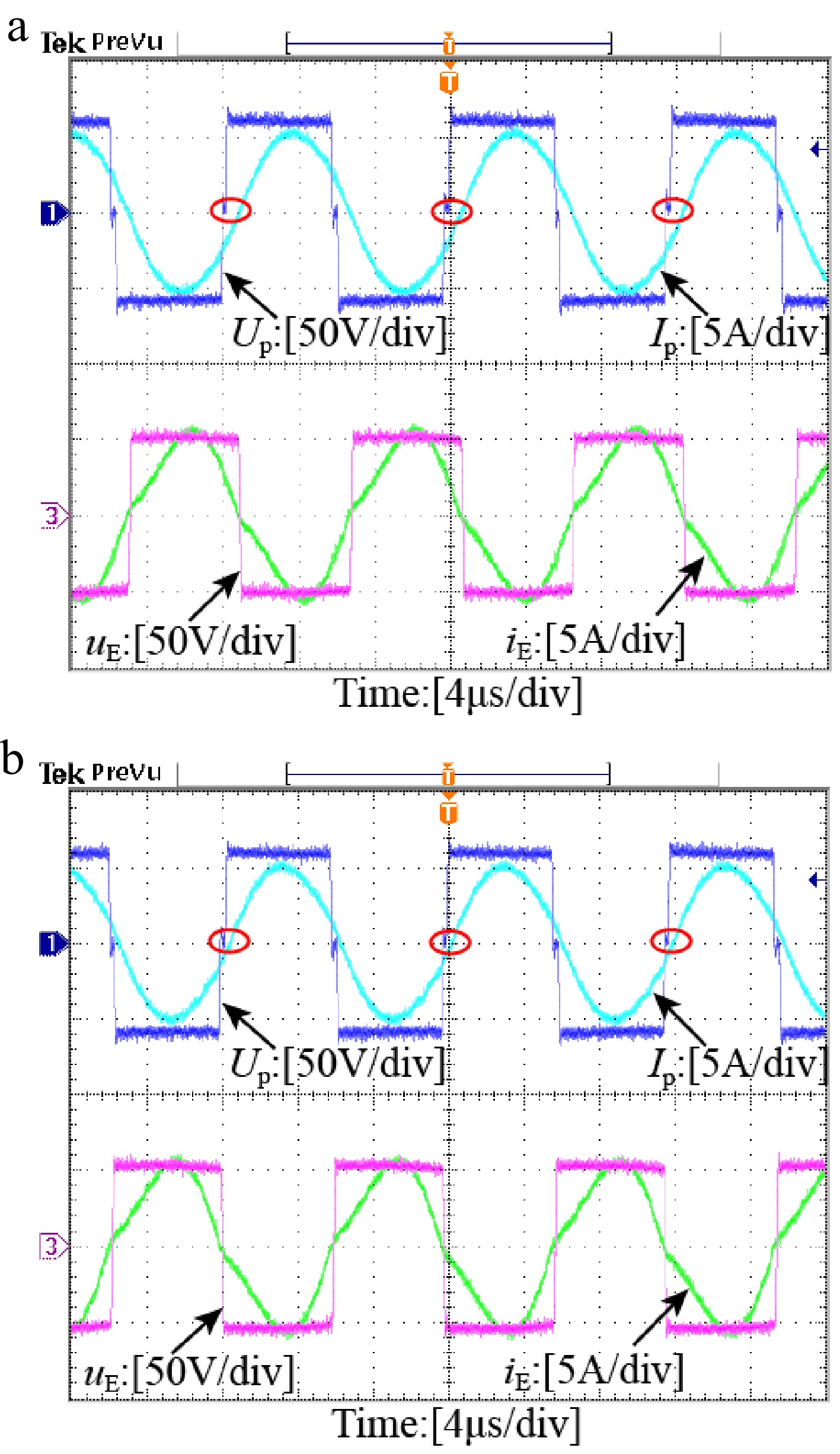
Figure 19.
Experimental waveforms under different Z-axis offsets. (a) h = 28 mm. (b) h = 51 mm.
Experimental results under different load resistances RL
-
The output voltage and efficiency under different load resistances are shown in Fig. 20. When the threshold condition δV ≤ 5% is met, the load resistance RL can reach 45 Ω at light load, which is 300% of the rated load resistance RLN. At this time, the output voltage fluctuation δV = 4.28%, and the system DC-DC efficiency is 86.17%. For heavy load, if the load resistance RL is 10 Ω, the output voltage fluctuation δV = 3.27% < 5%, still meeting the design requirements, and the system DC-DC efficiency is 86.90%. It can be seen that the proposed hybrid topological WPT system can achieve constant voltage (CV) output characteristics independent of the load, verifying the conclusion derived from Eq. (6). It can also be noted that the output voltage is larger when the load is lighter, and it will significantly decrease when the load is heavier. When the load resistance RL = 20 Ω, the maximum system DC-DC efficiency is 89.00%.
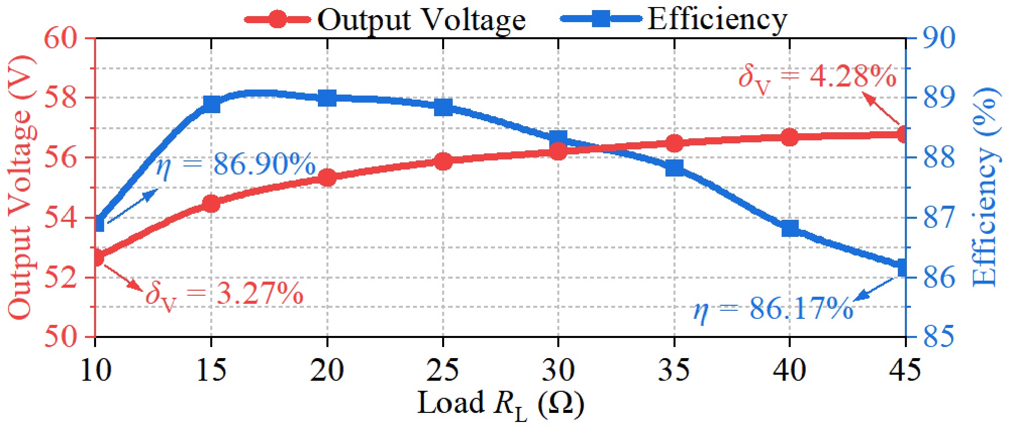
Figure 20.
Output voltage and efficiency under different load resistances RL.
When the load resistance RL is 45 Ω, the experimental waveforms of Up, Ip, uE, and iE at the rated working position and the maximum offset are shown in Fig. 21, respectively. The output voltage is slightly increased compared with the rated load resistance RLN = 15 Ω, but still meets the threshold condition of δV ≤ 5%, verifying the load independence of the system. The output waveforms at the rated working position and the maximum offset remain basically unchanged, verifying that the system also has strong anti-offset performance in the X-axis direction when the rated load resistance is 300%. Moreover, as the offset along the X-axis increases, the phase angle lagging behind Up by Ip becomes significantly larger. This leads to the system introducing more reactive power, resulting in a decrease in efficiency.
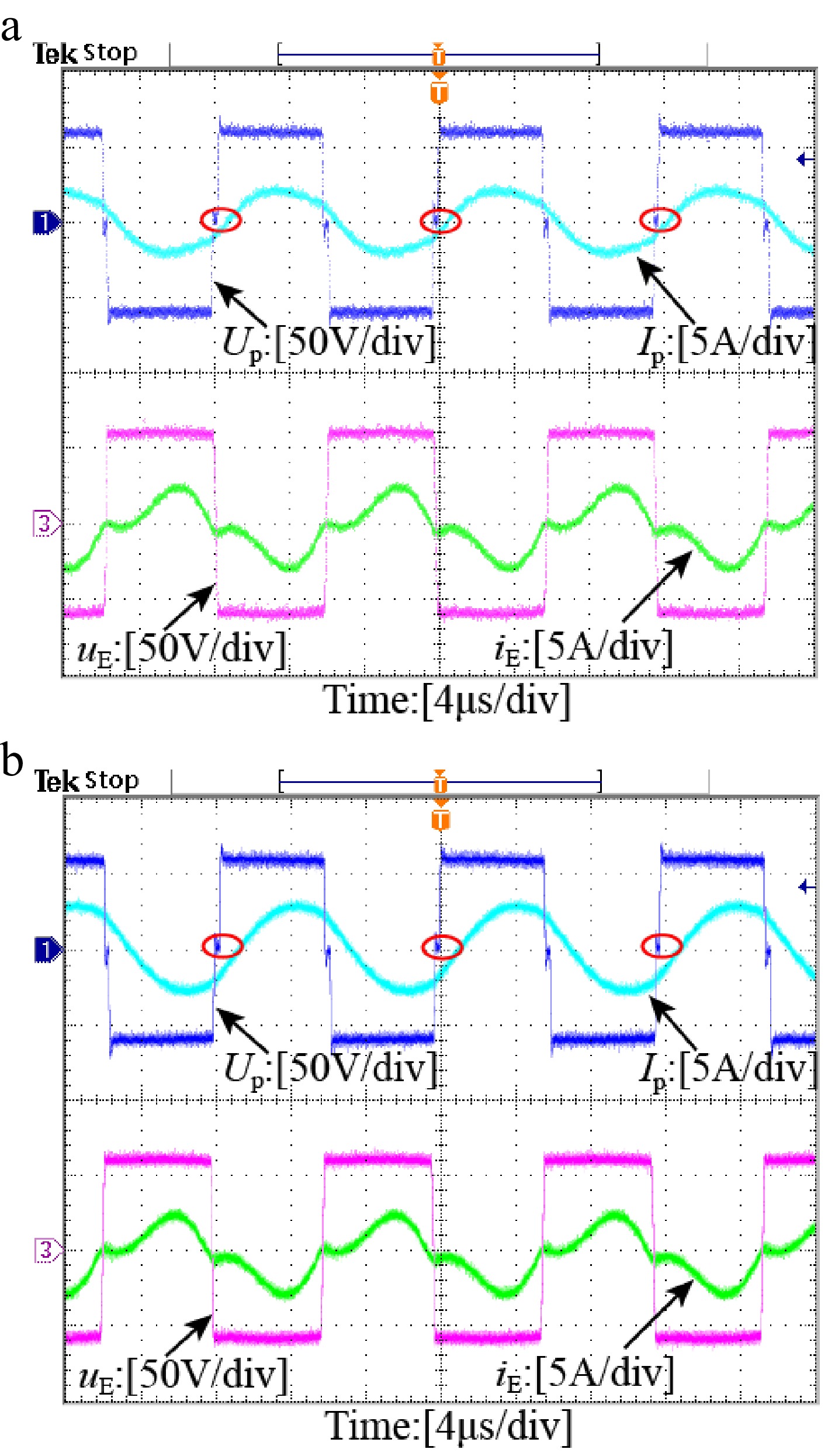
Figure 21.
Experimental waveforms under different X-axis offsets when the load resistance is 45 Ω. (a) X = 0. (b) X = 30 mm.
Experimental results in a weak coupling
-
When Rx is placed away from Tx, the system is in a weak coupling state, where M12 and M34 are approximately equal to zero. At this time, the experimental waveforms of Up, Ip, uE, and i1 are shown in Fig. 22. It can be observed that uE is almost equal to zero, indicating that the output voltage of the system is very small at this time. In the weak coupling state, zero-voltage output can be achieved, verifying the conclusion in Eq. (5) that M12 ≈ M34 ≈ 0 and IE is close to zero. At the same time, the value of Ip is also very small, verifying the conclusion in Eq. (5) that Ip is close to zero. At this time, the current i1 in the Rx1 coil is not zero, and its phase is approximately 90° different from Up, verifying the expression of I1 in Eq. (5).
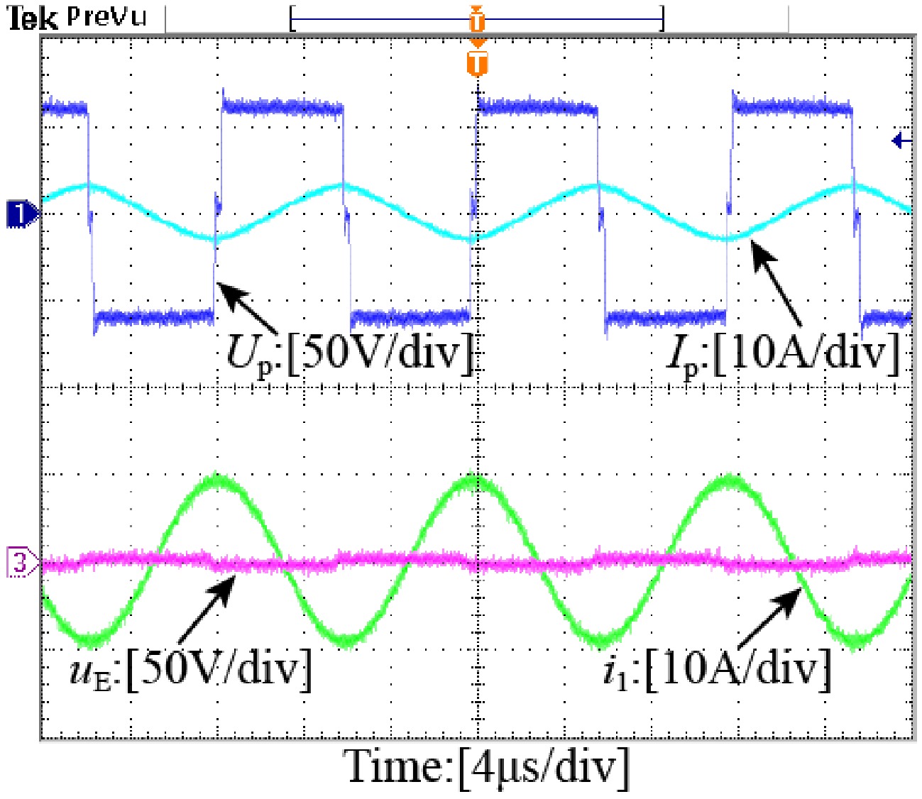
Figure 22.
Experimental waveforms showing that the system is in a weak coupling state when Rx is far away from Tx.
Dynamic experimental waveforms
-
Figure 23 shows the experimental waveforms of the dynamic output voltage and current. As can be seen from Fig. 23a, when the receiving coil suddenly shifts in the X-axis direction (changing from X = 0 to X = 40 mm), both the output current and voltage will decrease. The adjustment time is approximately 120 μs. The voltage still meets the threshold condition of δV ≤ 5%, which is in line with the conclusion from the experimental results when the X-axis direction has offset. As can be seen from Fig. 23b, when the load resistance changes (from RL = 15 Ω to RL = 45 Ω), the output current decreases, but the output voltage increases. The overshoot of the output voltage is 4.8%, and the adjustment time is approximately 100 μs. Under steady-state conditions, the output voltage still meets the threshold condition of δV ≤ 5%, which is consistent with the conclusion drawn from the experimental results under different load resistances RL.
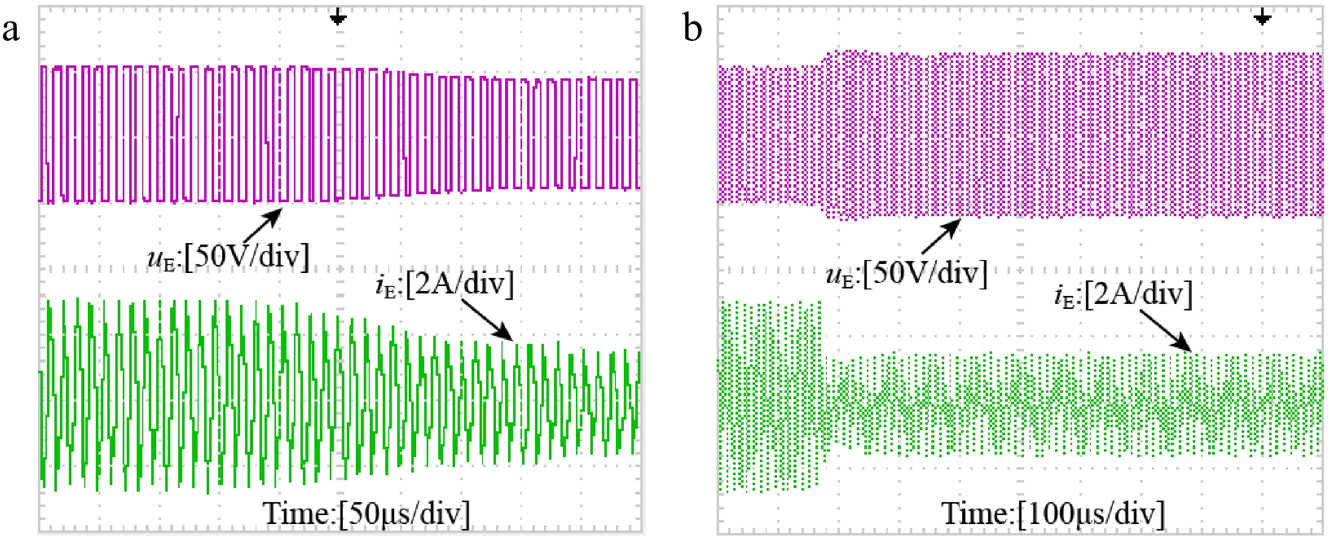
Figure 23.
Dynamic experimental waveforms. (a) The X-axis offset value changes from X = 0 to X = 40 mm. (b) The load resistance changes from RL = 15 Ω to RL = 45 Ω.
Power analysis
-
When h = hN = 45 mm, the power loss distribution at X = 0 and Y = 0 is shown in Fig. 24. All the data were measured by the power analyzer (GPM 8330). Clearly, the loss of the magnetic coupling mechanism accounts for the majority of the system loss (69.3%), while the losses of the inverter (20%) and the rectifier (10.7%) are also significant. The losses of inverters and rectifiers can be improved by choosing more suitable semiconductor components. The loss of the magnetic coupling mechanism is very high. This is likely due to the large number of coils and the high internal resistance. Increasing the system power can effectively reduce the loss in this part.
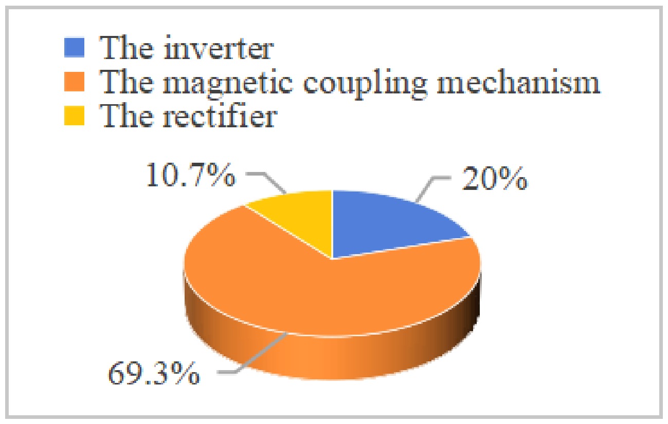
Figure 24.
Power loss distribution.
Summary and comparison
-
In conclusion, under the weak coupling condition of the system, zero-voltage output can be realized. Notably, i1—the current flowing through Rx1 (the only coil with a relatively large current magnitude)—is confined within a reasonable range. This eliminates the risks of overvoltage and overcurrent, thus guaranteeing the system's operational safety. For an extra layer of safety during weak coupling, this paper recommends shutting down the inverter when there is no AGV undergoing wireless charging. This measure helps reduce the magnetic field induced by the current in Rx1, thereby minimizing potential hazards to the surrounding environment and on-site personnel.
To further illustrate the superiority of the proposed hybrid topology WPT system, in Table 2, the proposed hybrid topology is compared with the related studies of existing hybrid topologies. The definitions of X and Y directions follow the original text. From the comparison, it can be found that the proposed hybrid topology in this paper can achieve a 53.5% offset range in the X direction. This data outperforms other systems that are also dedicated to improving the anti-offset capability in a single direction[18,19]. Compared to systems that aim to enhance the anti-offset capability in both vertical directions of a plane[24,25], it can significantly improve the anti-offset capability in a single direction. The total offset range of the Z-axis accounted for 51.1%, and was also superior in all the studies. Additionally, thanks to the large negative offset range of the Z-axis (−37.8%), the AGV can still obtain a stable output voltage, even when the vehicle body sinks due to heavy loads.
Table 2. Comparison with existing research on hybrid topology.
Ref. Topology structure h (cm) Coil structure Wire coil size (cm) Offset range (cm) Output fluctuation Load independent Weak coupling security [17] S-S LCC-LCC 12 BP X: 39.1
Y: 73.8X: 16 (40.9%)
Y: No data
Z: −2~+2
(−16.7%~+16.7%)5% CC NO [18] S-S LCC-LCC 12 DD X: 77.5
Y: 39.1X: 12 (15.5%)
Y: 16 (40.9%)
Z: −2~+2
(−16.7%~+16.7%)5% CC YES [24] S-S LCC-LCC 7.5 Unipolar coil and novel
bipolar coil combinationX: 30
Y: 30X: 7.5 (25%)
Y: 7.5 (25%)
Z: No Data7% CC YES LCC-S S-LCC 1% CV [25] LCC-S S-LCC 7 Crossed solenoid magnetic coupler X: 22
Y: 22X: 9 (40.9%)
Y: 9 (40.9%)
Z: 0~40 (0~57.1%)5% CV YES This paper CLC-S S-CLC 4.5 Self-decoupled
cross-windingX: 15.9
Y: 15.9X: 8.5 (53.5%)
Y: 1.5 (9.4%)
Z: −1.7~+0.6
(−37.8%~+13.3%)5% CV YES h represents the transmission distance. -
This paper presents a novel hybrid topology wireless power transfer (WPT) system specifically designed for automatic guided vehicles (AGVs). By analyzing the parameter design process of the hybrid topology WPT system, the parameter setting and compensation component optimization for any displacement range have been simplified. Experiments fully verified the strong anti-offset performance of the system in the X-axis direction, while the offset range in the Y-axis direction was relatively small but met the compatibility requirements of conventional AGV systems. Under different transmission distances h, the maximum offset range was −37.78% to +13.33%, which met the demand for tire compression under the condition of a large AGV load. Additionally, under different load conditions, the system always met the threshold condition, and the efficiency remained above 86%. The experimental results fully demonstrated that the systematically designed WPT system is more suitable for the demands of actual production.
Further development should prioritize the structural and material optimization of ferrite components, with clear targets set for weight saving and cost reduction, thereby increasing the overall cost-effectiveness of the hybrid topology-based wireless charging system. The weak anti-offset performance of the Y-axis can also be avoided by means such as stop slots, thus preventing the reduction in charging efficiency. To achieve stringent misalignment tolerance in both the X and Y axes, the parameter design must be further optimized. Specifically, the inductance L2 must be constrained according to the profiles in Figs. 4 and 5, to enable it to mitigate the concurrent voltage fluctuations resulting from reductions in both M12 and M34. The 200 W WPT system is suitable for the actual operation of some small AGVs. The specific working mode of the AGV can be quantitatively matched with the 200 W charging capacity to make the most appropriate decision. Additionally, the 200 W wireless charging system is an ideal and practical starting point. By accumulating experience in the control interface, electromagnetic compatibility, and thermal management of the 200 W system, it will be a smooth transition if a larger power system needs to be developed in the future.
-
The authors confirm their contributions to the paper as follows: study conception and design: Lu W, Chen M, Zhang C; data collection: Chen M, Zhang C; analysis, review, and results verification of algorithms and simulation results: Chen M, Zhang C, Chen H; manuscript correction, analysis correction, and editing: Lu W, Chen M, Zhang C, Xu D. All authors reviewed the results and approved the final version of the manuscript.
-
The datasets generated during and/or analyzed in the current study are available from the corresponding author on reasonable request.
-
This research was funded by the National Natural Science Foundation of China (Grant Nos 51407084, 62222307), the China Postdoctoral Science Foundation (Grant No. 2017M610294), and the Jiangsu Planned Projects for Postdoctoral Research Funds (Grant No. 1701092B).
-
The authors declare that they have no conflict of interest.
- Copyright: © 2026 by the author(s). Published by Maximum Academic Press, Fayetteville, GA. This article is an open access article distributed under Creative Commons Attribution License (CC BY 4.0), visit https://creativecommons.org/licenses/by/4.0/.
-
About this article
Cite this article
Lu W, Chen M, Zhang C, Chen H, Xu D. 2026. A hybrid topology wireless charging system for AGVs with strong anti-offset performance. Wireless Power Transfer 13: e014 doi: 10.48130/wpt-0026-0005 

A hybrid topology wireless charging system for AGVs with strong anti-offset performance
- Received: 10 October 2025
- Revised: 11 December 2025
- Accepted: 07 January 2026
- Published online: 30 May 2026
Abstract: When AGVs are parked for wireless charging, misalignment and offset between the transmitting and receiving coils are prone to occur, which affects the charging power and efficiency. To address this issue, this paper proposes a novel flat cross-shaped self-decoupling electromagnetic coupler for AGVs that require strong anti-offset performance in a hybrid topology wireless charging system. Firstly, a hybrid topology combining CLC-S compensation topology and S-CLC compensation topology is proposed. The principle of achieving anti-offset, the load-independent output characteristics, and the safety of the system in a weak coupling state are analyzed. Secondly, a new magnetic coupling mechanism is proposed, which can eliminate all cross-couplings generated in the proposed hybrid topology. Finally, a 200 W output power experimental platform is built. The maximum DC-DC efficiency of the system is 89.13%. The maximum X-axis offset of the system reaches 53.46% of the coil size, the maximum Y-axis offset is 9.43% of the coil size, and the maximum Z-axis offset reaches −37.78% to +13.33% of the rated transmission distance. The load-independent constant voltage output characteristics of the proposed system and its safety in a weak coupling state are also verified.